

Page 1
5
4
3
2
1
D D
Topstar Digital technologies Co.,LTD
01. Title
Board name: MotherBoard Schematic
Project name: F42
Version: VerC
Initial Date:
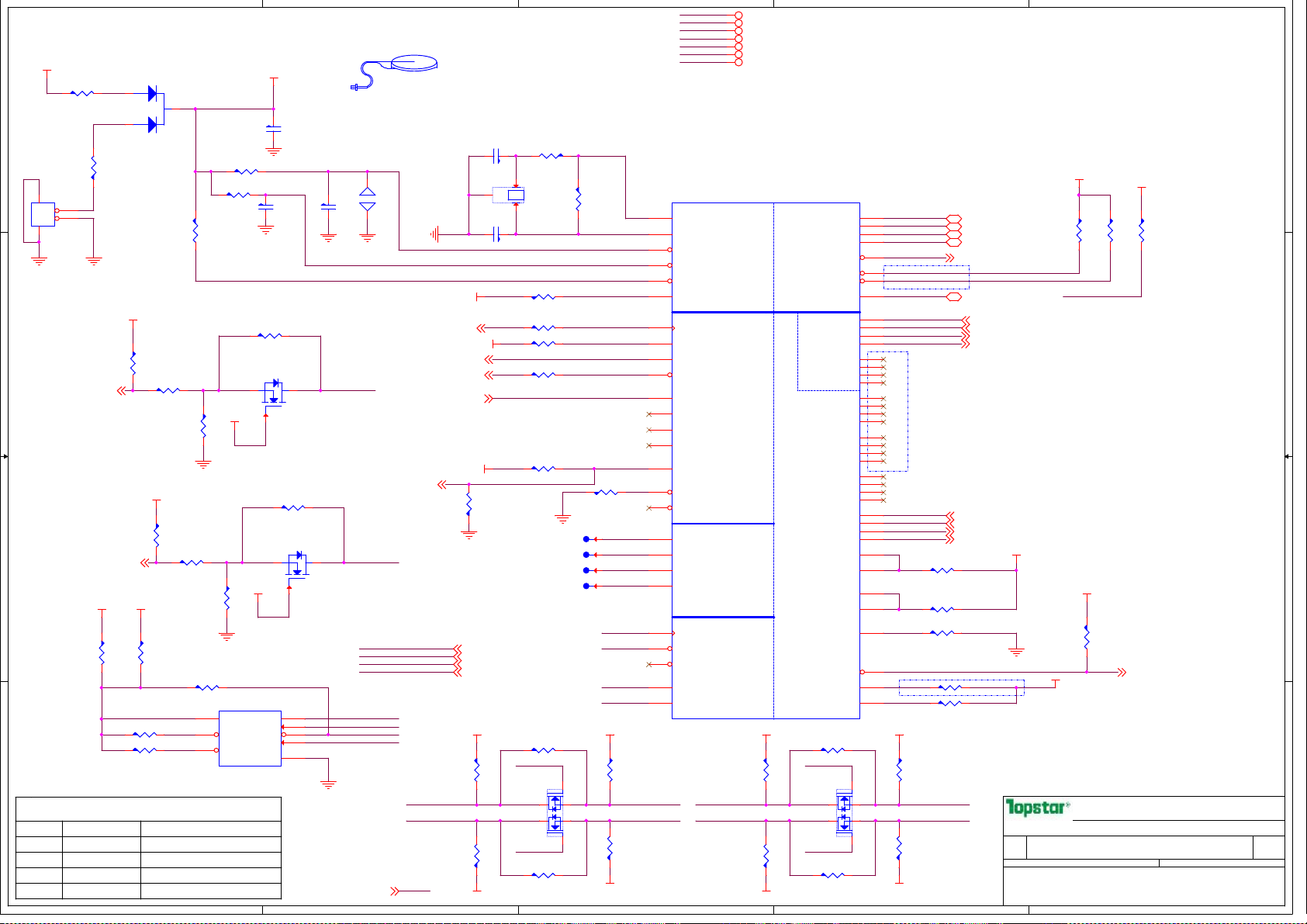
02. Sys block
03. PWR block
04. Notes
05. Modify and history
06. Ivy Bridge DMI/FDI/PCIE
07.Ivy Bridge CLK/MISC
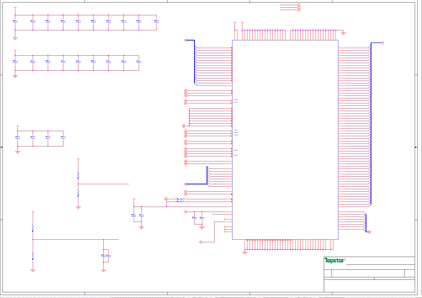
08. Ivy Bridge DDR3
09. Ivy Bridge Vcore/VTT
10. Ivy Bridge VGFX/VDDQ
C C
11. Ivy Bridge GND
12. Ivy Bridge Reserved
13. DDR3 CHA SODIMM0
14. DDR3 CHB SODIMM0
Topstar Confidential
Hardware drawing by: Hardware check by: EMI Check by:
15. PCH RTC/SATA/SPI/HDA/LPC
16. PCH PCIE/CLK/SMBUS
17. PCH DMI/FDI/PWRGD
18. PCH Display
19. PCH PCI/USB
20. PCH GPIO
21. PCH PWR 1/2
22. PCH PWR 2/2
23. PCH GND
24. LVDS&Inverter CONN
25. HDMI CONN
26. CRT Interface
27. SATA HDD&ODD
28. TP Module&BD CONN
B B
Power drawing by:
Power check by:
Manager Sign by:
A A
Page Name
Page Name
Page Name
Size
Size
Size
Project Name Rev
Project Name Rev
Project Name Rev
A3
A3
A3
Date: Sheet of
Date: Sheet of
Date: Sheet of
PROPERTY NOTE: this document contains information confidential and property to
PROPERTY NOTE: this document contains information confidential and property to
PROPERTY NOTE: this document contains information confidential and property to
TOPSTAR and shall not be reproduced or transferred to other documents or disclosed
TOPSTAR and shall not be reproduced or transferred to other documents or disclosed
TOPSTAR and shall not be reproduced or transferred to other documents or disclosed
to others or used for any purpose other than that for which it was obtained without
to others or used for any purpose other than that for which it was obtained without
to others or used for any purpose other than that for which it was obtained without
the expressed written consent of TOPSTAR
the expressed written consent of TOPSTAR
the expressed written consent of TOPSTAR
5
4
3
2
TOPSTAR TECHNOLOGY
TOPSTAR TECHNOLOGY
TOPSTAR TECHNOLOGY
杨华明
(Sky Yang)
杨华明
(Sky Yang)
杨华明
(Sky Yang)
Title(Cover Page)
Title(Cover Page)
Title(Cover Page)
CL42 EVT
CL42 EVT
CL42 EVT
1
A
A
1 51Sunday, April 07, 2013
1 51Sunday, April 07, 2013
1 51Sunday, April 07, 2013
A
Page 2
5
4
3
2
1
Topstar Confidential
ShenZhen Topstar Industry Co.,LTD
D D
CL341 SYSTEM BLOCK Ver:C
CHA DDR3 SODIMM0
IVY Bridage
Backlight
Connector
+VDC
LED Panel
+V3.3S
C C
LVDS
BIOS
32Mbit
+V3.3S
SPI
BGA1023
+VCC_CORE,+VccGFX
+V1.5, +V1.8S,
+V1.05S
+VCCSA
FDI
GEN 2 DMI*4
Panther Point
989 FCBGA
+V3.3A,+V3.3S,+V1.5S,
+V1.05S,+V1.8S,
PCIE mini Card
HDMI
+V5S
PCIE 1X
+V5A,+V5S
LPC
USB1.1/2.0
DDR3 1333/1600
DDR3 1333/1600
PECI3.0
PCIE 1X
RTL8105E/RTL8111E
USB2.0
AZALIA
SATA ODD
NA
CHB DDR3 SODIMM1
1333/1600
+V0.75S,+V1.5,+V3.3S
+V0.75S,+V1.5,+V3.3S
RJ45
+V3.3S,+V3.3AL
+V5S
S-ATA
2.5" HDD
+V5S,+V3.3S
Card Reader
RTS5138-GR
+V3.3S,+V3.3AL
RJ45
SD/MMC/MS CARD
USB PORT0/1
B B
+V5AL
BLUE
TOOTH(V2.1)
BCM-2046/CCOM
+V3.3AL
+V3.3S
Camera
1.3M/2.0M
MODULE
KB Controller/EC
ENE 3930
+V3.3AL,+V3.3S
PECI3.0
L
R
AZALIA
ALC269
+V5S,+V3.3S
LED/TouchPAD/Button/
A A
5
4
KB Matrix
LID
DAUGHTER BOARD
3
2
MiC
TOPSTAR TECHNOLOGY
TOPSTAR TECHNOLOGY
TOPSTAR TECHNOLOGY
杨华明
(Sky Yang)
杨华明
(Sky Yang)
杨华明
Page Name
Page Name
Page Name
Size
Size
Size
Project Name Rev
Project Name Rev
Project Name Rev
A3
A3
A3
Date: Sheet of
Date: Sheet of
Date: Sheet of
PROPERTY NOTE: this document contains information confidential and property to
PROPERTY NOTE: this document contains information confidential and property to
PROPERTY NOTE: this document contains information confidential and property to
TOPSTAR and shall not be reproduced or transferred to other documents or disclosed
TOPSTAR and shall not be reproduced or transferred to other documents or disclosed
TOPSTAR and shall not be reproduced or transferred to other documents or disclosed
to others or used for any purpose other than that for which it was obtained without
to others or used for any purpose other than that for which it was obtained without
to others or used for any purpose other than that for which it was obtained without
the expressed written consent of TOPSTAR
the expressed written consent of TOPSTAR
the expressed written consent of TOPSTAR
Sys block
Sys block
Sys block
CL42 EVT
CL42 EVT
CL42 EVT
(Sky Yang)
1
2 51Sunday, April 07, 2013
2 51Sunday, April 07, 2013
2 51Sunday, April 07, 2013
A
A
A
Page 3

5
D D
C C
4
3
2
1
B B
A A
Page Name
Page Name
Page Name
Size
Size
Size
Project Name Rev
Project Name Rev
Project Name Rev
A3
A3
A3
Date: Sheet of
Date: Sheet of
Date: Sheet of
PROPERTY NOTE: this document contains information confidential and property to
PROPERTY NOTE: this document contains information confidential and property to
PROPERTY NOTE: this document contains information confidential and property to
TOPSTAR and shall not be reproduced or transferred to other documents or disclosed
TOPSTAR and shall not be reproduced or transferred to other documents or disclosed
TOPSTAR and shall not be reproduced or transferred to other documents or disclosed
to others or used for any purpose other than that for which it was obtained without
to others or used for any purpose other than that for which it was obtained without
to others or used for any purpose other than that for which it was obtained without
the expressed written consent of TOPSTAR
the expressed written consent of TOPSTAR
the expressed written consent of TOPSTAR
5
4
3
2
TOPSTAR TECHNOLOGY
TOPSTAR TECHNOLOGY
TOPSTAR TECHNOLOGY
杨华明
(Sky Yang)
杨华明
(Sky Yang)
杨华明
(Sky Yang)
PWR Block
PWR Block
PWR Block
CL42 EVT
CL42 EVT
CL42 EVT
1
A
A
3 51Wednesday, January 09, 2013
3 51Wednesday, January 09, 2013
3 51Wednesday, January 09, 2013
A
Page 4
5
D D
C C
4
3
2
1
B B
A A
Page Name
Page Name
Page Name
Size
Size
Size
Project Name Rev
Project Name Rev
Project Name Rev
A3
A3
A3
Date: Sheet of
Date: Sheet of
Date: Sheet of
PROPERTY NOTE: this document contains information confidential and property to
PROPERTY NOTE: this document contains information confidential and property to
PROPERTY NOTE: this document contains information confidential and property to
TOPSTAR and shall not be reproduced or transferred to other documents or disclosed
TOPSTAR and shall not be reproduced or transferred to other documents or disclosed
TOPSTAR and shall not be reproduced or transferred to other documents or disclosed
to others or used for any purpose other than that for which it was obtained without
to others or used for any purpose other than that for which it was obtained without
to others or used for any purpose other than that for which it was obtained without
the expressed written consent of TOPSTAR
the expressed written consent of TOPSTAR
the expressed written consent of TOPSTAR
5
4
3
2
TOPSTAR TECHNOLOGY
TOPSTAR TECHNOLOGY
TOPSTAR TECHNOLOGY
杨华明
(Sky Yang)
杨华明
(Sky Yang)
杨华明
(Sky Yang)
Notes
Notes
Notes
CL42 EVT
CL42 EVT
CL42 EVT
1
A
A
4 51Wednesday, January 09, 2013
4 51Wednesday, January 09, 2013
4 51Wednesday, January 09, 2013
A
Page 5

5
4
3
2
1
2012-5-16 VerA First Release.
D D
C C
B B
A A
Page Name
Page Name
Page Name
Size
Size
Size
Project Name Rev
Project Name Rev
Project Name Rev
A3
A3
A3
Date: Sheet of
Date: Sheet of
Date: Sheet of
PROPERTY NOTE: this document contains information confidential and property to
PROPERTY NOTE: this document contains information confidential and property to
PROPERTY NOTE: this document contains information confidential and property to
TOPSTAR and shall not be reproduced or transferred to other documents or disclosed
TOPSTAR and shall not be reproduced or transferred to other documents or disclosed
TOPSTAR and shall not be reproduced or transferred to other documents or disclosed
to others or used for any purpose other than that for which it was obtained without
to others or used for any purpose other than that for which it was obtained without
to others or used for any purpose other than that for which it was obtained without
the expressed written consent of TOPSTAR
the expressed written consent of TOPSTAR
the expressed written consent of TOPSTAR
5
4
3
2
TOPSTAR TECHNOLOGY
TOPSTAR TECHNOLOGY
TOPSTAR TECHNOLOGY
杨华明
(Sky Yang)
杨华明
(Sky Yang)
杨华明
(Sky Yang)
Modify and history
Modify and history
Modify and history
CL42 EVT
CL42 EVT
CL42 EVT
1
A
A
5 51Wednesday, January 09, 2013
5 51Wednesday, January 09, 2013
5 51Wednesday, January 09, 2013
A
Page 6
5
U16A
DMI_TXN017
DMI_TXN117
DMI_TXN217
FDI_TXN[7:0]17
FDI_TXP[7:0]17
FDI_FSYNC017
FDI_FSYNC117
FDI_LSYNC017
FDI_LSYNC117
+V1.05S
DMI_TXN317
DMI_TXP017
DMI_TXP117
DMI_TXP217
DMI_TXP317
DMI_RXN017
DMI_RXN117
DMI_RXN217
DMI_RXN317
DMI_RXP017
DMI_RXP117
DMI_RXP217
DMI_RXP317
FDI_INT17
R206
24.9,1%
R0402
5
D D
C C
B B
Layout notice:
A A
DMI_TXN0
DMI_TXN1
DMI_TXN2
DMI_TXN3
DMI_TXP0
DMI_TXP1
DMI_TXP2
DMI_TXP3
DMI_RXN0
DMI_RXN1
DMI_RXN2
DMI_RXN3
DMI_RXP0
DMI_RXP1
DMI_RXP2
DMI_RXP3
FDI_TXN0
FDI_TXN1
FDI_TXN2
FDI_TXN3
FDI_TXN4
FDI_TXN5
FDI_TXN6
FDI_TXN7
FDI_TXP0
FDI_TXP1
FDI_TXP2
FDI_TXP3
FDI_TXP4
FDI_TXP5
FDI_TXP6
FDI_TXP7
DP_COMP
M2
P6
P1
P10
N3
P7
P3
P11
K1
M8
N4
R2
K3
M7
P4
T3
U7
W11
W1
AA6
W6
V4
Y2
AC9
U6
W10
W3
AA7
W7
T4
AA3
AC8
AA11
AC12
U11
AA10
AG8
AF3
AD2
AG11
AG4
AF4
AC3
AC4
AE11
AE7
AC1
AA4
AE10
AE6
IC,IVB_2CBGA,0P7
BGA1023_31X24
4
DMI_RX#[0]
DMI_RX#[1]
DMI_RX#[2]
DMI_RX#[3]
DMI_RX[0]
DMI_RX[1]
DMI_RX[2]
DMI_RX[3]
DMI_TX#[0]
DMI_TX#[1]
DMI_TX#[2]
DMI_TX#[3]
DMI_TX[0]
DMI_TX[1]
DMI_TX[2]
DMI_TX[3]
FDI0_TX#[0]
FDI0_TX#[1]
FDI0_TX#[2]
FDI0_TX#[3]
FDI1_TX#[0]
FDI1_TX#[1]
FDI1_TX#[2]
FDI1_TX#[3]
FDI0_TX[0]
FDI0_TX[1]
FDI0_TX[2]
FDI0_TX[3]
FDI1_TX[0]
FDI1_TX[1]
FDI1_TX[2]
FDI1_TX[3]
FDI0_FSYNC
FDI1_FSYNC
FDI_INT
FDI0_LSYNC
FDI1_LSYNC
eDP_COMPIO
eDP_ICOMPO
eDP_HPD#
eDP_AUX#
eDP_AUX
eDP_TX#[0]
eDP_TX#[1]
eDP_TX#[2]
eDP_TX#[3]
eDP_TX[0]
eDP_TX[1]
eDP_TX[2]
eDP_TX[3]
4
PEG_ICOMPI
PEG_ICOMPO
PEG_RCOMPO
PEG_RX#[0]
PEG_RX#[1]
DMI Intel(R) FDI
eDP
PEG_RX#[2]
PEG_RX#[3]
PEG_RX#[4]
PEG_RX#[5]
PEG_RX#[6]
PEG_RX#[7]
PEG_RX#[8]
PEG_RX#[9]
PEG_RX#[10]
PEG_RX#[11]
PEG_RX#[12]
PEG_RX#[13]
PEG_RX#[14]
PEG_RX#[15]
PEG_RX[0]
PEG_RX[1]
PEG_RX[2]
PEG_RX[3]
PEG_RX[4]
PEG_RX[5]
PEG_RX[6]
PEG_RX[7]
PEG_RX[8]
PEG_RX[9]
PEG_RX[10]
PEG_RX[11]
PEG_RX[12]
PEG_RX[13]
PEG_RX[14]
PEG_RX[15]
PEG_TX#[0]
PEG_TX#[1]
PEG_TX#[2]
PEG_TX#[3]
PEG_TX#[4]
PEG_TX#[5]
PEG_TX#[6]
PEG_TX#[7]
PEG_TX#[8]
PEG_TX#[9]
PEG_TX#[10]
PEG_TX#[11]
PEG_TX#[12]
PEG_TX#[13]
PEG_TX#[14]
PCI EXPRESS -- GRAPHICS
PEG_TX#[15]
PEG_TX[0]
PEG_TX[1]
PEG_TX[2]
PEG_TX[3]
PEG_TX[4]
PEG_TX[5]
PEG_TX[6]
PEG_TX[7]
PEG_TX[8]
PEG_TX[9]
PEG_TX[10]
PEG_TX[11]
PEG_TX[12]
PEG_TX[13]
PEG_TX[14]
PEG_TX[15]
3
G3
PEG_IRCOMP_R
G1
G4
H22
J21
B22
D21
A19
D17
B14
D13
A11
B10
G8
A8
B6
H8
E5
K7
K22
K19
C21
D19
C19
D16
C13
D12
C11
C9
F8
C8
C5
H6
F6
K6
G22
C23
D23
F21
H19
C17
K15
F17
F14
A15
J14
H13
M10
F10
D9
J4
F22
A23
D24
E21
G19
B18
K17
G17
E14
C15
K13
G13
K10
G10
D8
K4
3
R195 24.9,1%
R0402
Layout notice:
+V1.05S
2
+V1.05S 7,9,15,16,17,21,22,30,41,44,47
TOPSTAR TECHNOLOGY
TOPSTAR TECHNOLOGY
TOPSTAR TECHNOLOGY
Robin
Robin
Robin
Page Name
Page Name
Page Name
Size
Size
Size
Project Name Rev
Project Name Rev
Project Name Rev
A4
A4
A4
Date: Sheet of
Date: Sheet of
Date: Sheet of
PROPERTY NOTE: this document contains information confidential and property to
PROPERTY NOTE: this document contains information confidential and property to
PROPERTY NOTE: this document contains information confidential and property to
TOPSTAR and shall not be reproduced or transferred to other documents or disclosed
TOPSTAR and shall not be reproduced or transferred to other documents or disclosed
TOPSTAR and shall not be reproduced or transferred to other documents or disclosed
to others or used for any purpose other than that for which it was obtained without
to others or used for any purpose other than that for which it was obtained without
to others or used for any purpose other than that for which it was obtained without
the expressed written consent of TOPSTAR
the expressed written consent of TOPSTAR
the expressed written consent of TOPSTAR
2
Ivy Bridge DMI/FDI/PCIE
Ivy Bridge DMI/FDI/PCIE
Ivy Bridge DMI/FDI/PCIE
CL42 EVT
CL42 EVT
CL42 EVT
1
A
A
A
6 51Wednesday, January 09, 2013
6 51Wednesday, January 09, 2013
6 51Wednesday, January 09, 2013
1
Page 7
5
4
差异
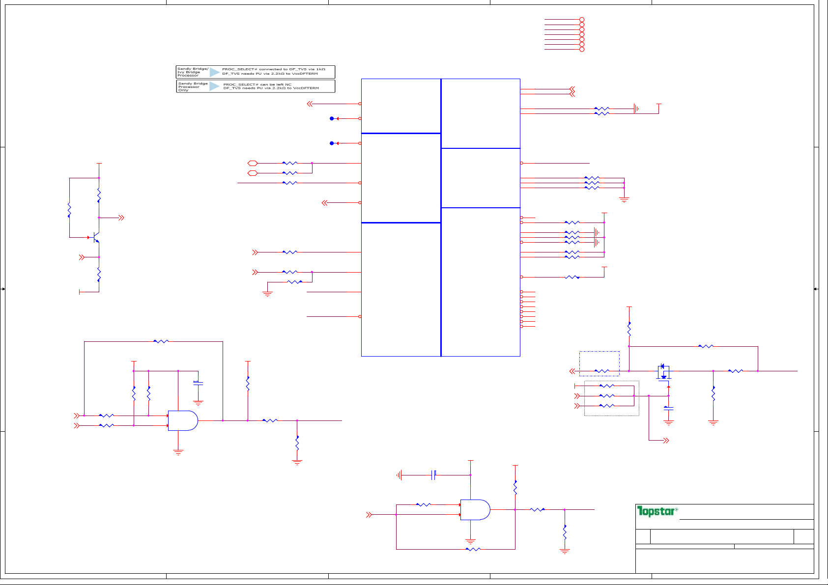
1:Processor type
Sandy Bridge: Output High;
Ivy Bridge: Output low
3
2
+V3.3S 14,15,16,17,18,19,20,21,22,24,25,29,30,31,32,33,34,35,40,41,42,43,44,45,47
+V1.05S 6,9,15,16,17,21,22,30,41,44,47
+V1.5 14,40,45
+V3.3SB 15,17,20,22,28,31,33,35,37,38,39,45
+V3.3AL 15,16,17,19,20,22,24,28,31,33,40,43,45
+V1.5S_CPU_VDDQ
+V1.5S 10,21,31,45
1
BUF_PLT_RST#19,31,33,34
U16B
F49
PRO C_SELE CT#
C57
PRO C_DETE CT#
ICTP
C49
CAT ERR#
A48
ICTP
PEC I
C45
PRO CHOT#
D45
THER MTRIP#
C48
PM_SYNC
B46
UNCORE PWRG OOD
BE4 5
SM_DR AMPWR OK
D44
RES ET#
IC,IVB_2CBGA,0P7
BGA1023_31X24
MISC THERMAL PWR MANAGEMENT
CLOCKS
DDR3
JTAG & BPM
TU142 VerB: Changed R297 to 1k and ns R720 for DRAMRST#
isolate circuit control in Deep S3 2011-12-20
+V3.3AL
C0402
C177 0.1uF/10V,X7R
ns
R710 0
3
R0402
1
2
R363 0
DPL L_REF_ CLK
DPL L_REF_ CLK#
SM_DR AMRST#
SM_RC OMP[0]
SM_RC OMP[1]
SM_RC OMP[2]
MISC
U2
53
VCC
GND
SN74AHC1G08DBV
SOT23_5
R0402ns
4
BCL K
BCL K#
PRD Y#
PRE Q#
TCK
TMS
TRS T#
TDO
DBR #
BPM#[0 ]
BPM#[1 ]
BPM#[2 ]
BPM#[3 ]
BPM#[4 ]
BPM#[5 ]
BPM#[6 ]
BPM#[7 ]
+V1.05S
J3
H2
AG3
CLK_DP_P_R
AG1
CLK_DP_N_R
AT3 0
BF4 4
SM_RCOMP_0
BE4 3
SM_RCOMP_1
BG4 3
SM_RCOMP_2
N53
N55
PREQ#
L56
TCK
L55
TMS
J58
TRST#
M60
TDI
TDI
L59
TDO
K58
DBR#
G58
E55
E59
G55
G59
H60
J59
J61
DDR3_DRAMRST#14
DRAMRST_CNTRL_PCH16
EC_DRAMRST_CNTRL_PCH33
R246
75
R0402
ns
CPU_DRAMRST#
R185 51nsR0402
R190 51 R0402ns
R191 51 R0402ns
R193 51 R0402ns
R189 51 R0402ns
R194 51 R0402ns
R146 1K R0402
+V3.3AL
PLT_RST#_R
R247
2.2K
R0402
CLK_EXP_P 16
CLK_EXP_N 16
R492 1K R0402
R496 1K R0402
R244 140ohm 1%R0402
R243 25.5ohm 1%R0402
R236 200,1% R0402
+V1.05S
+V3.3S
Place near to DIMM
R267
1K
R0402
R720 1K R0402
R278 0 R0402
R297 1K
R0402
R238
1.05K 1%
R0402
2
+V1.05S
+V1.5
R268
1K
R0402
R265 0
Q13
L2N7002LT1G
SOT23
3
2
ns
Page Name
Page Name
Page Name
Size
Size
Size
PROPERTY NOTE: this document contains information confidential and property to
PROPERTY NOTE: this document contains information confidential and property to
PROPERTY NOTE: this document contains information confidential and property to
TOPSTAR and shall not be reproduced or transferred to other documents or disclosed
TOPSTAR and shall not be reproduced or transferred to other documents or disclosed
TOPSTAR and shall not be reproduced or transferred to other documents or disclosed
to others or used for any purpose other than that for which it was obtained without
to others or used for any purpose other than that for which it was obtained without
to others or used for any purpose other than that for which it was obtained without
the expressed written consent of TOPSTAR
the expressed written consent of TOPSTAR
the expressed written consent of TOPSTAR
1
C173
470pF/25V,X7R
C0402
DRAMRST_CNTRL 10
Project Name Rev
Project Name Rev
Project Name Rev
A3
A3
A3
Date: Sheet of
Date: Sheet of
Date: Sheet of
ns
R0402
R264 0
R262
4.99K,1%
R0402
TOPSTAR TECHNOLOGY
TOPSTAR TECHNOLOGY
TOPSTAR TECHNOLOGY
Robin
Robin
Robin
Ivy Bridge CLK/MISC
Ivy Bridge CLK/MISC
Ivy Bridge CLK/MISC
CL42 EVT
CL42 EVT
CL42 EVT
1
R0402
CPU_DRAMRST#
7 51Wednesday, January 09, 2013
7 51Wednesday, January 09, 2013
7 51Wednesday, January 09, 2013
A
A
A
D D
H_SNB_IVB#20
T17
ns
T69
ns
+V1.05S
R241
75
1
2 3
R531 0 R0402
R534 0 R0402
5
R0402
VR_PROCHOT# 44
Q11
LMBT3904LT1G
SOT23
R266
10K
R0402
R530
10K
R0402
ns
+V3.3AL
R695 0
R528
200,1%
R0402
1
2
R0402
ns
U20
53
VCC
GND
SN74AHC1G08DBV
SOT23_5
R248
1K
C C
EC_PROCHOT#33
B B
PM_DRAM_PWRGD17
MAIN_PWROK17,33,43
Note:
When implement S3 power save function, need to mount
S3_Power_Save option
A A
R0402
+V3.3SB
H_PM_SYNC17
H_CPUPWRGD20
C363
0.1uF/10V,X7R
C0402
4
H_PECI20
H_PECI_EC33
VR_PROCHOT#
+V1.5S
4
R696
200,1%
R0402
ns
R539 2.37K,1%
R0402
R154 0
R155 47
R147 56
R156 0
R171 0
H_PECI_R
ns
R0402
DG要求R147为43 ohm 5%
R0402
R0402
THERMTRIP#20,30
H_PM_SYNC_R
R0402
H_CPUPWRGD_R
R0402
10KR172
R0402
SM_DRAMPWROK
PLT_RST#_R
Note: Not mount R696 when S3 power save
Note:
S3 power save option: R539:2.37K, R234:2K
No S3 power save option: R539:0ohm, R234:ns
SM_DRAMPWROK
R234
2K,1%
R0402
Page 8
5
4
3
2
1
U16C
AG6
SA_ DQ[0]
D D
C C
B B
AJ6
AP1 1
AL6
AJ1 0
AJ8
AL8
AL7
AR1 1
AP6
AU6
AV9
AR6
AP8
AT1 3
AU13
BC7
BB7
BA1 3
BB1 1
BA7
BA9
BB9
AY13
AV1 4
AR1 4
AY17
AR1 9
BA1 4
AU14
BB1 4
BB1 7
BA4 5
AR4 3
AW 48
BC4 8
BC4 5
AR4 5
AT4 8
AY48
BA4 9
AV4 9
BB5 1
AY53
BB4 9
AU49
BA5 3
BB5 5
BA5 5
AV5 6
AP5 0
AP5 3
AV5 4
AT5 4
AP5 6
AP5 2
AN57
AN53
AG5 6
AG5 3
AN55
AN52
AG5 5
AK5 6
BD3 7
BF3 6
BA2 8
BE3 9
BD3 9
AT4 1
SA_ DQ[1]
SA_ DQ[2]
SA_ DQ[3]
SA_ DQ[4]
SA_ DQ[5]
SA_ DQ[6]
SA_ DQ[7]
SA_ DQ[8]
SA_ DQ[9]
SA_ DQ[10]
SA_ DQ[11]
SA_ DQ[12]
SA_ DQ[13]
SA_ DQ[14]
SA_ DQ[15]
SA_ DQ[16]
SA_ DQ[17]
SA_ DQ[18]
SA_ DQ[19]
SA_ DQ[20]
SA_ DQ[21]
SA_ DQ[22]
SA_ DQ[23]
SA_ DQ[24]
SA_ DQ[25]
SA_ DQ[26]
SA_ DQ[27]
SA_ DQ[28]
SA_ DQ[29]
SA_ DQ[30]
SA_ DQ[31]
SA_ DQ[32]
SA_ DQ[33]
SA_ DQ[34]
SA_ DQ[35]
SA_ DQ[36]
SA_ DQ[37]
SA_ DQ[38]
SA_ DQ[39]
SA_ DQ[40]
SA_ DQ[41]
SA_ DQ[42]
SA_ DQ[43]
SA_ DQ[44]
SA_ DQ[45]
SA_ DQ[46]
SA_ DQ[47]
SA_ DQ[48]
SA_ DQ[49]
SA_ DQ[50]
SA_ DQ[51]
SA_ DQ[52]
SA_ DQ[53]
SA_ DQ[54]
SA_ DQ[55]
SA_ DQ[56]
SA_ DQ[57]
SA_ DQ[58]
SA_ DQ[59]
SA_ DQ[60]
SA_ DQ[61]
SA_ DQ[62]
SA_ DQ[63]
SA_ BS[0]
SA_ BS[1]
SA_ BS[2]
SA_ CAS#
SA_ RAS#
SA_ WE#
SA_ DQS#[0]
SA_ DQS#[1]
SA_ DQS#[2]
SA_ DQS#[3]
SA_ DQS#[4]
SA_ DQS#[5]
SA_ DQS#[6]
SA_ DQS#[7]
DDR SYSTEM MEMORY A
SA_ CK[0]
SA_ CK#[0]
SA_ CKE[0]
SA_ CK[1]
SA_ CK#[1]
SA_ CKE[1]
SA_ CS#[0]
SA_ CS#[1]
SA_ ODT[0]
SA_ ODT[1]
SA_ DQS[0]
SA_ DQS[1]
SA_ DQS[2]
SA_ DQS[3]
SA_ DQS[4]
SA_ DQS[5]
SA_ DQS[6]
SA_ DQS[7]
SA_ MA[0]
SA_ MA[1]
SA_ MA[2]
SA_ MA[3]
SA_ MA[4]
SA_ MA[5]
SA_ MA[6]
SA_ MA[7]
SA_ MA[8]
SA_ MA[9]
SA_ MA[10]
SA_ MA[11]
SA_ MA[12]
SA_ MA[13]
SA_ MA[14]
SA_ MA[15]
AU36
AV3 6
AY26
AT4 0
AU40
BB2 6
BB4 0
BC4 1
AY40
BA4 1
AL1 1
AR8
AV1 1
AT1 7
AV4 5
AY51
AT5 5
AK5 5
AJ1 1
AR1 0
AY11
AU17
AW 45
AV5 1
AT5 6
AK5 4
BG3 5
BB3 4
BE3 5
BD3 5
AT3 4
AU34
BB3 2
AT3 2
AY32
AV3 2
BE3 7
BA3 0
BC3 0
AW 41
AY28
AU26
MB_DATA[63:0]14
MB_B_BS014
MB_B_BS114
MB_B_BS214
MB_B_CAS#14
MB_B_RAS#14
MB_B_WE#14
MB_DATA0
MB_DATA1
MB_DATA2
MB_DATA3
MB_DATA4
MB_DATA5
MB_DATA6
MB_DATA7
MB_DATA8
MB_DATA9
MB_DATA10
MB_DATA11
MB_DATA12
MB_DATA13
MB_DATA14
MB_DATA15
MB_DATA16
MB_DATA17
MB_DATA18
MB_DATA19
MB_DATA20
MB_DATA21
MB_DATA22
MB_DATA23
MB_DATA25
MB_DATA24
MB_DATA27
MB_DATA26
MB_DATA28
MB_DATA29
MB_DATA30
MB_DATA31
MB_DATA32
MB_DATA33
MB_DATA34
MB_DATA35
MB_DATA36
MB_DATA37
MB_DATA38
MB_DATA39
MB_DATA40
MB_DATA41
MB_DATA42
MB_DATA43
MB_DATA44
MB_DATA45
MB_DATA46
MB_DATA47
MB_DATA48
MB_DATA49
MB_DATA50
MB_DATA51
MB_DATA52
MB_DATA53
MB_DATA54
MB_DATA55
MB_DATA56
MB_DATA57
MB_DATA58
MB_DATA59
MB_DATA60
MB_DATA61
MB_DATA62
MB_DATA63
AL4
AL1
AN3
AR4
AK4
AK3
AN4
AR1
AU4
AT2
AV4
BA4
AU3
AR3
AY2
BA3
BE9
BD9
BD1 3
BF1 2
BF8
BD1 0
BD1 4
BE1 3
BF1 6
BE1 7
BE1 8
BE2 1
BE1 4
BG1 4
BG1 8
BF1 9
BD5 0
BF4 8
BD5 3
BF5 2
BD4 9
BE4 9
BD5 4
BE5 3
BF5 6
BE5 7
BC5 9
AY60
BE5 4
BG5 4
BA5 8
AW 59
AW 58
AU58
AN61
AN59
AU59
AU61
AN58
AR5 8
AK5 8
AL5 8
AG5 8
AG5 9
AM60
AL5 9
AF6 1
AH60
BG3 9
BD4 2
AT2 2
AV4 3
BF4 0
BD4 5
U16D
SB_ DQ[0]
SB_ DQ[1]
SB_ DQ[2]
SB_ DQ[3]
SB_ DQ[4]
SB_ DQ[5]
SB_ DQ[6]
SB_ DQ[7]
SB_ DQ[8]
SB_ DQ[9]
SB_ DQ[10]
SB_ DQ[11]
SB_ DQ[12]
SB_ DQ[13]
SB_ DQ[14]
SB_ DQ[15]
SB_ DQ[16]
SB_ DQ[17]
SB_ DQ[18]
SB_ DQ[19]
SB_ DQ[20]
SB_ DQ[21]
SB_ DQ[22]
SB_ DQ[23]
SB_ DQ[24]
SB_ DQ[25]
SB_ DQ[26]
SB_ DQ[27]
SB_ DQ[28]
SB_ DQ[29]
SB_ DQ[30]
SB_ DQ[31]
SB_ DQ[32]
SB_ DQ[33]
SB_ DQ[34]
SB_ DQ[35]
SB_ DQ[36]
SB_ DQ[37]
SB_ DQ[38]
SB_ DQ[39]
SB_ DQ[40]
SB_ DQ[41]
SB_ DQ[42]
SB_ DQ[43]
SB_ DQ[44]
SB_ DQ[45]
SB_ DQ[46]
SB_ DQ[47]
SB_ DQ[48]
SB_ DQ[49]
SB_ DQ[50]
SB_ DQ[51]
SB_ DQ[52]
SB_ DQ[53]
SB_ DQ[54]
SB_ DQ[55]
SB_ DQ[56]
SB_ DQ[57]
SB_ DQ[58]
SB_ DQ[59]
SB_ DQ[60]
SB_ DQ[61]
SB_ DQ[62]
SB_ DQ[63]
SB_ BS[0]
SB_ BS[1]
SB_ BS[2]
SB_ CAS#
SB_ RAS#
SB_ WE#
BA3 4
SB_ CK[0]
AY34
SB_ CK#[0]
AR2 2
SB_ CKE[0]
BA3 6
SB_ CK[1]
BB3 6
SB_ CK#[1]
BF2 7
SB_ CKE[1]
BE4 1
SB_ CS#[0]
BE4 7
SB_ CS#[1]
AT4 3
SB_ ODT[0]
BG4 7
SB_ ODT[1]
AL3
SB_ DQS#[0]
SB_ DQS#[1]
SB_ DQS#[2]
SB_ DQS#[3]
SB_ DQS#[4]
SB_ DQS#[5]
SB_ DQS#[6]
SB_ DQS#[7]
SB_ DQS[0]
SB_ DQS[1]
SB_ DQS[2]
SB_ DQS[3]
SB_ DQS[4]
SB_ DQS[5]
SB_ DQS[6]
SB_ DQS[7]
AV3
BG1 1
BD1 7
BG5 1
BA5 9
AT6 0
AK5 9
AM2
AV1
BE1 1
BD1 8
BE5 1
BA6 1
AR5 9
AK6 1
MB_DQS#0
MB_DQS#1
MB_DQS#2
MB_DQS#3
MB_DQS#4
MB_DQS#5
MB_DQS#6
MB_DQS#7
MB_DQS0
MB_DQS1
MB_DQS2
MB_DQS3
MB_DQS4
MB_DQS5
MB_DQS6
MB_DQS7
DDR SYSTEM MEMORY B
SB_ MA[0]
SB_ MA[1]
SB_ MA[2]
SB_ MA[3]
SB_ MA[4]
SB_ MA[5]
SB_ MA[6]
SB_ MA[7]
SB_ MA[8]
SB_ MA[9]
SB_ MA[10]
SB_ MA[11]
SB_ MA[12]
SB_ MA[13]
SB_ MA[14]
SB_ MA[15]
BF3 2
BE3 3
BD3 3
AU30
BD3 0
AV3 0
BG3 0
BD2 9
BE3 0
BE2 8
BD4 3
AT2 8
AV2 8
BD4 6
AT2 6
AU22
MB_B_A0
MB_B_A1
MB_B_A2
MB_B_A3
MB_B_A4
MB_B_A5
MB_B_A6
MB_B_A7
MB_B_A8
MB_B_A9
MB_B_A10
MB_B_A11
MB_B_A12
MB_B_A13
MB_B_A14
MB_B_A15
M_CLK_DDR2 14
M_CLK_DDR#2 14
M_CKE2 14
M_CLK_DDR3 14
M_CLK_DDR#3 14
M_CKE3 14
M_CS#2 14
M_CS#3 14
M_ODT2 14
M_ODT3 14
MB_DQS#[7:0] 14
MB_DQS[7:0] 14
MB_B_A[15:0] 14
IC,IVB_2CBGA,0P7
BGA1023_31X24
A A
5
4
3
IC,IVB_2CBGA,0P7
BGA1023_31X24
TOPSTAR TECHNOLOGY
TOPSTAR TECHNOLOGY
TOPSTAR TECHNOLOGY
Robin
Robin
Page Name
Page Name
Page Name
Size
Size
Size
Project Name Rev
Project Name Rev
Project Name Rev
A3
A3
A3
Date: Sheet of
Date: Sheet of
Date: Sheet of
PROPERTY NOTE: this document contains information confidential and property to
PROPERTY NOTE: this document contains information confidential and property to
PROPERTY NOTE: this document contains information confidential and property to
TOPSTAR and shall not be reproduced or transferred to other documents or disclosed
TOPSTAR and shall not be reproduced or transferred to other documents or disclosed
TOPSTAR and shall not be reproduced or transferred to other documents or disclosed
to others or used for any purpose other than that for which it was obtained without
to others or used for any purpose other than that for which it was obtained without
to others or used for any purpose other than that for which it was obtained without
the expressed written consent of TOPSTAR
the expressed written consent of TOPSTAR
the expressed written consent of TOPSTAR
2
Robin
Ivy Bridge DDR3
Ivy Bridge DDR3
Ivy Bridge DDR3
CL42 EVT
CL42 EVT
CL42 EVT
A
A
8 51Sunday, April 07, 2013
8 51Sunday, April 07, 2013
8 51Sunday, April 07, 2013
1
A
Page 9
5
U16F
ULV(17W):33A
LV(25W):43A
SV(35W):53A
A26
VCC[1]
A29
VCC[2]
A31
VCC[3]
G42
H25
H26
H28
H29
H32
H34
H35
H37
H38
H40
K26
K27
K29
K32
K34
K35
K37
K39
K42
N26
N30
N34
N38
A34
VCC[4]
A35
VCC[5]
A38
VCC[6]
A39
VCC[7]
A42
VCC[8]
C26
VCC[9]
C27
VCC[10]
C32
VCC[11]
C34
VCC[12]
C37
VCC[13]
C39
VCC[14]
C42
VCC[15]
D27
VCC[16]
D32
VCC[17]
D34
VCC[18]
D37
VCC[19]
D39
VCC[20]
D42
VCC[21]
E26
VCC[22]
E28
VCC[23]
E32
VCC[24]
E34
VCC[25]
E37
VCC[26]
E38
VCC[27]
F25
VCC[28]
F26
VCC[29]
F28
VCC[30]
F32
VCC[31]
F34
VCC[32]
F37
VCC[33]
F38
VCC[34]
F42
VCC[35]
VCC[36]
VCC[37]
VCC[38]
VCC[39]
VCC[40]
VCC[41]
VCC[42]
VCC[43]
VCC[44]
VCC[45]
VCC[46]
J25
VCC[47]
J26
VCC[48]
J28
VCC[49]
J29
VCC[50]
J32
VCC[51]
J34
VCC[52]
J35
VCC[53]
J37
VCC[54]
J38
VCC[55]
J40
VCC[56]
J42
VCC[57]
VCC[58]
VCC[59]
VCC[60]
VCC[61]
VCC[62]
VCC[63]
VCC[64]
VCC[66]
VCC[67]
L25
VCC[68]
L28
VCC[69]
L33
VCC[70]
L36
VCC[71]
L40
VCC[72]
VCC[73]
VCC[74]
VCC[75]
VCC[76]
D D
C C
B B
POWER
CORE SUPPLY
AF46
VCCIO[1]
AG48
VCCIO[3]
AG50
VCCIO[4]
AG51
VCCIO[5]
AJ17
VCCIO[6]
AJ21
VCCIO[7]
AJ25
VCCIO[8]
AJ43
VCCIO[9]
AJ47
VCCIO[10]
AK50
VCCIO[11]
AK51
VCCIO[12]
AL14
VCCIO[13]
AL15
VCCIO[14]
AL16
VCCIO[15]
AL20
VCCIO[16]
AL22
VCCIO[17]
AL26
VCCIO[18]
AL45
VCCIO[19]
AL48
VCCIO[20]
AM16
VCCIO[21]
AM17
VCCIO[22]
AM21
VCCIO[23]
AM43
VCCIO[24]
AM47
VCCIO[25]
AN20
VCCIO[26]
AN42
VCCIO[27]
AN45
VCCIO[28]
AN48
VCCIO[29]
AA14
VCCIO[30]
AA15
VCCIO[31]
AB17
VCCIO[32]
VCCIO[33]
VCCIO[34]
VCCIO[35]
VCCIO[36]
VCCIO[37]
VCCIO[38]
VCCIO[39]
VCCIO[40]
VCCIO[41]
VCCIO[42]
VCCIO[43]
VCCIO[44]
VCCIO[45]
VCCIO[46]
VCCIO[47]
VCCIO[48]
VCCIO[49]
VCCIO50
VCCIO51
VCCIO_SEL
VCCPQE[1]
VCCPQE[2]
AB20
AC13
AD16
AD18
AD21
AE14
AE15
AF16
AF18
AF20
AG15
AG16
AG17
AG20
AG21
AJ14
AJ15
W16
W17
BC22
AM25
AN22
PEG IO AND DDR IO
RAILS
A44
VIDALERT#
B43
VIDSCLK
C44
VIDSOUT
4
+V1.05S+VCC_CORE
C346
C0805
10uf/6.3V
+V1.05S
+V1.05S
C353
C0402
1uf/10V
8.5A
Max: 8.5A
C145
C0402
1uf/10V
R197 0
R0402
Processor 1.05V Quiet rail for DDR block,
BGA only
T84 ICTP ns
0.4A
C121
C0402
1uf/10V
R140 45.3 1% R0402
R722 0 R0402
R723 0 R0402
请注意走线
R721
75
R0402
+V1.05S
R148
130,1%
R0402
VR_SVID_ALERT# 44
VR_SVID_CLK 44
VR_SVID_DATA 44
C345
C0805
10uf/6.3V
C349
C0402
1uf/10V
+VCC_CORE
+VCC_CORE
C150
C0805
10uf/6.3V
C347
C0402
1uf/10V
3
C148
C0805
10uf/6.3V
C348
C0805
10uf/6.3V
CRB 上10个10uF,26个1uF,两个330uF
C275
C0402
1uf/10V
C273
C0402
1uf/10V
20*10uF+12*1uF
C129
C0805
10uf/6.3V
C138
C0402
1uf/10V
C157
C0402
1uf/10V
C135
C0805
10uf/6.3V
C341
C0402
1uf/10V
C170
C0402
1uf/10V
10uf/6.3V
1uf/10V
1uf/10V
C270
C0402
1uf/10V
C147
C0805
10uf/6.3V
C350
C0402
1uf/10V
C146
C0805
10uf/6.3V
C152
C0402
1uf/10V
CRB 上35个2.2uF,45个22uF,6个470uF
C115
C0805
C342
C0402
C171
C0402
C336
C0805
10uf/6.3V
C343
C0402
1uf/10V
C165
C0402
1uf/10V
C337
C0805
10uf/6.3V
C117
C0402
1uf/10V
2
C151
C0805
10uf/6.3V
1uf/10V
C338
C0805
10uf/6.3V
C118
C0402
1uf/10V
C274
C0402
+VCC_CORE 44
+V1.05S 6,7,15,16,17,21,22,30,41,44,47
C149
C0805
10uf/6.3V
1uf/10V
C141
C0805
10uf/6.3V
C122
C0402
1uf/10V
C344
C0402
1uf/10V
C111
C0805
10uf/6.3V
C328
C0402
1uf/10V
C267
C0805
10uf/6.3V
C276
C0402
10uf/6.3V
C123
C0402
1uf/10V
C131
C0805
C136
C0805
10uf/6.3V
C119
C0402
1uf/10V
1
C110
C0805
10uf/6.3V
C329
C0402
1uf/10V
C112
C0805
10uf/6.3V
C130
C0402
1uf/10V
R141
100,1%
F43
VCC_SENSE
A A
IC,IVB_2CBGA,0P7
BGA1023_31X24
5
VSS_SENSE
VCCIO_SENSE
VSS_SENSE_VCCIO
SENSE LINES SVID QUIET
VCCSENSE_R
G43
VSSSENSE_ R
+V1.05S
AN16
R204 0 R0402
AN17
R205 0 R0402
R149 0 R0402
R150 0 R0402
R741 10
R0402
4
VCCP_SENSE 41
VSSP_SE NSE
R742
10
R0402
R0402
R142
100,1%
R0402
VCCSENSE 44
VSSSENSE 44
3
TOPSTAR TECHNOLOGY
TOPSTAR TECHNOLOGY
TOPSTAR TECHNOLOGY
Robin
Robin
Page Name
Page Name
Page Name
Size
Size
Size
Project Name Rev
Project Name Rev
Project Name Rev
Custom
Custom
Custom
Date: Sheet of
Date: Sheet of
Date: Sheet of
PROPERTY NOTE: this document contains information confidential and property to
PROPERTY NOTE: this document contains information confidential and property to
PROPERTY NOTE: this document contains information confidential and property to
TOPSTAR and shall not be reproduced or transferred to other documents or disclosed
TOPSTAR and shall not be reproduced or transferred to other documents or disclosed
TOPSTAR and shall not be reproduced or transferred to other documents or disclosed
to others or used for any purpose other than that for which it was obtained without
to others or used for any purpose other than that for which it was obtained without
to others or used for any purpose other than that for which it was obtained without
the expressed written consent of TOPSTAR
the expressed written consent of TOPSTAR
2
the expressed written consent of TOPSTAR
Robin
Ivy Bridge Vcore/VTT
Ivy Bridge Vcore/VTT
Ivy Bridge Vcore/VTT
CL42 EVT
CL42 EVT
CL42 EVT
1
A
A
9 51Wednesday, January 09, 2013
9 51Wednesday, January 09, 2013
9 51Wednesday, January 09, 2013
A
Page 10
5
+VGFX
D D
C C
B B
A A
C339
C0402
1uf/10V
C327
C0805
10uf/6.3 V
C409
C0805
10uf/6.3 V
C351
C0402
1uf/10V
+V1.8S
GT2: 33A
GT1: 20A
FB0805
CRB 6颗22uF,6颗10uF,11颗1uF,2颗470uF
C352
C127
C0805
C0805
10uf/6.3 V
10uf/6.3 V
C354
C358
C0402
C0805
0.22uF/ 10V,X7R
10uf/6.3 V
C326
C340
C0402
C0402
1uf/10V
1uf/10V
FB30
300ohm@10 0MHz,2A
CRB 1个10uF,2个1uF,1个330uF
Max: 1.2 A
12
C362
C0805
10uf/6.3 V
+VCCSA
C132
C0805
10uf/6.3 V
10uf/6.3 V
公版5颗
C359
C0402
1uf/10V
5
C134
C143
C0805
10uf/6.3 V
0.01uF/ 16V,X7R
Max: 6A
C120
C0805
C0805
10uf/6.3 V
C153
C356
C0805
C0402
10uf/6.3 V
C139
C133
C0402
C0402
1uf/10V
1uf/10V
Check list and CRB: 10ohm
Intel check change to 100ohm
C361
C0402
C478
C0805
10uf/6.3 V
1uf/10V
C360
C0402
+VGFX
VGFXVCCSEN4 4
VGFXVSSSEN44
1uf/10V
10uF,5颗1uF,1颗330uF
C357
C355
C0402
C0402
1uf/10V
1uf/10V
C144
C0805
10uf/6.3 V
C154
C0805
10uf/6.3 V
R743 100,1%
R744 100,1%
VCCPLLVCCPLL
C479
C0805
10uf/6.3 V
C277
C0402
1uf/10V
C472
R0402
R0402
ns
10uf/6.3 V
C473
ns
10uf/6.3 V
C0805
C0805
AC61
AD47
AD48
AD50
AD51
AD52
AD53
AD55
AD56
AD58
AD59
AA46
AB47
AB50
AB51
AB52
AB53
AB55
AB56
AB58
AB59
AE46
N45
P47
P48
P50
P51
P52
P53
P55
P56
P61
T48
T58
T59
T61
U46
V47
V48
V50
V51
V52
V53
V55
V56
V58
V59
W50
W51
W52
W53
W55
W56
W61
Y48
Y61
F45
G45
BB3
BC1
BC4
L17
L21
N16
N20
N22
P17
P20
R16
R18
R21
U15
V16
V17
V18
V21
W20
4
U16G
VAXG[1]
VAXG[2]
VAXG[3]
VAXG[4]
VAXG[5]
VAXG[6]
VAXG[7]
VAXG[8]
VAXG[9]
VAXG[10]
VAXG[11]
VAXG[12]
VAXG[13]
VAXG[14]
VAXG[15]
VAXG[16]
VAXG[17]
VAXG[18]
VAXG[19]
VAXG[20]
VAXG[21]
VAXG[22]
VAXG[23]
VAXG[24]
VAXG[25]
VAXG[26]
VAXG[27]
VAXG[28]
VAXG[29]
VAXG[30]
VAXG[31]
VAXG[32]
VAXG[33]
VAXG[34]
VAXG[35]
VAXG[36]
VAXG[37]
VAXG[38]
VAXG[39]
VAXG[40]
VAXG[41]
VAXG[42]
VAXG[43]
VAXG[44]
VAXG[45]
VAXG[46]
VAXG[47]
VAXG[48]
VAXG[49]
VAXG[50]
VAXG[51]
VAXG[52]
VAXG[53]
VAXG[54]
VAXG[55]
VAXG[56]
VAXG_SENSE
VSSAXG_SENSE
VCCPLL[1]
VCCPLL[2]
VCCPLL[3]
VCCSA[1]
VCCSA[2]
VCCSA[3]
VCCSA[4]
VCCSA[5]
VCCSA[6]
VCCSA[7]
VCCSA[8]
VCCSA[9]
VCCSA[10]
VCCSA[11]
VCCSA[12]
VCCSA[13]
VCCSA[14]
VCCSA[15]
VCCSA[16]
IC,IVB_2CBGA,0P7
BGA1023_3 1X24
4
POWER
VREF
DDR3 - 1.5V RAILS
GRAPHICS
SENSE
LINES
1.8V RAIL
SA RAIL
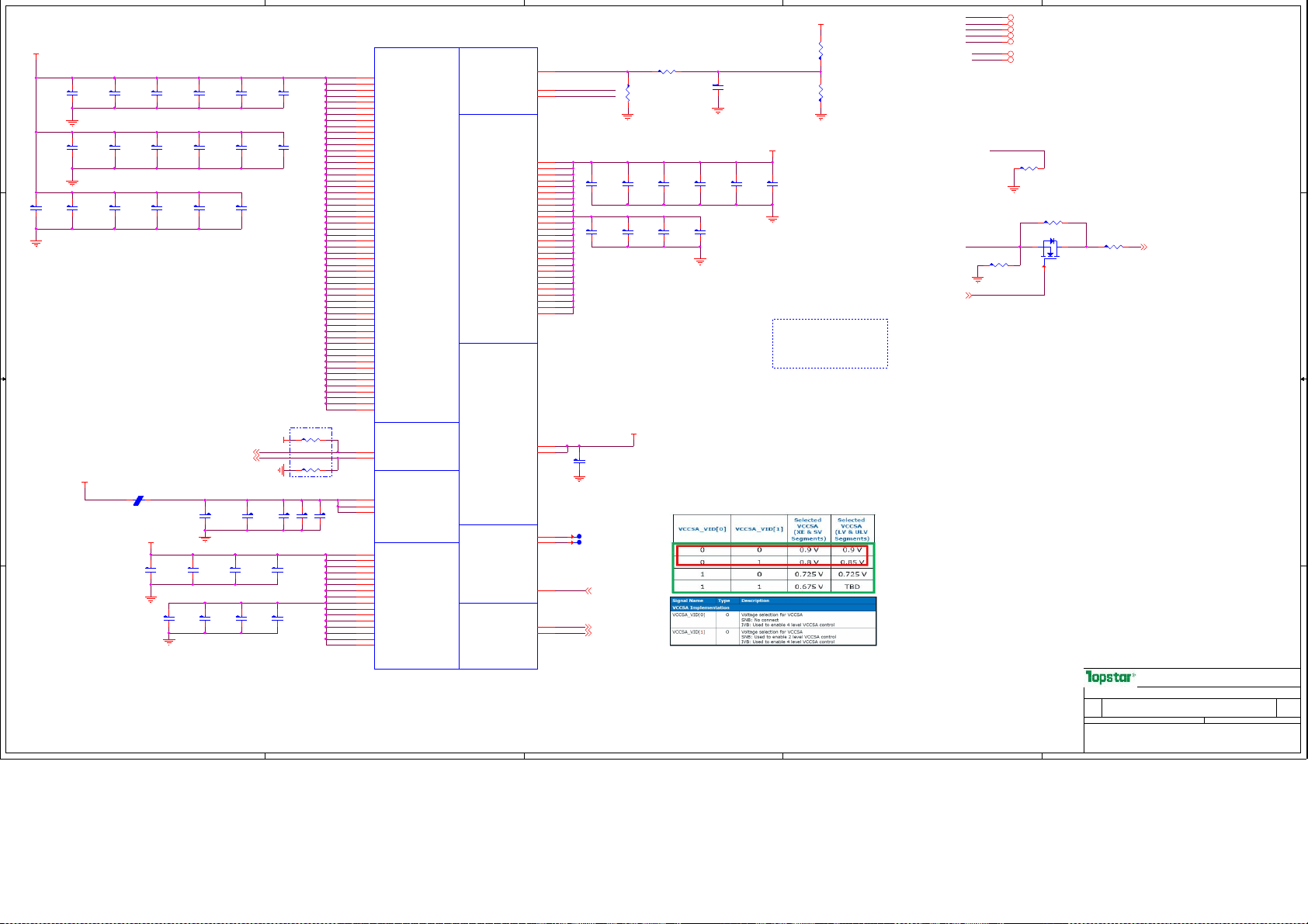
VCCSA VID
SM_VREF
SA_DIMM_VREFDQ
SB_DIMM_VREFDQ
VDDQ[1]
VDDQ[2]
VDDQ[3]
VDDQ[4]
VDDQ[5]
VDDQ[6]
VDDQ[7]
VDDQ[8]
VDDQ[9]
VDDQ[10]
VDDQ[11]
VDDQ[12]
VDDQ[13]
VDDQ[14]
VDDQ[15]
VDDQ[16]
VDDQ[17]
VDDQ[18]
VDDQ[19]
VDDQ[20]
VDDQ[21]
VDDQ[22]
VDDQ[23]
VDDQ[24]
VDDQ[25]
VDDQ[26]
VCCDQ[1]
VCCDQ[2]
QUIET RAILS
VDDQ_SENSE
VSS_SENSE_VDDQ
VCCSA_SENSE
SENSE LINES
VCCSA_VID[0]
VCCSA_VID[1]
lines
3
AY43
BE7
DDR_WR_VREF0 1
BG7
DDR_WR_VREF0 2
AJ28
AJ33
AJ36
AJ40
AL30
AL34
AL38
AL42
AM33
AM36
AM40
AN30
AN34
AN38
AR26
AR28
AR30
AR32
AR34
AR36
AR40
AV41
AW26
BA40
BB28
BG33
AM28
AN26
BC43
BA43
U10
D48
D49
VID0:For Sandy Bridge processor the
output will be low, for Ivy Bridge processor the output will be high.
VID1:For Chief River platforms, this
pin must have a pull down resistor to ground.
CRB 8颗10uF,10颗1uF,1颗330uF
C174
C0805
10uf/6.3 V
C474
C0805
10uf/6.3 V
0.6A
C128
C0402
1uf/10V
T79 ICTP ns
T85 ICTP ns
VCCSA_SENSE 42
VCCSA_SELECT0 4 2
VCCSA_SELECT1 4 2
+V1.5S
R282 0 R04 02
R255
100K
R0402
ns
C175
C0805
10uf/6.3 V
C475
C0805
10uf/6.3 V
C178
C0402
0.1uF/1 0V,X7R
+V1.5S
Max: 5A
C167
C0402
1uf/10V
C477
C0805
10uf/6.3 V
C166
C0402
1uf/10V
TU142 VerB: Changed 0 ohm to open point for cost down 2011-12-20
CL341 VerC: Remove the open jump 1227
C168
C0402
1uf/10V
C476
C0805
10uf/6.3 V
差异
3:VCCSA_SEL[1:0] pins enable dynamic selection
3
SM_VREF_RSM_VREF
1uf/10V
C163
C0402
+V1.5S
R270
1K,1%
R0402
R269
1K,1%
R0402
2
DDR_WR_VREF0 2
DRAMRST_CNTRL7
2
DDR_WR_VREF0 1
R731 1K
R0402
DRAMRST_CNTRL
R728 1K
ns
+V1.5 7,14,40,45
+V1.5S_CPU_VDDQ
+VCCSA 42
+VDC 2 4,37,39,40 ,41,44,47
+VGFX 44
+V1.5S 7,21,31,45
+V1.8S 20,21,40,45
ns
R0402
R729 0 R0 402
ns
3
2
Q39
L2N7002LT 1G
SOT23
1
Page Name
Page Name
Page Name
Size
Size
Size
Date: Sheet of
Date: Sheet of
Date: Sheet of
PROPERTY NOTE: th is document con tains informatio n confidentia l and prop erty to
PROPERTY NOTE: th is document con tains informatio n confidentia l and prop erty to
PROPERTY NOTE: th is document con tains informatio n confidentia l and prop erty to
TOPSTAR an d shall not b e reprodu ced or tran sferred to other docu ments or disclos ed
TOPSTAR an d shall not b e reprodu ced or tran sferred to other docu ments or disclos ed
TOPSTAR an d shall not b e reprodu ced or tran sferred to other docu ments or disclos ed
to other s or used fo r any purp ose other t han that fo r which it was obtaine d without
to other s or used fo r any purp ose other t han that fo r which it was obtaine d without
to other s or used fo r any purp ose other t han that fo r which it was obtaine d without
the expresse d written conse nt of TOPSTAR
the expresse d written conse nt of TOPSTAR
the expresse d written conse nt of TOPSTAR
R730 0
R0402
Project Name Rev
Project Name Rev
Project Name Rev
Custom
Custom
Custom
1
DDR_WR_VREF0 1_D1 14
TOPSTAR T ECHNOLOGY
TOPSTAR T ECHNOLOGY
TOPSTAR T ECHNOLOGY
Robin
Robin
Robin
Ivy Bridge VGF X/VDDQ
Ivy Bridge VGF X/VDDQ
Ivy Bridge VGF X/VDDQ
CL42 EVT
CL42 EVT
CL42 EVT
1
A
A
10 51Wednesda y, January 09, 2013
10 51Wednesda y, January 09, 2013
10 51Wednesda y, January 09, 2013
A
Page 11
5
U16H
A13
VSS [1]
A17
VSS [2]
A21
VSS [3]
A25
VSS [4]
A28
VSS [5]
A33
VSS [6]
A37
VSS [7]
D D
C C
B B
A40
A45
A49
A53
AA1
AA1 3
AA5 0
AA5 1
AA5 2
AA5 3
AA5 5
AA5 6
AA8
AB1 6
AB1 8
AB2 1
AB4 8
AB6 1
AC1 0
AC1 4
AC4 6
AC6
AD1 7
AD2 0
AD4
AD6 1
AE1 3
AE8
AF1
AF1 7
AF2 1
AF4 7
AF4 8
AF5 0
AF5 1
AF5 2
AF5 3
AF5 5
AF5 6
AF5 8
AF5 9
AG1 0
AG1 4
AG1 8
AG4 7
AG5 2
AG6 1
AG7
AH4
AH58
AJ1 3
AJ1 6
AJ2 0
AJ2 2
AJ2 6
AJ3 0
AJ3 4
AJ3 8
AJ4 2
AJ4 5
AJ4 8
AJ7
AK1
AK5 2
AL1 0
AL1 3
AL1 7
AL2 1
AL2 5
AL2 8
AL3 3
AL3 6
AL4 0
AL4 3
AL4 7
AL6 1
AM13
AM20
AM22
AM26
AM30
AM34
VSS [8]
VSS [9]
VSS [10]
VSS [11]
A9
VSS [12]
VSS [13]
VSS [14]
VSS [15]
VSS [16]
VSS [17]
VSS [18]
VSS [19]
VSS [20]
VSS [21]
VSS [22]
VSS [23]
VSS [24]
VSS [25]
VSS [26]
VSS [27]
VSS [28]
VSS [29]
VSS [30]
VSS [31]
VSS [32]
VSS [33]
VSS [34]
VSS [35]
VSS [36]
VSS [37]
VSS [38]
VSS [39]
VSS [40]
VSS [41]
VSS [42]
VSS [43]
VSS [44]
VSS [45]
VSS [46]
VSS [47]
VSS [48]
VSS [49]
VSS [50]
VSS [51]
VSS [52]
VSS [53]
VSS [54]
VSS [55]
VSS [56]
VSS [57]
VSS [58]
VSS [59]
VSS [60]
VSS [61]
VSS [62]
VSS [63]
VSS [64]
VSS [65]
VSS [66]
VSS [67]
VSS [68]
VSS [69]
VSS [70]
VSS [71]
VSS [72]
VSS [73]
VSS [74]
VSS [75]
VSS [76]
VSS [77]
VSS [78]
VSS [79]
VSS [80]
VSS [81]
VSS [82]
VSS [83]
VSS [84]
VSS [85]
VSS [86]
VSS [87]
VSS [88]
VSS [89]
VSS [90]
4
VSS
VSS [91]
VSS [92]
VSS [93]
VSS [94]
VSS [95]
VSS [96]
VSS [97]
VSS [98]
VSS [99]
VSS [100]
VSS [101]
VSS [102]
VSS [103]
VSS [104]
VSS [105]
VSS [106]
VSS [107]
VSS [108]
VSS [109]
VSS [110]
VSS [111]
VSS [112]
VSS [113]
VSS [114]
VSS [115]
VSS [116]
VSS [117]
VSS [118]
VSS [119]
VSS [120]
VSS [121]
VSS [122]
VSS [123]
VSS [124]
VSS [125]
VSS [126]
VSS [127]
VSS [128]
VSS [129]
VSS [130]
VSS [131]
VSS [132]
VSS [133]
VSS [134]
VSS [135]
VSS [136]
VSS [137]
VSS [138]
VSS [139]
VSS [140]
VSS [141]
VSS [142]
VSS [143]
VSS [144]
VSS [145]
VSS [146]
VSS [147]
VSS [148]
VSS [149]
VSS [150]
VSS [151]
VSS [152]
VSS [153]
VSS [154]
VSS [155]
VSS [156]
VSS [157]
VSS [158]
VSS [159]
VSS [160]
VSS [161]
VSS [162]
VSS [163]
VSS [164]
VSS [165]
VSS [166]
VSS [167]
VSS [168]
VSS [169]
VSS [170]
VSS [171]
VSS [172]
VSS [173]
VSS [174]
VSS [175]
VSS [176]
VSS [177]
VSS [178]
VSS [179]
VSS [180]
AM38
AM4
AM42
AM45
AM48
AM58
AN1
AN21
AN25
AN28
AN33
AN36
AN40
AN43
AN47
AN50
AN54
AP1 0
AP5 1
AP5 5
AP7
AR1 3
AR1 7
AR2 1
AR4 1
AR4 8
AR6 1
AR7
AT1 4
AT1 9
AT3 6
AT4
AT4 5
AT5 2
AT5 8
AU1
AU11
AU28
AU32
AU51
AU7
AV1 7
AV2 1
AV2 2
AV3 4
AV4 0
AV4 8
AV5 5
AW 13
AW 43
AW 61
AW 7
AY14
AY19
AY30
AY36
AY4
AY41
AY45
AY49
AY55
AY58
AY9
BA1
BA1 1
BA1 7
BA2 1
BA2 6
BA3 2
BA4 8
BA5 1
BB5 3
BC1 3
BC5
BC5 7
BD1 2
BD1 6
BD1 9
BD2 3
BD2 7
BD3 2
BD3 6
BD4 0
BD4 4
BD4 8
BD5 2
BD5 6
BD8
BE5
BG1 3
3
U16I
BG1 7
VSS [181]
BG2 1
VSS [182]
BG2 4
VSS [183]
BG2 8
VSS [184]
BG3 7
VSS [185]
BG4 1
VSS [186]
BG4 5
VSS [187]
BG4 9
VSS [188]
BG5 3
VSS [189]
BG9
VSS [190]
C29
VSS [191]
C35
VSS [192]
C40
VSS [193]
D10
VSS [194]
D14
VSS [195]
D18
VSS [196]
D22
VSS [197]
D26
VSS [198]
D29
VSS [199]
D35
VSS [200]
D4
VSS [201]
D40
VSS [202]
D43
VSS [203]
D46
VSS [204]
D50
VSS [205]
D54
VSS [206]
D58
VSS [207]
D6
VSS [208]
E25
VSS [209]
E29
VSS [210]
E3
VSS [211]
E35
VSS [212]
E40
VSS [213]
F13
VSS [214]
F15
VSS [215]
F19
VSS [216]
F29
VSS [217]
F35
VSS [218]
F40
VSS [219]
F55
VSS [220]
G51
VSS [221]
G6
VSS [222]
G61
VSS [223]
H10
VSS [224]
H14
VSS [225]
H17
VSS [226]
H21
VSS [227]
H4
VSS [228]
H53
VSS [229]
H58
VSS [230]
J1
VSS [231]
J49
VSS [232]
J55
VSS [233]
K11
VSS [234]
K21
VSS [235]
K51
VSS [236]
K8
VSS [237]
L16
VSS [238]
L20
VSS [239]
L22
VSS [240]
L26
VSS [241]
L30
VSS [242]
L34
VSS [243]
L38
VSS [244]
L43
VSS [245]
L48
VSS [246]
L61
VSS [247]
M11
VSS [248]
M15
VSS [249]
IC,IVB_2CBGA,0P7
BGA1023_31X24
VSS
NCTF
VSS [250]
VSS [251]
VSS [252]
VSS [253]
VSS [254]
VSS [255]
VSS [256]
VSS [257]
VSS [258]
VSS [259]
VSS [260]
VSS [261]
VSS [262]
VSS [263]
VSS [264]
VSS [265]
VSS [266]
VSS [267]
VSS [268]
VSS [269]
VSS [270]
VSS [271]
VSS [272]
VSS [273]
VSS [274]
VSS [275]
VSS [276]
VSS [277]
VSS [278]
VSS [279]
VSS [280]
VSS [281]
VSS [282]
VSS [283]
VSS [284]
VSS [285]
VSS [286]
VSS [287]
VSS [288]
VSS [289]
VSS [290]
VSS [291]
VSS [292]
VSS [293]
VSS [294]
VSS [295]
VSS [296]
VSS [297]
VSS [298]
VSS [299]
VSS [300]
VSS _NCTF_1
VSS _NCTF_2
VSS _NCTF_3
VSS _NCTF_4
VSS _NCTF_5
VSS _NCTF_6
VSS _NCTF_7
VSS _NCTF_8
VSS _NCTF_9
VSS _NCTF_1 0
VSS _NCTF_1 1
VSS _NCTF_1 2
VSS _NCTF_1 3
VSS _NCTF_1 4
2
M4
M58
M6
N1
N17
N21
N25
N28
N33
N36
N40
N43
N47
N48
N51
N52
N56
N61
P14
P16
P18
P21
P58
P59
P9
R17
R20
R4
R46
T1
T47
T50
T51
T52
T53
T55
T56
U13
U8
V20
V61
W1 3
W1 5
W1 8
W2 1
W4 6
W8
Y4
Y47
Y58
Y59
A5
A57
BC6 1
BD3
BD5 9
BE4
BE5 8
BG5
BG5 7
C3
C58
D59
E1
E61
1
A A
5
IC,IVB_2CBGA,0P7
BGA1023_31X24
Page Name
Page Name
Page Name
Size
Size
Size
Project Name Rev
Project Name Rev
Project Name Rev
A3
A3
A3
Date: Sheet of
Date: Sheet of
Date: Sheet of
PROPERTY NOTE: this document contains information confidential and property to
PROPERTY NOTE: this document contains information confidential and property to
PROPERTY NOTE: this document contains information confidential and property to
TOPSTAR and shall not be reproduced or transferred to other documents or disclosed
TOPSTAR and shall not be reproduced or transferred to other documents or disclosed
TOPSTAR and shall not be reproduced or transferred to other documents or disclosed
to others or used for any purpose other than that for which it was obtained without
to others or used for any purpose other than that for which it was obtained without
to others or used for any purpose other than that for which it was obtained without
the expressed written consent of TOPSTAR
the expressed written consent of TOPSTAR
the expressed written consent of TOPSTAR
4
3
2
TOPSTAR TECHNOLOGY
TOPSTAR TECHNOLOGY
TOPSTAR TECHNOLOGY
Robin
Robin
Robin
Ivy Bridge GND
Ivy Bridge GND
Ivy Bridge GND
CL42 EVT
CL42 EVT
CL42 EVT
1
A
A
11 51Wednesday, January 09, 2013
11 51Wednesday, January 09, 2013
11 51Wednesday, January 09, 2013
A
Page 12
5
4
3
2
1
U16E
B50
CFG[0]
C51
CFG[1]
B54
CFG[2]
D53
CFG[3]
A51
D D
C C
BRACKET1
CPU_HOLE
ASSY
B B
1122334455667788991010111112121313141415151616171718181919202021212222232324242525262627272828292930303131323233333434353536
36
A A
5
4
CFG[4]
C53
CFG[5]
C55
CFG[6]
H49
CFG[7]
A55
CFG[8]
H51
CFG[9]
K49
CFG[10]
K53
CFG[11]
F53
CFG[12]
G53
CFG[13]
L51
CFG[14]
F51
CFG[15]
D52
CFG[16]
L53
CFG[17]
H43
VCC_VAL_SENSE
K43
VSS_VAL_SENSE
H45
VAXG_VAL_SENSE
K45
VSSAXG_VAL_SENSE
F48
VCC_DIE_SENSE
G48
RSVD47
H48
RSVD6
K48
RSVD7
BA19
RSVD8
AV19
RSVD9
AT21
RSVD10
BB21
RSVD11
BB19
RSVD12
AY21
RSVD13
BA22
RSVD14
AY22
RSVD15
AU19
RSVD16
AU21
RSVD17
BD21
RSVD18
BD22
RSVD19
BD25
RSVD20
BD26
RSVD21
BG22
RSVD22
BE22
RSVD23
BG26
RSVD24
BE26
RSVD25
BF23
RSVD26
BE24
RSVD27
IC,IVB_2CBGA,0P7
BGA1023_31X24
RESERVED
3
BCLK_ITP
BCLK_ITP#
RSVD30
RSVD31
RSVD32
RSVD33
RSVD34
RSVD35
RSVD36
RSVD37
RSVD38
RSVD39
RSVD40
RSVD41
RSVD42
RSVD43
RSVD44
RSVD45
DC_TEST_A4
DC_TEST_C4
DC_TEST_D3
DC_TEST_D1
DC_TEST_A58
DC_TEST_A59
DC_TEST_C59
DC_TEST_A61
DC_TEST_C61
DC_TEST_D61
DC_TEST_BD61
DC_TEST_BE61
DC_TEST_BE59
DC_TEST_BG61
DC_TEST_BG59
DC_TEST_BG58
DC_TEST_BG4
DC_TEST_BG3
DC_TEST_BE3
DC_TEST_BG1
DC_TEST_BE1
DC_TEST_BD1
N59
ns
N58
N42
L42
L45
L47
M13
M14
U14
W14
P13
AT49
K24
AH2
AG13
AM14
AM15
T70
T71
ICTP
ICTP
ns
N50
A4
DC_TEST_A4
C4
D3
DC_TEST_C4_D3
D1
DC_TEST_D1
A58
DC_TEST_A58
A59
C59
DC_TEST_A59_C59
A61
C61
DC_TEST_A61_C61
D61
DC_TEST_D61
BD61
DC_TEST_BD61
BE61
BE59
DC_TEST_BE59_BE61
BG61
BG59
DC_TEST_BG59_BG61
BG58
DC_TEST_BG58
BG4
DC_TEST_BG4
BG3
BE3
DC_TEST_BE3_BG3
BG1
BE1
DC_TEST_BE1_BG1
BD1
DC_TEST_BD1
Daisy Chain, for solder joint reliability
and non-critical to function. BGA only.
Followed CRB connection.
TOPSTAR TECHNOLOGY
TOPSTAR TECHNOLOGY
TOPSTAR TECHNOLOGY
Robin
Robin
Robin
Page Name
Page Name
Page Name
Size
Size
Size
Project Name Rev
Project Name Rev
Project Name Rev
A4
A4
A4
Date: Sheet of
Date: Sheet of
Date: Sheet of
PROPERTY NOTE: this document contains information confidential and property to
PROPERTY NOTE: this document contains information confidential and property to
PROPERTY NOTE: this document contains information confidential and property to
TOPSTAR and shall not be reproduced or transferred to other documents or disclosed
TOPSTAR and shall not be reproduced or transferred to other documents or disclosed
TOPSTAR and shall not be reproduced or transferred to other documents or disclosed
to others or used for any purpose other than that for which it was obtained without
to others or used for any purpose other than that for which it was obtained without
to others or used for any purpose other than that for which it was obtained without
the expressed written consent of TOPSTAR
the expressed written consent of TOPSTAR
the expressed written consent of TOPSTAR
2
Ivy Bridge Reserved
Ivy Bridge Reserved
Ivy Bridge Reserved
CL42 EVT
CL42 EVT
CL42 EVT
12 51Wednesday, January 09, 2013
12 51Wednesday, January 09, 2013
12 51Wednesday, January 09, 2013
1
A
A
A
Page 13

5
D D
C C
4
3
2
1
B B
A A
Page Name
Page Name
Page Name
Size
Size
Size
Project Name Rev
Project Name Rev
Project Name Rev
A3
A3
A3
Date: Sheet of
Date: Sheet of
Date: Sheet of
PROPERTY NOTE: this document contains information confidential and property to
PROPERTY NOTE: this document contains information confidential and property to
PROPERTY NOTE: this document contains information confidential and property to
TOPSTAR and shall not be reproduced or transferred to other documents or disclosed
TOPSTAR and shall not be reproduced or transferred to other documents or disclosed
TOPSTAR and shall not be reproduced or transferred to other documents or disclosed
to others or used for any purpose other than that for which it was obtained without
to others or used for any purpose other than that for which it was obtained without
to others or used for any purpose other than that for which it was obtained without
the expressed written consent of TOPSTAR
the expressed written consent of TOPSTAR
the expressed written consent of TOPSTAR
5
4
3
2
TOPSTAR TECHNOLOGY
TOPSTAR TECHNOLOGY
TOPSTAR TECHNOLOGY
杨华明
(Sky Yang)
杨华明
(Sky Yang)
杨华明
(Sky Yang)
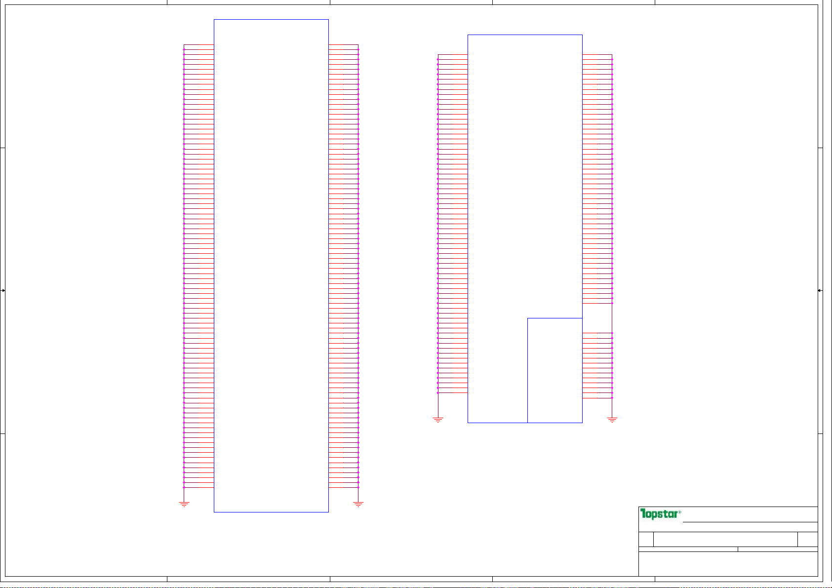
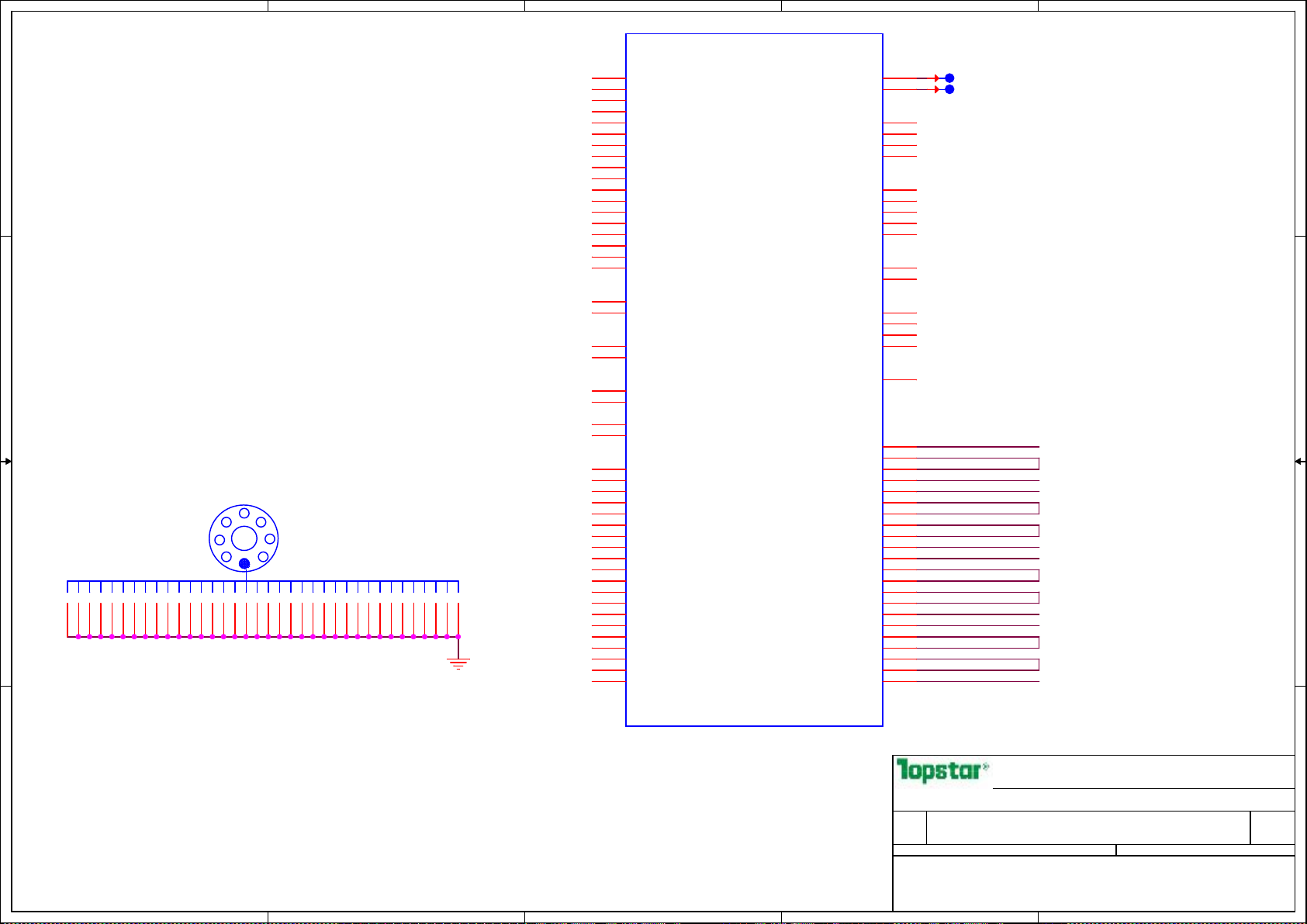
DDR3 CHA SODIMM0
DDR3 CHA SODIMM0
DDR3 CHA SODIMM0
CL42 EVT
CL42 EVT
CL42 EVT
1
A
A
13 51Wednesday, January 09, 2013
13 51Wednesday, January 09, 2013
13 51Wednesday, January 09, 2013
A
Page 14
+V1.5
5
4
3
2
+V3.3S 7,15,16,17,18,19,20,21,22,24,25,29,30,31,32,33,34,35,40,41,42,43,44,45,47
+V1.5 7,40,45
+V0.75S 40,45
1
2.2uf/10V
2.2uf/10V
1uf/10V
+V1.5
C217
C0603
C218
C0603
ns
C193
C0402
R303
1K,1%
R0402
C192
C0402
0.1UF/10V,X7R
ns
公版6颗
10uF,1颗330uF,4颗1uF
C216
C0402
0.1UF/10V,X7R
电容靠近
C227
C0402
1uf/10V
2.2uf/10V
2.2uf/10V
DDR slot VDD PIN
1uf/10V
C237
C0805
10uf/6.3V
D D
+V1.5
C235
C0402
0.1UF/10V,X7R
C C
B B
Layout note:
+V0.75S
C198
C0402
1uf/10V
C242
C0603
C220
C0603
C224
C0402
C241
C0603
2.2uf/10V
C184
C0603
2.2uf/10V
ns
+V1.5
VREFB_CA
R312
1K,1%
R0402
R310
1K,1%
R0402
C187
C0402
0.1UF/10V,X7R
ns
C234
C0402
0.1UF/10V,X7R
ns
DDR_WR_VREF01_D1
C238
C0603
2.2uf/10V
C214
C0603
2.2uf/10V
ns
C239
C0603
2.2uf/10V
C215
C0603
2.2uf/10V
C228
C0402
0.1UF/10V,X7R
+V3.3S
C236
C0402
0.1UF/10V,X7R
C203
10uf/6.3V
C0805
C226
C0603
2.2uf/10V
C219
10uf/6.3V
C0805
DDR_WR_VREF01_D110
MB_B_A[15:0]8
MB_B_BS08
MB_B_BS18
MB_B_BS28
M_CS#28
M_CS#38
MB_B_WE#8
MB_B_CAS#8
MB_B_RAS#8
M_CKE28
M_CKE38
M_CLK_DDR28
M_CLK_DDR#28
M_CLK_DDR38
M_CLK_DDR#38
M_ODT28
M_ODT38
MB_DQS[7:0]8
SMB_DATA_S16
SMB_CLK_S16
R318 10K R0402
R316 10K R0402
Note:
SO-DIMM1 SPD Address is 0xA4
C230
C0402
0.1UF/10V,X7R
DDR3_DRAMRST#7
C229
C0603
2.2uf/10V
MB_B_A0
MB_B_A1
MB_B_A2
MB_B_A3
MB_B_A4
MB_B_A5
MB_B_A6
MB_B_A7
MB_B_A8
MB_B_A9
MB_B_A10
MB_B_A11
MB_B_A12
MB_B_A13
MB_B_A14
MB_B_A15
MB_DQS0
MB_DQS1
MB_DQS2
MB_DQS3
MB_DQS4
MB_DQS5
MB_DQS6
MB_DQS7
VREFB_CA
+V1.5+V0.75S
203
204
VTT1
VTT2
98
A0
97
A1
96
A2
95
A3
92
A4
91
A5
90
A6
86
A7
89
A8
85
A9
107
A10 /AP
84
A11
83
A12 /BC#
119
A13
80
A14
78
A15
109
BA0
108
BA1
79
BA2
114
CS0
121
CS1
11
DQM0
28
DQM1
46
DQM2
63
DQM3
136
DQM4
153
DQM5
170
DQM6
187
DQM7
113
WE
115
CAS
110
RAS
73
CKE 0
74
CKE 1
101
CK0
103
CK0
102
CK1
104
CK1
116
ODT 0
120
ODT 1
12
DQS 0
29
DQS 1
47
DQS 2
64
DQS 3
137
DQS 4
154
DQS 5
171
DQS 6
188
DQS 7
200
SDA
202
SCL
197
SA0
201
SA1
199
VDD SPD
1
VRE F_DQ
126
VRE F_CA
198
EVE NT#
30
RES ET#
77
NC1
122
NC2
125
NCTE ST
DDR3_SODIMM204_0
99
100
105
106
111
112
117
118
VDD175VDD276VDD381VDD482VDD587VDD688VDD793VDD894VDD9
VSS23VSS38VSS49VSS513VSS614VSS719VSS820VSS925VSS1026VSS1131VSS1232VSS1337VSS1438VSS1543VSS1644VSS1748VSS1849VSS1954VSS2055VSS2160VSS2261VSS2365VSS2466VSS2571VSS2672VSS27
VSS1
VDD10
VDD11
VDD12
VDD13
VDD14
VDD15
151
145
150
123
VDD16
155
124
VSS36
VSS34
VSS35
VDD17
VDD18
2
156
161
162
167
168
172
173
178
179
184
185
189
190
195
196
DIMM1
5
VSS37
VSS38
VSS39
VSS40
VSS41
VSS42
VSS43
VSS44
VSS45
VSS46
VSS47
VSS48
VSS49
VSS50
VSS51
D0
D1
D2
D3
D4
D5
D6
D7
D8
D9
D10
D11
D12
D13
D14
D15
D16
D17
D18
D19
D20
D21
D22
D23
D24
D25
D26
D27
D28
D29
D30
D31
D32
D33
D34
D35
D36
D37
D38
D39
D40
D41
D42
D43
D44
D45
D46
D47
D48
D49
D50
D51
D52
D53
D54
D55
D56
D57
D58
D59
D60
D61
D62
D63
DQS #0
DQS #1
DQS #2
DQS #3
DQS #4
DQS #5
DQS #6
DQS #7
VSS29
VSS30
VSS31
VSS32
VSS28
VSS33
GND1
GND2
127
133
134
138
139
128
144
205
206
MB_DATA0
VSS52
7
MB_DATA1
15
MB_DATA2
17
MB_DATA3
4
MB_DATA4
6
MB_DATA5
16
MB_DATA6
18
MB_DATA7
21
MB_DATA8
23
MB_DATA9
33
MB_DATA10
35
MB_DATA11
22
MB_DATA12
24
MB_DATA13
34
MB_DATA14
36
MB_DATA15
39
MB_DATA16
41
MB_DATA17
51
MB_DATA18
53
MB_DATA19
40
MB_DATA20
42
MB_DATA21
50
MB_DATA22
52
MB_DATA23
57
MB_DATA24
59
MB_DATA25
67
MB_DATA26
69
MB_DATA27
56
MB_DATA28
58
MB_DATA29
68
MB_DATA30
70
MB_DATA31
129
MB_DATA32
131
MB_DATA33
141
MB_DATA34
143
MB_DATA35
130
MB_DATA36
132
MB_DATA37
140
MB_DATA38
142
MB_DATA39
147
MB_DATA40
149
MB_DATA41
157
MB_DATA42
159
MB_DATA43
146
MB_DATA44
148
MB_DATA45
158
MB_DATA46
160
MB_DATA47
163
MB_DATA48
165
MB_DATA49
175
MB_DATA50
177
MB_DATA51
164
MB_DATA52
166
MB_DATA53
174
MB_DATA54
176
MB_DATA55
181
MB_DATA56
183
MB_DATA57
191
MB_DATA58
193
MB_DATA59
180
MB_DATA60
182
MB_DATA61
192
MB_DATA62
194
MB_DATA63
10
MB_DQS#0
27
MB_DQS#1
45
MB_DQS#2
62
MB_DQS#3
135
MB_DQS#4
152
MB_DQS#5
169
MB_DQS#6
186
MB_DQS#7
MB_DATA[63:0] 8
MB_DQS#[7:0] 8
R302
A A
1K,1%
R0402
5
C213
C0402
0.1UF/10V,X7R
C222
C0603
2.2uf/10V
TOPSTAR TECHNOLOGY
TOPSTAR TECHNOLOGY
TOPSTAR TECHNOLOGY
杨华明
(Sky Yang)
杨华明
(Sky Yang)
杨华明
Page Name
Page Name
Page Name
Size
Size
Size
Project Name Rev
Project Name Rev
Project Name Rev
A3
A3
A3
Date: Sheet of
Date: Sheet of
Date: Sheet of
PROPERTY NOTE: this document contains information confidential and property to
PROPERTY NOTE: this document contains information confidential and property to
PROPERTY NOTE: this document contains information confidential and property to
TOPSTAR and shall not be reproduced or transferred to other documents or disclosed
TOPSTAR and shall not be reproduced or transferred to other documents or disclosed
TOPSTAR and shall not be reproduced or transferred to other documents or disclosed
to others or used for any purpose other than that for which it was obtained without
to others or used for any purpose other than that for which it was obtained without
to others or used for any purpose other than that for which it was obtained without
the expressed written consent of TOPSTAR
the expressed written consent of TOPSTAR
the expressed written consent of TOPSTAR
4
3
2
(Sky Yang)
DDR3 CHB SODIMM0
DDR3 CHB SODIMM0
DDR3 CHB SODIMM0
CL42 EVT
CL42 EVT
CL42 EVT
1
A
A
14 51Wednesday, January 09, 2013
14 51Wednesday, January 09, 2013
14 51Wednesday, January 09, 2013
A
Page 15
5
EC_RTC
D D
3
1
3
1
2
2
4
RTCCN1
4
Wafer
CNS2_V
HDA_SYNC:On-Die PLL Voltage Regulator Voltage Select
(Internal pull down 20K)
Low: 1.8V
High: 1.5V(Default)
C C
AZALIA_CODEC_SYNC29
VerC:HDA_SDO:
B B
A A
增加对声卡芯片的隔离电路,防止刷写ME是EC无法在S5下将
AZALIA_CODEC_SDOUT29
R0402
R334
1K
R0402
+V3.3S
R442
R0402
0
KB3930
D1
LBAT54CLT1G
sot23
1
3
2
+V3.3S
R706
1K
R0402
ns
R707 33 R0402
R708
1M
R0402
+V3.3S
R716
1K
R0402
R717 33 R0402
+V3.3SB
R440
R0402
0
KB9010
R444 10K R0402 ns
R447 3.3K R0402
R439 3.3K R0402
R718
1M
R0402
ns
R22
1M
R0402
8
3
7
PCH_EC_RTC
R24 20K R0402
R26 20K R0402
R705 0
Q36
L2N7002LT1G
2
+V5S
1
ME_LOCK#
+V5S
U13
VDD
CE#
WP #
SCK
HOLD#
VSS
W25Q32BVSSIG
SOIC8_50_208
C294
1uf/10V
C0402
C17
1uf/10V
C0402
nsR0402
3
SOT23
拉高
R715 0
Q37
L2N7002LT1G
2
SOT23
1
5
SI
2
SO
1
6
4
CMOS Settings J1
Clear CMOS Short
Keep CMOS Open
C16
1uf/10V
C0402
Pull High to enable
internal SUS1.05V VR
HDA_SYNC
nsR0402
3
Boot BIOS Strap
GNT1# SATA1GP Boot BIOS Location
0 0
0 1
1 0
1 1
LPC
Reserved
PCI
SPI
5
RTC_BAT1
12
J1
JOPEN
RESISTOR_1
ns
HDA_SDO
PCH_SPI_MOSI_Q
PCH_SPI_MISO_Q
PCH_SPI_CS0#_Q
PCH_SPI_CLK_Q
EC_OWNER33
4
+
-
RTCBAT with Cable
ASSYR1 1K
C292
C0402
15pF/50V,NPO
C296
PCH_EC_RTC
AZALIA_CODEC_BITCLK29
AZALIA_CODEC_RST#29
HDA_SDO:Flash Descriptor Security Overide
Internal pull down 20K
Low = Disabled(Default)
High = Enabled
EC_ME_LOCK#33
PCH_SPI_MOSI_Q
PCH_SPI_MISO_Q
PCH_SPI_CS0#_Q
PCH_SPI_CLK_Q
PCH_SPI_MOSI_Q
PCH_SPI_CS0#_Q
4
+V3.3AL
SPKR29
AZALIA_SDATAIN029
+V3.3AL
PCH_SPI_MOSI_Q 33
PCH_SPI_MISO_Q 33
PCH_SPI_CS0#_Q 33
PCH_SPI_CLK_Q 33
+V3.3SB
R183
4.7K
R0402
KB9010
R202
4.7K
R0402
KB9010
+V3.3SB
R377 0
R0402
Y1
3
xd3
ASSY
32.768KHz
1 2
15pF/50V,NPOC0402
R372 332K,1%
R46 33 R0402
R34 1K R0402
R44 33 R0402
R390 1K R0402
R294
4.7K
R0402
ns
R0402
ns
ICTP ns
ICTP ns
ICTP ns
ICTP ns
RTC_RST#
SRTC_RST#
SM_INTRUDER#
ICH_INTVRMEN
T36
T9
T13
T37
Internal pull high for no use
R412 place close to PCH in 500mils
R724 0 KB3930R0402
EC_OWNER
Q8
SC70_6
6
3 4
KB9010
EC_OWNER
2
1
5
L2N7002DW1T1G
R733 0 KB3930R0402
32XCLK0
R394
10M
R0402
32XCLK1
HDA_BCLK
HDA_SYNC
HDA_RST#
Internal PD20K
HDA_SDO
R374 4.7K R0402
ns
PCH_SPI_CLK
PCH_SPI_CS0#
PCH_SPI_MOSI
PCH_SPI_MISO
+V3.3S
R186
4.7K
R0402
KB9010
PCH_SPI_MOSI
PCH_SPI_CS0#
R203
4.7K
R0402
KB9010
+V3.3S
3
U12A
A20
RTC X1
C20
RTC X2
D20
RTC RST#
G22
SRT CRST#
K22
INTR UDER#
C17
INTV RMEN
N34
HDA_B CLK
L34
HDA_S YNC
T10
SPK R
K34
HDA_R ST#
E34
HDA_S DIN0
G34
HDA_S DIN1
C34
HDA_S DIN2
A34
HDA_S DIN3
A36
HDA_S DO
C36
HDA_D OCK_E N# / GPIO3 3
N32
HDA_D OCK_R ST# / GPI O13
J3
JTA G_TCK
H7
JTA G_TMS
K5
JTA G_TDI
H1
JTA G_TDO
T3
SPI _CLK
Y14
SPI _CS0#
T1
SPI _CS1#
V4
SPI _MOSI
U3
SPI _MISO
CPT_PPT_Rev_0p5
3
R188
R0402
KB9010
PCH_SPI_MISO_Q
PCH_SPI_CLK_Q
R200
4.7K
R0402
KB9010
PCH_EC_RTC 17,22
EC_RTC 27,39,45
+V3.3S 7,14,16,17,18,19,20,21,22,24,25,29,30,31,32,33,34,35,40,41,42,43,44,45,47
+V3.3AL 7,16,17,19,20,22,24,28,31,33,40,43,45
+V1.05S 6,7,9,16,17,21,22,30,41,44,47
+V5S 16,22,24,25,27,28,29,30,40,42,44,45,47
+V3.3SB 7,17,20,22,28,31,33,35,37,38,39,45
FW H0 / LAD0
FW H1 / LAD1
FW H2 / LAD2
FW H3 / LAD3
LPC
FW H4 / LFRAME #
LDR Q0#
LDR Q1# / GPI O23
RTCIHDA
SATA 6G
SATA
SER IRQ
SAT A0RXN
SAT A0RXP
SAT A0TXN
SAT A0TXP
SAT A1RXN
SAT A1RXP
SAT A1TXN
SAT A1TXP
SAT A2RXN
SAT A2RXP
SAT A2TXN
SAT A2TXP
SAT A3RXN
SAT A3RXP
SAT A3TXN
SAT A3TXP
SAT A4RXN
SAT A4RXP
SAT A4TXN
SAT A4TXP
SAT A5RXN
SAT A5RXP
SAT A5TXN
SAT A5TXP
SAT AICOMPO
JTAG
SAT AICOMPI
SAT A3RCOMP O
SAT A3COMPI
SAT A3RBIA S
SPI
SAT ALED#
SAT A0GP / GP IO21
SAT A1GP / GP IO19
+V3.3SB
R727 0 KB3930R0402
4.7K
+V3.3SB
EC_OWNER
Q9
L2N7002DW1T1G
SC70_6
KB9010
EC_OWNER
R732 0 KB3930R0402
2
6
3 4
5
2
C38
A38
B37
C37
D36
E36
K36
Internal PU20K
V5
AM3
AM1
AP7
AP5
AM10
AM8
AP1 1
AP1 0
AD7
AD5
AH5
Port1/2/3 may not available in all SKUs
AH4
AB8
AB1 0
AF3
AF1
Y7
Y5
AD3
AD1
Y3
Y1
AB3
AB1
Y11
Y10
R108 37.4,1% R0402
LPC_AD0 31,33
LPC_AD1 31,33
LPC_AD2 31,33
LPC_AD3 31,33
LPC_FRAME# 31,33
INT_SERIRQ 33
SATA_RXN0 27
SATA_RXP0 27
SATA_TXN0 27
SATA_TXP0 27
NM70:only Port0 support 6Gb/s,port1/3 disable.
Port1/3 not available in HM70
SATA_RXN5 27
SATA_RXP5 27
SATA_TXN5 27
SATA_TXP5 27
AB1 2
AB1 3
AH1
R111 49.9,1% R0402
R438 750 OHM R0402
P3
V14
P1
1
R112 10K R0402
R418 10K R0402
Internal PU20K
+V3.3S
R192
4.7K
R0402
KB9010
PCH_SPI_MISO
PCH_SPI_CLK
R201
4.7K
R0402
KB9010
+V3.3S
2
1
+V1.05S
+V3.3S
+V3.3S
R422
R0402
10K
R23
10K
R0402
ns
INT_SERIRQ
+V3.3S
R63
10K
R0402
ns
SATA_LED#
+V3.3S
R103
10K
R0402
CRB pull up to 43K
TOPSTAR TECHNOLOGY
TOPSTAR TECHNOLOGY
TOPSTAR TECHNOLOGY
杨华明
(Sky Yang)
杨华明
(Sky Yang)
杨华明
Page Name
Page Name
Page Name
Size
Size
Size
Project Name Rev
Project Name Rev
Project Name Rev
A3
A3
A3
Date: Sheet of
Date: Sheet of
Date: Sheet of
PROPERTY NOTE: this document contains information confidential and property to
PROPERTY NOTE: this document contains information confidential and property to
PROPERTY NOTE: this document contains information confidential and property to
TOPSTAR and shall not be reproduced or transferred to other documents or disclosed
TOPSTAR and shall not be reproduced or transferred to other documents or disclosed
TOPSTAR and shall not be reproduced or transferred to other documents or disclosed
to others or used for any purpose other than that for which it was obtained without
to others or used for any purpose other than that for which it was obtained without
to others or used for any purpose other than that for which it was obtained without
the expressed written consent of TOPSTAR
the expressed written consent of TOPSTAR
the expressed written consent of TOPSTAR
(Sky Yang)
PCH RTC/SATA/SPI/HDA/LPC
PCH RTC/SATA/SPI/HDA/LPC
PCH RTC/SATA/SPI/HDA/LPC
CL42 EVT
CL42 EVT
CL42 EVT
1
15 51Wednesday, January 09, 2013
15 51Wednesday, January 09, 2013
15 51Wednesday, January 09, 2013
A
A
A
Page 16
5
PCIE_RXN1_LAN34
PCIE_RXP1_LAN34
PCIE_TXN1_LAN34
PCIE_TXP1_LAN34
D D
PCIE_RXN4_WLAN31
PCIE_RXP4_WLAN31
PCIE_TXN4_WLAN31
PCIE_TXP4_WLAN31
C76 0.1UF/10V,X7RC0402
C83 0.1UF/10V,X7RC0402
C90 0.1UF/10V,X7RC0402
C91 0.1UF/10V,X7RC0402
PCIE_TXN1_LAN_C
PCIE_TXP1_LAN_C
PCIE_TXN4_WLAN_C
PCIE_TXP4_WLAN_C
HM70/NM70 disable PCIE port 5/6/7/8
C C
PCIE_GLAN_CLKN34
PCIE_GLAN_CLKP34
+V3.3AL
+V3.3S
+V3.3S
B B
Note:
For free running clock, do not pull down REQ signal
to GND,this will increase leakage in Sx states.
A A
5
+V3.3AL
CLK_PCIE_MINICARD#31
CLK_PCIE_MINICARD31
minicard_CLKREQ#31
R401 10K
R0402
R411 10K
R0402
R104 10K R0402
R382 10K
R0402
R90 10K
R0402
R32 10K
R0402
R96 10K
R0402
R49 10K
R0402
R69 10K
R0402
PCIECLKRQ3#
PCIECLKRQ4#
PCIECLKRQ5#
PEG_B_CLKRQ#
PCIECLKRQ6#
PCIECLKRQ7#
4
BG3 4
BJ3 4
AV3 2
AU32
BE3 4
BF3 4
BB3 2
AY32
BG3 6
BJ3 6
AV3 4
AU34
BF3 6
BE3 6
AY34
BB3 4
BG3 7
BH37
AY36
BB3 6
BJ3 8
BG3 8
AU36
AV3 6
BG4 0
BJ4 0
AY40
BB4 0
BE3 8
BC3 8
AW 38
AY38
AB4 9
AB4 7
AA4 8
AA4 7
Internal PU20K
AB4 2
AB4 0
Internal PU20K
AK1 4
AK1 3
4
U12B
PER N1
PER P1
PET N1
PET P1
PER N2
PER P2
PET N2
PET P2
PER N3
PER P3
PET N3
PET P3
PER N4
PER P4
PET N4
PET P4
PER N5
PER P5
PET N5
PET P5
PER N6
PER P6
PET N6
PET P6
PER N7
PER P7
PET N7
PET P7
PER N8
PER P8
PET N8
PET P8
Y40
CLK OUT_PCI E0N
Y39
CLK OUT_PCI E0P
J2
PCI ECLKRQ 0# / GPIO 73
CLK OUT_PCI E1N
CLK OUT_PCI E1P
M1
PCI ECLKRQ 1# / GPIO 18
CLK OUT_PCI E2N
CLK OUT_PCI E2P
V10
PCI ECLKRQ 2# / GPIO 20
Y37
CLK OUT_PCI E3N
Y36
CLK OUT_PCI E3P
A8
PCI ECLKRQ 3# / GPIO 25
Y43
CLK OUT_PCI E4N
Y45
CLK OUT_PCI E4P
L12
PCI ECLKRQ 4# / GPIO 26
V45
CLK OUT_PCI E5N
V46
CLK OUT_PCI E5P
L14
PCI ECLKRQ 5# / GPIO 44
CLK OUT_PEG _B_N
CLK OUT_PEG _B_P
E6
PEG _B_CLK RQ# / GPI O56
V40
CLK OUT_PCI E6N
V42
CLK OUT_PCI E6P
T13
PCI ECLKRQ 6# / GPIO 45
V38
CLK OUT_PCI E7N
V37
CLK OUT_PCI E7P
K12
PCI ECLKRQ 7# / GPIO 46
CLK OUT_ITP XDP_N
CLK OUT_ITP XDP_P
CPT_PPT_Rev_0p5
SMBUSController
SML1A LERT# / PCHHOT# / G PIO74
PCI-E*
CLOCKS
SMBAL ERT# / G PIO11
SMBCL K
SMBDA TA
SML0A LERT# / GPIO60
SML0C LK
SML0D ATA
SML1C LK / GPI O58
SML1D ATA / GP IO75
CL_ CLK1
CL_ DATA1
Link
CL_ RST1#
PEG _A_CLK RQ# / GPI O47
CLK OUT_PEG _A_N
CLK OUT_PEG _A_P
CLK OUT_DMI_ N
CLK OUT_DMI_ P
CLK OUT_DP_ N
CLK OUT_DP_ P
CLK IN_DMI_N
CLK IN_DMI_P
CLK IN_GND1_ N
CLK IN_GND1_ P
CLK IN_DOT_ 96N
CLK IN_DOT_ 96P
CLK IN_SATA _N
CLK IN_SATA _P
REF CLK14I N
CLK IN_PCIL OOPBAC K
XTA L25_IN
XTA L25_OUT
XCL K_RCOMP
CLK OUTFLEX 0 / GPIO6 4
CLK OUTFLEX 1 / GPIO6 5
CLK OUTFLEX 2 / GPIO6 6
CLK OUTFLEX 3 / GPIO6 7
FLEX CLOCKS
3
E12
GPIO11
H14
C9
A12
C8
G12
C13
E14
M16
R35 10K R0402
SMBCLK
R187 2.2K R0402
SMBDATA
R184 2.2K R0402
DRAMRST_CNTRL_PCH 7
SML0CLK
SML0DATA
GPIO74
R370 10K R0402
R40 0 R0402
R37 0 R0402
M7
T11
P10
M10
R86 10K R0402
AB3 7
AB3 8
AV2 2
CLKOUT_DMI_N
AU22
CLKOUT_DMI_P
AM12
AM13
120M for DP
BF1 8
BE1 8
BJ3 0
BG3 0
G24
E24
AK7
AK5
K45
H45
V47
V49
Y47
PCI_CLKFB 19
R109 90.9,1%
R0402
+V1.05S
K43
+V3.3AL 7,15,17,19,20,22,24,28,31,33,40,43,45
+V3.3S 7,14,15,17,18,19,20,21,22,24,25,29,30,31,32,33,34,35,40,41,42,43,44,45,47
+V1.05S 6,7,9,15,17,21,22,30,41,44,47
+V5S 15,22,24,25,27,28,29,30,40,42,44,45,47
+V3.3AL
R368 2.2K R0402
R33 2.2K R0402
SML1CLK
SML1DATA
CL_CLK1 31
CL_DATA1 31
CL_RST1# 31
+V3.3AL
R125 0 R0402
R124 0 R0402
R129 10K R0402
R128 10K R0402
R462 10K R0402
R463 10K R0402
R67 10K R0402
R68 10K R0402
R121 10K R0402
R122 10K R0402
R89 10K R0402
R443 0 R0402
R437 10M R0402
Y2
12
25MHz XS2_3D3
C303
27pF/50V,NPO
C0402
+V3.3AL
2
CLK_EXP_N 7
CLK_EXP_P 7
C312
27pF/50V,NPO
C0402
SMBCLK
SMBDATA
SML1CLK 33
SML1DATA 33
R196 0 R0402
Q7
ns
L2N7002LT1G
SOT23
3
1
R174 0 R0402
L2N7002LT1G
3
Q6
1
SOT23
2
ns
2
+V5S
+V5S
SML1CLK
SML1DATA
1
+V3.3S
R182
2.2K
+V3.3S
R180
2.2K
R31 2.2K R0402
R27 2.2K R0402
SMB_CLK_S 14
SMB_DATA_S 14
+V3.3AL
F47
H47
K49
R402 22 R0402
3
CLK_CR_48M 32
Page Name
Page Name
Page Name
Size
Size
Size
Project Name Rev
Project Name Rev
Project Name Rev
A3
A3
A3
Date: Sheet of
Date: Sheet of
Date: Sheet of
PROPERTY NOTE: this document contains information confidential and property to
PROPERTY NOTE: this document contains information confidential and property to
PROPERTY NOTE: this document contains information confidential and property to
TOPSTAR and shall not be reproduced or transferred to other documents or disclosed
TOPSTAR and shall not be reproduced or transferred to other documents or disclosed
TOPSTAR and shall not be reproduced or transferred to other documents or disclosed
to others or used for any purpose other than that for which it was obtained without
to others or used for any purpose other than that for which it was obtained without
to others or used for any purpose other than that for which it was obtained without
the expressed written consent of TOPSTAR
the expressed written consent of TOPSTAR
the expressed written consent of TOPSTAR
2
TOPSTAR TECHNOLOGY
TOPSTAR TECHNOLOGY
TOPSTAR TECHNOLOGY
杨华明
(Sky Yang)
杨华明
(Sky Yang)
杨华明
(Sky Yang)
PCH PCIE/CLK/SMBUS
PCH PCIE/CLK/SMBUS
PCH PCIE/CLK/SMBUS
CL42 EVT
CL42 EVT
CL42 EVT
1
A
A
16 51Wednesday, January 09, 2013
16 51Wednesday, January 09, 2013
16 51Wednesday, January 09, 2013
A
Page 17
5
+V3.3AL
C13
C0402
0.1UF/10V,X7R
D D
C C
Main_PWROK7,33,43
ICH_IMVP_PWRGD33
U1
53
1
VCC
GND
SN74AHC1G08DBV
SOT23_5
R384 0 R0402
4
R17
10K
R0402
ns
ns
2
R19 0nsR0402
SUSWARN# SUSACK#
SYS_PWROK
+V1.05S
For non-DWS support, SUSACK# can be left unconnected.
+V3.3AL
R0402
R0402
ALW_ACK
AC_IN_PCH
PM_PWRBTN#
PCH_PWROK
DPWROK
R29 10K
R0402
B B
+V3.3SB
R93 10K
R0402
R36 10K
R0402
R405 10K
R817 10K
CL42 VerB: Add 10k pull down resistor for DPWROK
for RTC leakage 2012-6-27
PCH_PWROK33
PM_DRAM_PWRGD7
PM_RSMRST#33,43
4
DMI_RXN06
DMI_RXN16
DMI_RXN26
DMI_RXN36
DMI_RXP06
DMI_RXP16
DMI_RXP26
DMI_RXP36
DMI_TXN06
DMI_TXN16
DMI_TXN26
DMI_TXN36
DMI_TXP06
DMI_TXP16
DMI_TXP26
DMI_TXP36
R130 49.9,1%
R131 750 OHM
+V3.3S
Non AMT Support ,tie to PWROK
ALW_ACK33
Use as SUSPWRDNACK function
Not support Deep sleep
PM_PWRBTN#33
AC_IN_PCH33
+V3.3AL
DMI_COMP_R
R0402
R0402
SUSACK#33
R403 10K
SYS_PWROK
R95 0 R0402
R87 0 R0402
OD,need to pull up
R38 0 R0402
R51 8.2K
R0402
R369 10K
R0402
3
U12C
DMI_RXN0
DMI_RXN1
DMI_RXN2
DMI_RXN3
DMI_RXP0
DMI_RXP1
DMI_RXP2
DMI_RXP3
DMI_TXN0
DMI_TXN1
DMI_TXN2
DMI_TXN3
DMI_TXP0
DMI_TXP1
DMI_TXP2
DMI_TXP3
BC2 4
BE2 0
BG1 8
BG2 0
BE2 4
BC2 0
BJ1 8
BJ2 0
AW 24
AW 20
BB1 8
AV1 8
AY24
AY20
AY18
AU18
BJ2 4
BG2 5
BH21
DMI0 RXN
DMI1 RXN
DMI2 RXN
DMI3 RXN
DMI0 RXP
DMI1 RXP
DMI2 RXP
DMI3 RXP
DMI0 TXN
DMI1 TXN
DMI2 TXN
DMI3 TXN
DMI0 TXP
DMI1 TXP
DMI2 TXP
DMI3 TXP
DMI_ ZCOMP
DMI_ IRCOMP
DMI2 RBIAS
DMI
FDI
FDI _RXN0
FDI _RXN1
FDI _RXN2
FDI _RXN3
FDI _RXN4
FDI _RXN5
FDI _RXN6
FDI _RXN7
FDI _RXP0
FDI _RXP1
FDI _RXP2
FDI _RXP3
FDI _RXP4
FDI _RXP5
FDI _RXP6
FDI _RXP7
FDI _INT
FDI _FSYNC0
FDI _FSYNC1
FDI _LSYNC0
FDI _LSYNC1
DSW VRMEN
SUSACK#SUSACK#
Internal PU20K
R0402
R380 10K R0402
SUSWARN#
PM_PWRBTN# SLP_A#
AC_IN_PCH
Internal PD20K
BAT_LOW#
Internal PU20K
RI#
C12
SUSAC K#
K3
SYS_R ESET#
P12
SYS_P WROK
L22
PW ROK
L10
APW ROK
B13
DRA MPWROK
C21
RSMRS T#
K16
SUSW ARN#/SUS PWRDNA CK/GPI O30
E20
PW RBTN#
H20
ACP RESENT / G PIO31
E10
BAT LOW# / G PIO72
A10
RI#
CPT_PPT_Rev_0p5
DPW ROK
WA KE#
CLK RUN# / GPIO 32
SUS_S TAT# / G PIO61
SUSCL K / GPIO 62
SLP _S5# / GP IO63
SLP _S4#
System Power Management
SLP _S3#
SLP _A#
SLP _SUS#
PMSYNCH
SLP _LAN# / GP IO29
2
+V3.3AL 7,15,16,19,20,22,24,28,31,33,40,43,45
+V3.3S 7,14,15,16,18,19,20,21,22,24,25,29,30,31,32,33,34,35,40,41,42,43,44,45,47
+V1.05S 6,7,9,15,16,21,22,30,41,44,47
PCH_EC_RTC 15,22
+V3.3SB 7,15,20,22,28,31,33,35,37,38,39,45
BJ1 4
FDI_TXN0
AY14
FDI_TXN1
BE1 4
FDI_TXN2
BH13
FDI_TXN3
BC1 2
FDI_TXN4
BJ1 2
FDI_TXN5
BG1 0
FDI_TXN6
BG9
FDI_TXN7
BG1 4
FDI_TXP0
BB1 4
FDI_TXP1
BF1 4
FDI_TXP2
BG1 3
FDI_TXP3
BE1 2
FDI_TXP4
BG1 2
FDI_TXP5
BJ1 0
FDI_TXP6
BH9
FDI_TXP7
AW 16
AV1 2
BC1 0
AV1 4
BB1 0
A18
DSWVRMEN
DPWROK
CLKRUN#
R45 0 R0402 DS3
R25 0 R0402 noDS3
R80 0 R0402
E22
Tie to RSMRST# if not support Deep S4/S5
B9
N3
G8
N14
D10
H4
F4
G10
G16
AP1 4
K14
SLP_S5#
SLP_S4#
SLP_S3#
SLP_LAN#
SUSCLK 33
T1 ns
R74 0 R0402
R75 0 R0402
ns
R79 0 R0402 DS3
ns
H_PM_SYNC 7
R30 10K
FDI_TXN[7:0] 6
FDI_TXP[7:0] 6
FDI_INT 6
FDI_FSYNC0 6
FDI_FSYNC1 6
FDI_LSYNC0 6
FDI_LSYNC1 6
noDS3
R414 8.2K
R0402
PM_SUS_STAT# 33
T80
ns
T81
ns
T7
T10
ns
R0402
PM_RSMRST#
PCIE_WAKE#PCIE_WAKE#_R
+V3.3S
PCH_SLP_S4# 33
PM_SLP_S3# 33,43
PM_SLP_SUS# 33,39,45
+V3.3AL
Default is GPI
PCH_DPWROK 33
VerC:Add R45 for Deep S3
Swain 111206
PCIE_WAKE# 20,31,34
VerC: Add R80 to co-lay GPIO27
Swain 111206
VerC:Add R79 for Deep S3
Swain 111206
PCH_EC_RTC
R373
300K
R0402
DSWVRMEN
R388
300K
R0402
ns
DSWODVREN - On Die DSW VR Enable
HIGH Enabled (DEFAULT)
LOW Disabled
PCIE_WAKE#_R
R366 1K
R0402
1
+V3.3AL
A A
Page Name
Page Name
Page Name
Size
Size
Size
Project Name Rev
Project Name Rev
Project Name Rev
A3
A3
A3
Date: Sheet of
Date: Sheet of
Date: Sheet of
PROPERTY NOTE: this document contains information confidential and property to
PROPERTY NOTE: this document contains information confidential and property to
PROPERTY NOTE: this document contains information confidential and property to
TOPSTAR and shall not be reproduced or transferred to other documents or disclosed
TOPSTAR and shall not be reproduced or transferred to other documents or disclosed
TOPSTAR and shall not be reproduced or transferred to other documents or disclosed
to others or used for any purpose other than that for which it was obtained without
to others or used for any purpose other than that for which it was obtained without
to others or used for any purpose other than that for which it was obtained without
the expressed written consent of TOPSTAR
the expressed written consent of TOPSTAR
the expressed written consent of TOPSTAR
5
4
3
2
TOPSTAR TECHNOLOGY
TOPSTAR TECHNOLOGY
TOPSTAR TECHNOLOGY
杨华明
(Sky Yang)
杨华明
(Sky Yang)
杨华明
(Sky Yang)
PCH DMI/FDI/PWRGD
PCH DMI/FDI/PWRGD
PCH DMI/FDI/PWRGD
CL42 EVT
CL42 EVT
CL42 EVT
1
A
A
17 51Wednesday, January 09, 2013
17 51Wednesday, January 09, 2013
17 51Wednesday, January 09, 2013
A
Page 18
5
L_DDC_DATA: LVDS detected(Internal pull down 20K)
High: LVDS is detected
D D
C C
B B
Low: LVDS is not detected
R0402
EDID_CLK24
EDID_DATA24
R105
2.2K
+V3.3S
4
R400
2.2K
R0402
LVDS_CLKAM24
LVDS_CLKAP24
LVDS_YAM024
LVDS_YAM124
LVDS_YAM224
3
R364 100K
LVDS_BKLTEN24
LVDS_VDDEN24
LVDS_BKLTCTL24
R99 2.2K R0402
+V3.3S
R94 2.2K R0402
R119 2.37K,1%
T16
ns
LVDS_YAP024
LVDS_YAP124
LVDS_YAP224
T15
ns
R0402
LCTL_CLK
LCTL_DATA
T14
R0402
ns
R106 1K,1% R0402
U12D
J47
M45
P45
T40
K47
T45
P39
AF3 7
AF3 6
AE4 8
AE4 7
AK3 9
AK4 0
AN48
AM47
AK4 7
AJ4 8
AN47
AM49
AK4 9
AJ4 7
AF4 0
AF3 9
AH45
AH47
AF4 9
AF4 5
AH43
AH49
AF4 7
AF4 3
N48
P49
T49
T39
M40
M47
M49
T43
T42
CPT_PPT_Rev_0p5
L_B KLTEN
L_V DD_EN
L_B KLTCTL
L_D DC_CLK
L_D DC_DAT A
L_C TRL_CL K
L_C TRL_DA TA
LVD _IBG
LVD _VBG
LVD _VREFH
LVD _VREFL
LVD SA_CLK #
LVD SA_CLK
LVD SA_DAT A#0
LVD SA_DAT A#1
LVD SA_DAT A#2
LVD SA_DAT A#3
LVD SA_DAT A0
LVD SA_DAT A1
LVD SA_DAT A2
LVD SA_DAT A3
LVD SB_CLK #
LVD SB_CLK
LVD SB_DAT A#0
LVD SB_DAT A#1
LVD SB_DAT A#2
LVD SB_DAT A#3
LVD SB_DAT A0
LVD SB_DAT A1
LVD SB_DAT A2
LVD SB_DAT A3
CRT _BLUE
CRT _GREEN
CRT _RED
CRT _DDC_C LK
CRT _DDC_D ATA
CRT _HSYNC
CRT _VSYNC
DAC _IREF
CRT _IRTN
DDP B_0N
DDP B_0P
DDP B_1N
DDP B_1P
DDP B_2N
DDP B_2P
DDP B_3N
DDP B_3P
DDP C_0N
DDP C_0P
DDP C_1N
DDP C_1P
DDP C_2N
DDP C_2P
DDP C_3N
DDP C_3P
DDP D_0N
DDP D_0P
DDP D_1N
DDP D_1P
DDP D_2N
DDP D_2P
DDP D_3N
DDP D_3P
AP4 3
AP4 5
AM42
AM40
AP3 9
AP4 0
P38
M39
AT4 9
AT4 7
AT4 0
AV4 2
AV4 0
AV4 5
AV4 6
AU48
AU47
AV4 7
AV4 9
P46
P42
AP4 7
AP4 9
AT3 8
AY47
AY49
AY43
AY45
BA4 7
BA4 8
BB4 7
BB4 9
M43
M36
AT4 5
AT4 3
BH41
BB4 3
BB4 5
BF4 4
BE4 4
BF4 2
BE4 2
BJ4 2
BG4 2
SDV O_TVCL KINN
SDV O_TVCL KINP
SDV O_STAL LN
SDV O_STAL LP
SDV O_INTN
SDV O_INTP
SDV O_CTRL CLK
SDV O_CTRL DATA
DDP B_AUXN
DDP B_AUXP
DDP B_HPD
LVDS
DDP C_CTRL CLK
DDP C_CTRL DATA
DDP C_AUXN
DDP C_AUXP
DDP C_HPD
Digital Display Interface
DDP D_CTRL CLK
DDP D_CTRL DATA
DDP D_AUXN
DDP D_AUXP
CRT
DDP D_HPD
DDPC_CTRLDATA: Port C Detected(Internal pull down 20K,PD will disable when PLTRST# not active)
High: Port C is detected
Low: Port C is not detected
2
+V3.3S 7,14,15,16,17,19,20,21,22,24,25,29,30,31,32,33,34,35,40,41,42,43,44,45,47
GM_HDMI_DDC_CLK 25
GM_HDMI_DDC_DATA 25
MCH_HDMI_HPD 25
IN_D2- 25
IN_D2+ 25
IN_D1- 25
IN_D1+ 25
IN_D0- 25
IN_D0+ 25
MCH_CLK_D4- 25
MCH_CLK_D4+ 25
1
SPONGE_U2
ASSY
PVC
A A
Page Name
Page Name
Page Name
Size
Size
Size
Project Name Rev
Project Name Rev
Project Name Rev
A3
A3
A3
Date: Sheet of
Date: Sheet of
Date: Sheet of
PROPERTY NOTE: this document contains information confidential and property to
PROPERTY NOTE: this document contains information confidential and property to
PROPERTY NOTE: this document contains information confidential and property to
TOPSTAR and shall not be reproduced or transferred to other documents or disclosed
TOPSTAR and shall not be reproduced or transferred to other documents or disclosed
TOPSTAR and shall not be reproduced or transferred to other documents or disclosed
to others or used for any purpose other than that for which it was obtained without
to others or used for any purpose other than that for which it was obtained without
to others or used for any purpose other than that for which it was obtained without
the expressed written consent of TOPSTAR
the expressed written consent of TOPSTAR
the expressed written consent of TOPSTAR
5
4
3
2
TOPSTAR TECHNOLOGY
TOPSTAR TECHNOLOGY
TOPSTAR TECHNOLOGY
杨华明
(Sky Yang)
杨华明
(Sky Yang)
杨华明
(Sky Yang)
PCH Display
PCH Display
PCH Display
CL42 EVT
CL42 EVT
CL42 EVT
1
A
A
18 51Wednesday, January 09, 2013
18 51Wednesday, January 09, 2013
18 51Wednesday, January 09, 2013
A
Page 19

5
4
3
+V3.3AL 7,15,16,17,20,22,24,28,31,33,40,43,45
+V3.3S 7,14,15,16,17,18,20,21,22,24,25,29,30,31,32,33,34,35,40,41,42,43,44,45,47
2
1
+V3.3AL+V3.3S
R365
R378
0
0
R0402
R367
100K
R0402
ns
4
R0402
ns
53
VCC
GND
ns
R379 0
R0402
U10
1
2
SN74AHC1G08DBV
SOT23_5
ns
R64
10K
R0402
ns
PLT_RST#
D D
C293
C0402
0.1UF/10V,X7R
ns
BUF_PLT_RST#7,31,33,34
USB Port Mapping
USB2.0 Number USB3.0 Number
0 1
C C
1 2
2 3
3 4
+V3.3S
GNT3/GPIO55:A16 swap override Strap
Low = A16 swap
override
High = Default
B B
+V3.3S
R52 10K R0402
SATA_ODD_DA#
Internal PU20K
SATA_ODD_DA#27,33
CLK_EC_PCI33
PCI_CLKFB16
PCI_CLK_DEBUG31
+V3.3S
USB3_RX1_N36
USB3_RX2_N36
USB3_RX1_P36
USB3_RX2_P36
USB3_TX1_N36
USB3_TX2_N36
USB3_TX1_P36
USB3_TX2_P36
R88 8.2K R0402
R60 8.2K R0402
R62 8.2K R0402
R53 8.2K R0402
R396 10K R0402
R58 10K R0402
R48 10K R0402
R78 8.2K R0402
ns
R77 8.2K R0402
ns
R83 8.2K R0402
R395 10K R0402
R73 10K R0402
R84 22 R0402
R398 22 R0402
R43 22 R0402
Disabled in HM70
Disabled in HM70
Disabled in HM70
Disabled in HM70
INT_PIRQA#
INT_PIRQB#
INT_PIRQC#
INT_PIRQD#
GPIO50
GPIO52
GPIO54
GPIO51
GPIO53
T72 ICTP
GPIO55
ns
INT_PIRQE#
SATA_ODD_DA#
INT_PIRQG#
INT_PIRQH#
T12
ICTP ns
PCI_PME
Internal PU20K
PLT_RST#
PCI_CLKFB_R
PCI_CLK_DEBUG_R
BG2 6
BJ2 6
BH25
BJ1 6
BG1 6
AH38
AH37
AK4 3
AK4 5
C18
N30
AH12
AM4
AM5
Y13
K24
L24
AB4 6
AB4 5
B21
M20
AY16
BG4 6
BE2 8
BC3 0
BE3 2
BJ3 2
BC2 8
BE3 0
BF3 2
BG3 2
AV2 6
BB2 6
AU28
AY30
AU26
AY26
AV2 8
AW 30
K40
K38
H38
G38
C46
C44
E40
D47
E42
F46
G42
G40
C42
D44
K10
H49
H43
K42
H40
H3
C6
J48
U12E
TP1
TP2
TP3
TP4
TP5
TP6
TP7
TP8
TP9
TP1 0
TP1 1
TP1 2
TP1 3
TP1 4
TP1 5
TP1 6
TP1 7
TP1 8
TP1 9
TP2 0
TP2 1
TP2 2
TP2 3
TP2 4
USB3R n1
USB3R n2
USB3R n3
USB3R n4
USB3R p1
USB3R p2
USB3R p3
USB3R p4
USB3T n1
USB3T n2
USB3T n3
USB3T n4
USB3T p1
USB3T p2
USB3T p3
USB3T p4
PIR QA#
PIR QB#
PIR QC#
PIR QD#
REQ 1# / GPIO 50
REQ 2# / GPIO 52
REQ 3# / GPIO 54
GNT1# / GPIO5 1
GNT2# / GPIO5 3
GNT3# / GPIO5 5
PIR QE# / GPI O2
PIR QF# / GPI O3
PIR QG# / GPI O4
PIR QH# / GPIO 5
PME#
PLT RST#
CLK OUT_PCI 0
CLK OUT_PCI 1
CLK OUT_PCI 2
CLK OUT_PCI 3
CLK OUT_PCI 4
CPT_PPT_Rev_0p5
RSVD
PCI
USB
RSV D1
RSV D2
RSV D3
RSV D4
RSV D5
RSV D6
RSV D7
RSV D8
RSV D9
RSV D10
RSV D11
RSV D12
RSV D13
RSV D14
RSV D15
RSV D16
RSV D17
RSV D18
RSV D19
RSV D20
RSV D21
RSV D22
RSV D23
RSV D24
RSV D25
RSV D26
RSV D27
RSV D28
RSV D29
USBP0 N
USBP0 P
USBP1 N
USBP1 P
USBP2 N
USBP2 P
USBP3 N
USBP3 P
USBP4 N
USBP4 P
USBP5 N
USBP5 P
USBP6 N
USBP6 P
USBP7 N
USBP7 P
USBP8 N
USBP8 P
USBP9 N
USBP9 P
USBP1 0N
USBP1 0P
USBP1 1N
USBP1 1P
USBP1 2N
USBP1 2P
USBP1 3N
USBP1 3P
USBRB IAS#
USBRB IAS
OC0 # / GPIO5 9
OC1 # / GPIO4 0
OC2 # / GPIO4 1
OC3 # / GPIO4 2
OC4 # / GPIO4 3
OC5 # / GPIO9
OC6 # / GPIO1 0
OC7 # / GPIO1 4
AY7
AV7
AU3
BG4
AT1 0
BC8
AU2
AT4
AT3
AT1
AY3
AT5
AV3
AV1
BB1
BA3
BB5
BB3
BB7
BE8
BD4
BF6
AV5
AV1 0
AT8
AY5
BA2
AT1 2
BF3
C24
A24
C25
B25
C26
A26
K28
H28
E28
D28
C28
A28
C29
HM75/HM76 disable Port 6/7, HM70 disable port 4/5/6/7/12/13
B29
N28
M28
L30
K30
G30
E30
C30
A30
L32
K32
G32
E32
C32
HM70 disable port 12/13
A32
C33
USB_BIAS
USB_PN0 36
USB_PP0 36
USB_PN1 36
USB_PP1 36
CAM_USB_PN3 24
CAM_USB_PP3 24
VerC: Update minicard USB to port to for co_lay HM70
Swain 111206
NM70 disable port 4/5/6/7/12/13
MINICARD_USB_PN1 31
MINICARD_USB_PP1 31
USB_PN9 36
USB_PP9 36
USB_CR_PN8 32
USB_CR_PP8 32
R389 22.6,1%
R0402
B33
A14
OC0#
K20
B17
C16
L16
A16
D14
C14
OC1#
OC2#
OC3#
OC4#
OC5#
OC6#
OC7#
R788 0 R0402
USB_OC#0 36
OC0#
OC2#
OC1#
OC3#
OC5#
OC6#
OC7#
OC4#
R787 10K R0402
ns
R387 10K R0402
R47 10K R0402
R371 10K R0402
R28 10K R0402
R41 10K R0402
R386 10K R0402
R791 10K R0402
+V3.3AL
A A
Page Name
Page Name
Page Name
Size
Size
Size
Project Name Rev
Project Name Rev
Project Name Rev
A3
A3
A3
Date: Sheet of
Date: Sheet of
Date: Sheet of
PROPERTY NOTE: this document contains information confidential and property to
PROPERTY NOTE: this document contains information confidential and property to
PROPERTY NOTE: this document contains information confidential and property to
TOPSTAR and shall not be reproduced or transferred to other documents or disclosed
TOPSTAR and shall not be reproduced or transferred to other documents or disclosed
TOPSTAR and shall not be reproduced or transferred to other documents or disclosed
to others or used for any purpose other than that for which it was obtained without
to others or used for any purpose other than that for which it was obtained without
to others or used for any purpose other than that for which it was obtained without
the expressed written consent of TOPSTAR
the expressed written consent of TOPSTAR
the expressed written consent of TOPSTAR
5
4
3
2
TOPSTAR TECHNOLOGY
TOPSTAR TECHNOLOGY
TOPSTAR TECHNOLOGY
杨华明
(Sky Yang)
杨华明
(Sky Yang)
杨华明
(Sky Yang)
PCH PCI/USB
PCH PCI/USB
PCH PCI/USB
CL42 EVT
CL42 EVT
CL42 EVT
1
A
A
19 51Wednesday, January 09, 2013
19 51Wednesday, January 09, 2013
19 51Wednesday, January 09, 2013
A
Page 20
5
4
3
2
+V3.3AL 7,15,16,17,19,22,24,28,31,33,40,43,45
+V3.3S 7,14,15,16,17,18,19,21,22,24,25,29,30,31,32,33,34,35,40,41,42,43,44,45,47
+V1.8S 10,21,40,45
+V3.3SB 7,15,17,22,28,31,33,35,37,38,39,45
1
+V3.3S
+V3.3S
EXTSMI#
EC_RUNTIME_SCI#
SATA_ODD_PRSNT#
USB30SMI#
GPIO27
GPIO24
PCIE_WAKE#17,31,34
+V3.3S
SATA_ODD_PRSNT#27
+V3.3AL
R65
10K
R0402
Normal ODD
GPIO57
R66
10K
R0402
Zero power ODD
F42 VerB: Add gpio57 as a BIOS
strapping for PM/GM 20110820
R91
200K
R0402
R85
10K
ns
+V3.3SB
R393 10K R0402
R61 10K R0402
R429 10K R0402
R42 10K R0402
R39 10K
R0402ns
R114 10K
R0402ns
GPIO8: Internal pull-up
Reserved
GPIO28 PLL on die VR enable
Enable: High(Default)
Disable: Low
GPIO36/37: Internal pull-down 20K
Reserved (When PWROK sampled)
This signal should not be pulled high when
strap is sampled
The pull-up or pull-down is not active when
PLTRST# is NOT asserted.
ns
R408
10K
R407
200K
R0402
R116
200K
R0402
ns
Project_Code0
Project_Code1
Project_Code2
Project_Code3
EC Code:
F41 000
F42 001
TU142 010
TU151 011
SU341 100
CL341 0011
TU131 101
CL42 110
R410
200K
R0402
R413
10K
ns
D D
C C
B B
+V3.3S
EC_RUNTIME_SCI#33
+V3.3AL
+V3.3S
+V3.3AL
+V3.3AL
R101 10K R0402
EXTSMI#33
R381 10K
R397 1K
R427 10K
R59 10K
R100 10K
R55 10K
R54 0 R0402
R97 10K
R399 10K
Internal PD20K
R110 10K R0402
GPIO0
EXTSMI#
USB30SMI#
EC_RUNTIME_SCI#
T68
ns
Internal PU20K
ICTP
LAN_PHY
R0402
GPIO15
Internal PD20K
R0402
SATA4GP
R0402
GPIO17
Internal PU20K
R0402
GPIO22
R0402
GPIO24
R0402
GPIO27
DS3
GPIO28
Internal PU20K
R0402
STP_PCI#
R0402
T73
ICTP
Project_Code0
20KR107
R0402
Project_Code1
Project_Code2
Project_Code3
SATA_ODD_PRSNT#
ns
GPIO48
GPIO57
U12F
T7
BMBUSY# / GPIO0
A42
TAC H1 / GPIO1
H36
TAC H2 / GPIO6
E38
TAC H3 / GPIO7
C10
GPI O8
C4
LAN_P HY_PWR _CTRL / G PIO12
G2
GPI O15
U2
SAT A4GP / GP IO16
D40
TAC H0 / GPIO1 7
T5
SCL OCK / GPI O22
E8
GPI O24
E16
GPI O27
P8
GPI O28
K1
STP _PCI# / G PIO34
K4
GPI O35
V8
SAT A2GP / GP IO36
M5
SAT A3GP / GP IO37
N2
SLO AD / GPIO 38
M3
SDA TAOUT0 / G PIO39
V13
SDA TAOUT1 / G PIO48
V3
SAT A5GP / GP IO49 / TE MP_ALE RT#
D6
GPI O57
A4
VSS _NCTF_1
A44
VSS _NCTF_2
A45
VSS _NCTF_3
A46
VSS _NCTF_4
A5
VSS _NCTF_5
A6
VSS _NCTF_6
B3
VSS _NCTF_7
B47
VSS _NCTF_8
BD1
VSS _NCTF_9
BD4 9
VSS _NCTF_1 0
BE1
VSS _NCTF_1 1
BE4 9
VSS _NCTF_1 2
BF1
VSS _NCTF_1 3
BF4 9
VSS _NCTF_1 4
CPT_PPT_Rev_0p5
GPIO
TAC H4 / GPIO6 8
TAC H5 / GPIO6 9
TAC H6 / GPIO7 0
TAC H7 / GPIO7 1
CPU/MISC
NCTF
A20 GATE
PEC I
RCI N#
PRO CPWRG D
THRMTR IP#
INIT 3_3V#
DF_ TVS
TS_ VSS1
TS_ VSS2
TS_ VSS3
TS_ VSS4
NC_1
VSS _NCTF_1 5
VSS _NCTF_1 6
VSS _NCTF_1 7
VSS _NCTF_1 8
VSS _NCTF_1 9
VSS _NCTF_2 0
VSS _NCTF_2 1
VSS _NCTF_2 2
VSS _NCTF_2 3
VSS _NCTF_2 4
VSS _NCTF_2 5
VSS _NCTF_2 6
VSS _NCTF_2 7
VSS _NCTF_2 8
VSS _NCTF_2 9
VSS _NCTF_3 0
VSS _NCTF_3 1
VSS _NCTF_3 2
Internal PU20K
C40
B41
R375 10K
C41
R392 100K
A40
R391 100K
P4
AU16
P5
AY11
AY10
THERMTRIP_R#
T14
Internal PU20K
AY1
AH8
AK1 1
AH10
AK1 0
P37
BG2
BG4 8
BH3
BH47
BJ4
BJ4 4
BJ4 5
BJ4 6
BJ5
BJ6
C2
C48
D1
D49
E1
E49
F1
F49
SATA_ODD_PWRGT 27
R0402
R0402
R0402
DF_TVS
+V3.3S
H_A20GATE 33
H_PECI 7
H_RCIN# 33
H_CPUPWRGD 7
R126 390,5%
R0402
DF_TVS: DMI and FDI Tx/Rx Termination
Voltage select(Internal pull down 20K)
THERMTRIP# 7,30
R151
1K
R0402
ns
DF_TVS
Don't know how to used
swain 100604
R152 1K
R0402
+V1.8S
R160
2.2K
R0402
H_SNB_IVB# 7
A A
Page Name
Page Name
Page Name
Size
Size
Size
Project Name Rev
Project Name Rev
Project Name Rev
A3
A3
A3
Date: Sheet of
Date: Sheet of
Date: Sheet of
PROPERTY NOTE: this document contains information confidential and property to
PROPERTY NOTE: this document contains information confidential and property to
PROPERTY NOTE: this document contains information confidential and property to
TOPSTAR and shall not be reproduced or transferred to other documents or disclosed
TOPSTAR and shall not be reproduced or transferred to other documents or disclosed
TOPSTAR and shall not be reproduced or transferred to other documents or disclosed
to others or used for any purpose other than that for which it was obtained without
to others or used for any purpose other than that for which it was obtained without
to others or used for any purpose other than that for which it was obtained without
the expressed written consent of TOPSTAR
the expressed written consent of TOPSTAR
the expressed written consent of TOPSTAR
5
4
3
2
TOPSTAR TECHNOLOGY
TOPSTAR TECHNOLOGY
TOPSTAR TECHNOLOGY
杨华明
(Sky Yang)
杨华明
(Sky Yang)
杨华明
(Sky Yang)
PCH GPIO
PCH GPIO
PCH GPIO
CL42 EVT
CL42 EVT
CL42 EVT
1
A
A
20 51Wednesday, January 09, 2013
20 51Wednesday, January 09, 2013
20 51Wednesday, January 09, 2013
A
Page 21
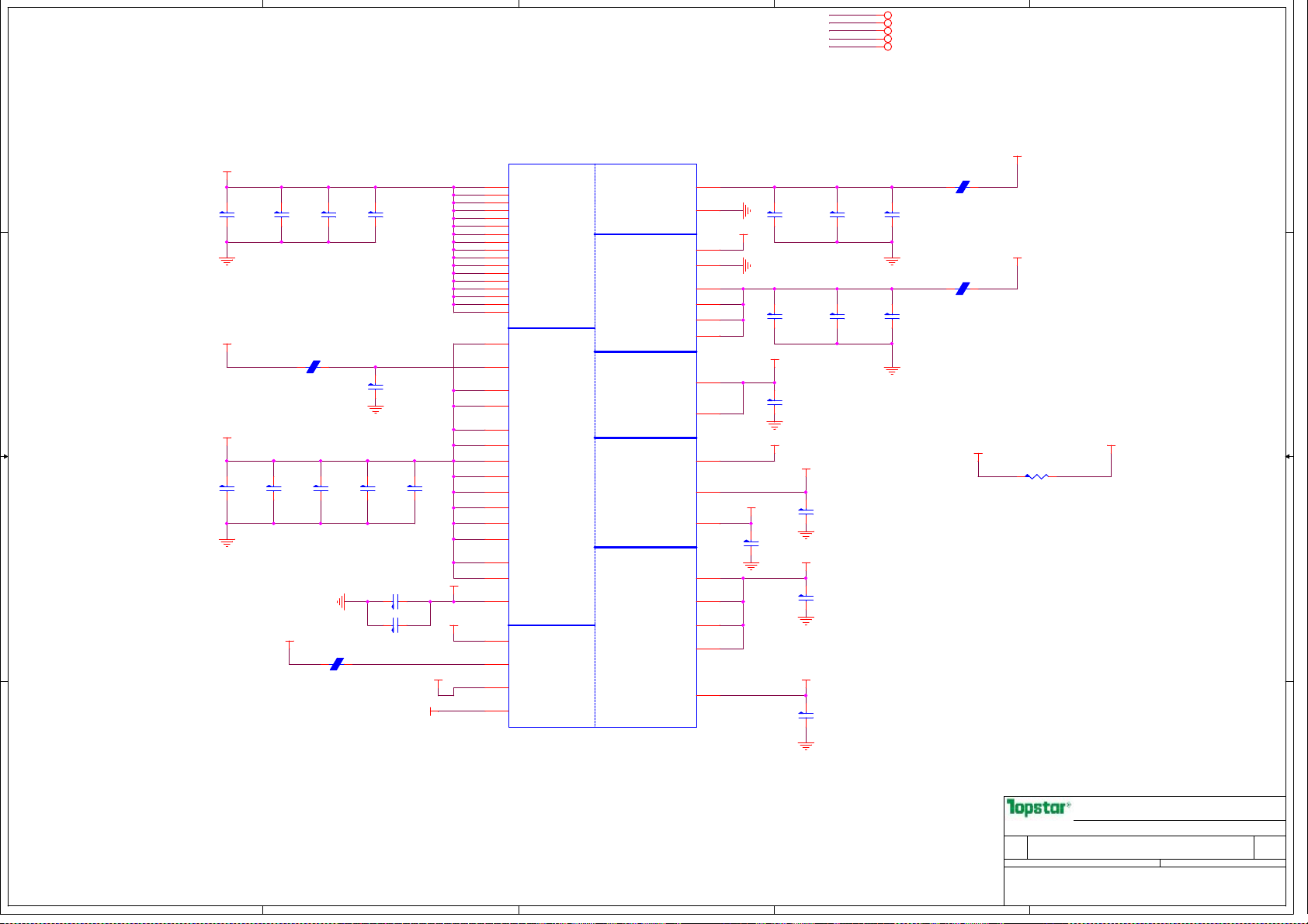
5
D D
4
3
2
+V1.8S 10,20,40,45
+V3.3S 7,14,15,16,17,18,19,20,22,24,25,29,30,31,32,33,34,35,40,41,42,43,44,45,47
+VCCVRM 22
+V1.5S 7,10,31,45
+V1.05S 6,7,9,15,16,17,22,30,41,44,47
1
FB0603
FB0603
+V3.3S
+V1.8S
167mA
R118 0
+V1.5S
R0603
POWER
VCC CORE
VCCIO
FDI
CRTLVDS
VCC TX_LVD S[1]
VCC TX_LVD S[2]
VCC TX_LVD S[3]
VCC TX_LVD S[4]
DMI
VCC DFTERM[1 ]
VCC DFTERM[2 ]
VCC DFTERM[3 ]
VCC DFTERM[4 ]
DFT / SPI HVCMOS
VCC ADAC
VSS ADAC
VCC ALVDS
VSS ALVDS
VCC 3_3[6]
VCC 3_3[7]
VCC VRM[3]
VCC DMI[1]
VCC CLKDMI
VCC SPI
U48
U47
AK3 6
AK3 7
AM37
AM38
AP3 6
AP3 7
V33
V34
AT1 6
AT2 0
AB3 6
AG1 6
AG1 7
AJ1 6
AJ1 7
V1
68mA1.7A
+V3.3S
1mA
70mA
40mA
47mA
+V1.05S
1uf/10V
10mA
+V3.3S
+VCCVRM
C78
C0402
2mA
VCCADAC
C34
C0402
0.01uF/16V,X7R
C69
C0402
0.01uF/16V,X7R
C38
0.1UF/10V,X7R
C0402
+V1.05S
1uf/10V
+V1.8S
0.1UF/10V,X7R
+V3.3S
1uf/10V
C50
C0402
C66
C0402
C63
C0402
C35
C0402C102
0.1UF/10V,X7R
VCCTX_LVDS
C67
C0402
0.01uF/16V,X7R
C25
C0805
10uf/6.3V
C71
C0805
10uf/6.3V
1 2
FB8
120ohm@100MHz,500mA
1 2
FB11
120ohm@100MHz,500mA
+VCCVRM
VCCVRM:Internal PLL and VRMs
1.5V for Mobile,1.8V for Desktop
AA2 3
AC2 3
AD2 1
AD2 3
AF2 1
AF2 3
AG2 1
AG2 3
AG2 4
AG2 6
AG2 7
AG2 9
AJ2 3
AJ2 6
AJ2 7
AJ2 9
AJ3 1
AN19
BJ2 2
AN16
AN17
AN21
AN26
AN27
AP2 1
AP2 3
AP2 4
AP2 6
AT2 4
AN33
AN34
BH29
AP1 6
BG6
AP1 7
AU20
U12G
VCC CORE[1]
VCC CORE[2]
VCC CORE[3]
VCC CORE[4]
VCC CORE[5]
VCC CORE[6]
VCC CORE[7]
VCC CORE[8]
VCC CORE[9]
VCC CORE[10 ]
VCC CORE[11 ]
VCC CORE[12 ]
VCC CORE[13 ]
VCC CORE[14 ]
VCC CORE[15 ]
VCC CORE[16 ]
VCC CORE[17 ]
VCC IO[28]
VCC APLLEX P
VCC IO[15]
VCC IO[16]
VCC IO[17]
VCC IO[18]
VCC IO[19]
VCC IO[20]
VCC IO[21]
VCC IO[22]
VCC IO[23]
VCC IO[24]
VCC IO[25]
VCC IO[26]
VCC 3_3[3]
VCC VRM[2]
Vcc AFDIPL L
VCC IO[27]
VCC DMI[2]
CPT_PPT_Rev_0p5
+V1.05S
10uf/6.3V
C0805
C C
+V1.05S
+V1.05S
C52
1uf/10V
C0402
FB16
120ohm@100MHz,500mA
1 2
ns
C55
1uf/10V
C0402
FB0603
C62
1uf/10V
C0402
VCCAPLL
C106
1uf/10V
C0402
ns
3.7A
C82
C0805
10uf/6.3V
B B
C46
C0402
1uf/10V
+V1.05S
C54
C0402
1uf/10V
1 2
120ohm@100MHz,500mA
FB12
ns
1uf/10V
FB0603
C48
C0402
C533
0.1UF/10V,X7R
C540
0.1UF/10V,X7R
C0402
C0402
+V1.05S
C39
C0402
1uf/10V
VCCFDIPLL
+V1.05S
+V3.3S
+VCCVRM
A A
Page Name
Page Name
Page Name
Size
Size
Size
Project Name Rev
Project Name Rev
Project Name Rev
A3
A3
A3
Date: Sheet of
Date: Sheet of
Date: Sheet of
PROPERTY NOTE: this document contains information confidential and property to
PROPERTY NOTE: this document contains information confidential and property to
PROPERTY NOTE: this document contains information confidential and property to
TOPSTAR and shall not be reproduced or transferred to other documents or disclosed
TOPSTAR and shall not be reproduced or transferred to other documents or disclosed
TOPSTAR and shall not be reproduced or transferred to other documents or disclosed
to others or used for any purpose other than that for which it was obtained without
to others or used for any purpose other than that for which it was obtained without
to others or used for any purpose other than that for which it was obtained without
the expressed written consent of TOPSTAR
the expressed written consent of TOPSTAR
the expressed written consent of TOPSTAR
5
4
3
2
TOPSTAR TECHNOLOGY
TOPSTAR TECHNOLOGY
TOPSTAR TECHNOLOGY
杨华明
(Sky Yang)
杨华明
(Sky Yang)
杨华明
(Sky Yang)
PCH PWR 1/2
PCH PWR 1/2
PCH PWR 1/2
CL42 EVT
CL42 EVT
CL42 EVT
1
A
A
21 51Wednesday, January 09, 2013
21 51Wednesday, January 09, 2013
21 51Wednesday, January 09, 2013
A
Page 22
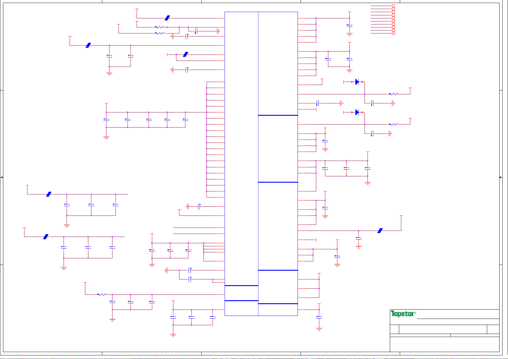
5
+V3.3SB
+V3.3S
D D
VerC: Add R113 tie to +V3.3SB support deep S3
Swain 111206
1 2
FB7
120ohm@100MHz,500mA
FB0603
+V1.05S
C44
C0805
10uf/6.3V
903mA
C97
C0805
10uf/6.3V
C C
+V1.05S
1 2
FB14
120ohm@100MHz,500mA
B B
A A
+V1.05S
FB15
1 2
120ohm@100MHz,500mA
5
FB0603
FB0603
C0805
C101
10uf/6.3V
C0805
C96
10uf/6.3V
CRB
上每路用 了一个
+V1.05S
C103
1uf/10V
80mA
C100
1uf/10V
C0402
R782 0
80mA
C0402
VCCADPLLA
220uF
VCCADPLLB
ns
R0402
4.7uf/10V
+V1.05S
+V3.3AL
1uf/10V
CRB have two pcs 22uF ,three pcs 1uF
C49
C0805
10uf/6.3V
C156
10uf/6.3V
ns
C0805
C155
10uf/6.3V
C0805
C321
C0805
0.1UF/10V,X7R
C31
C0402
C322
C0402
1mA
4
FB9
1 2
120ohm@100MHz,500mA
R1020R0402 noDS3
R1130R0402 DS3
+V1.05S
C57
C0402
1uf/10V
+V1.05S
1uf/10V
0.1UF/10V,X7R
4
C75
C0402
C481
C0402
C79
C0402
1uf/10V
+VCCVRM
1uf/10V
PCH_EC_RTC
FB0603 ns
C37 0.1UF/10V,X7R
C42
0.1UF/10V,X7R
ns
C0402
FB13
1 2
120ohm@100MHz,500mA
C74 0.1UF/10V,X7R
C0402
ns
C51
C0402
1uf/10V
VCCADPLLA
VCCADPLLB
C73
C0402
1uf/10V
C40
C45
1mA
C297
C0402
0.1UF/10V,X7R
VCCACLK
C0402
VCC_CLK33
FB0603 ns
C33
C0402
0.1UF/10V,X7R
C65
C0402
C0402
0.1UF/10V,X7R
C0402
0.1UF/10V,X7R
ns
C295
C0402
0.1UF/10V,X7R
55mA
95mA
0.1UF/10V,X7R
U12J
AD4 9
T16
V12
T38
BH23
AL2 9
AL2 4
AA1 9
AA2 1
AA2 4
AA2 6
AA2 7
AA2 9
AA3 1
AC2 6
AC2 7
AC2 9
AC3 1
AD2 9
AD3 1
W2 1
W2 3
W2 4
W2 6
W2 9
W3 1
W3 3
N16
Y49
BD4 7
BF4 7
AF1 7
AF3 3
AF3 4
AG3 4
AG3 3
V16
T17
V19
BJ8
A22
C298
C0402
CPT_PPT_Rev_0p5
VCC ACLK
VCC DSW3_ 3
DCP SUSBYP
VCC 3_3[5]
VCC APLLDMI 2
VCC IO[14]
DCP SUS[3]
VCC ASW[1]
VCC ASW[2]
VCC ASW[3]
VCC ASW[4]
VCC ASW[5]
VCC ASW[6]
VCC ASW[7]
VCC ASW[8]
VCC ASW[9]
VCC ASW[10 ]
VCC ASW[11 ]
VCC ASW[12 ]
VCC ASW[13 ]
VCC ASW[14 ]
VCC ASW[15 ]
VCC ASW[16 ]
VCC ASW[17 ]
VCC ASW[18 ]
VCC ASW[19 ]
VCC ASW[20 ]
DCP RTC
VCC VRM[4]
VCC ADPLLA
VCC ADPLLB
VCC IO[7]
VCC DIFFCL KN[1]
VCC DIFFCL KN[2]
VCC DIFFCL KN[3]
VCC SSC
DCP SST
DCP SUS[1]
DCP SUS[2]
V_P ROC_IO
VCC RTC
3
POWER
Clock and Miscellaneous
CPURTC
3
PCI/GPIO/LPCMISC
SATA USB
HDA
VCC IO[29]
VCC IO[30]
VCC IO[31]
VCC IO[32]
VCC IO[33]
VCC SUS3_3[7 ]
VCC SUS3_3[8 ]
VCC SUS3_3[9 ]
VCC SUS3_3[1 0]
VCC SUS3_3[6 ]
VCC IO[34]
V5R EF_SUS
DCP SUS[4]
VCC SUS3_3[1 ]
V5R EF
VCC SUS3_3[2 ]
VCC SUS3_3[3 ]
VCC SUS3_3[4 ]
VCC SUS3_3[5 ]
VCC 3_3[1]
VCC 3_3[8]
VCC 3_3[4]
VCC 3_3[2]
VCC IO[5]
VCC IO[12]
VCC IO[13]
VCC IO[6]
VCC APLLSA TA
VCC VRM[1]
VCC IO[2]
VCC IO[3]
VCC IO[4]
VCC ASW[22 ]
VCC ASW[23 ]
VCC ASW[21 ]
VCC SUSHDA
N26
P26
P28
T27
T29
T23
T24
V23
V24
P24
T26
M26
AN23
AN24
P34
N20
N22
P20
P22
AA1 6
W1 6
T34
AJ2
AF1 3
AH13
AH14
AF1 4
AK1
AF1 1
AC1 6
AC1 7
AD1 7
T21
V21
T19
P32
10mA
95mA
+V1.05S
1mA
C80
C0402 ns
1uf/10V
+V3.3AL
1mA
+V3.3AL
228mA
+V1.05S
VCCSATAPLL
+VCCVRM
+V1.05S
+V3.3AL
0.1UF/10V,X7R
C32
C0402
0.1UF/10V,X7R
C36
C0402
1uf/10V
C47
C0402
0.1UF/10V,X7R
C64
C0402
1uf/10V
C28
C0402
2
+V1.05S
+V3.3AL
C29
C0402
0.1UF/10V,X7R
+V3.3AL
+V1.05S
D12
SOD323
LRC LMDL914T1G 100V 200mA
D13
+V3.3S
SOD323
LRC LMDL914T1G 100V 200mA
C300
C0402
0.1UF/10V,X7R
C43
C0402
1uf/10V
2
C59
1uf/10V
C0402
1
1
+V3.3S
C56
C0805
10uf/6.3V
ns
C19
C0402
0.1UF/10V,X7R
C27
C0402
1uf/10V
C480
C0402
0.1UF/10V,X7R
FB10
1 2
ns
+V1.8S 10,20,21,40,45
+V3.3S 7,14,15,16,17,18,19,20,21,24,25,29,30,31,32,33,34,35,40,41,42,43,44,45,47
+VCCVRM 21
+V1.5S 7,10,21,31,45
+V1.05S 6,7,9,15,16,17,21,30,41,44,47
+V3.3AL 7,15,16,17,19,20,24,28,31,33,40,43,45
+V5AL_PCH 45
+V5S 15,16,24,25,27,28,29,30,40,42,44,45,47
PCH_EC_RTC 15,17
+V3.3SB 7,15,17,20,28,31,33,35,37,38,39,45
+V5AL_PCH
R50 10
R0402
+V5S
R21 10
R0402
+V1.05S
FB0603
120ohm@100MHz,500mA
Page Name
Page Name
Page Name
Size
Size
Size
Project Name Rev
Project Name Rev
Project Name Rev
A3
A3
A3
Date: Sheet of
Date: Sheet of
Date: Sheet of
PROPERTY NOTE: this document contains information confidential and property to
PROPERTY NOTE: this document contains information confidential and property to
PROPERTY NOTE: this document contains information confidential and property to
TOPSTAR and shall not be reproduced or transferred to other documents or disclosed
TOPSTAR and shall not be reproduced or transferred to other documents or disclosed
TOPSTAR and shall not be reproduced or transferred to other documents or disclosed
to others or used for any purpose other than that for which it was obtained without
to others or used for any purpose other than that for which it was obtained without
to others or used for any purpose other than that for which it was obtained without
the expressed written consent of TOPSTAR
the expressed written consent of TOPSTAR
the expressed written consent of TOPSTAR
1
TOPSTAR TECHNOLOGY
TOPSTAR TECHNOLOGY
TOPSTAR TECHNOLOGY
杨华明
(Sky Yang)
杨华明
(Sky Yang)
杨华明
(Sky Yang)
PCH PWR 2/2
PCH PWR 2/2
PCH PWR 2/2
CL42 EVT
CL42 EVT
CL42 EVT
1
22 51Wednesday, January 09, 2013
22 51Wednesday, January 09, 2013
22 51Wednesday, January 09, 2013
A
A
A
Page 23

5
U12H
H5
VSS [0]
AA1 7
VSS [1]
AA2
VSS [2]
AA3
VSS [3]
AA3 3
VSS [4]
D D
C C
B B
A A
AA3 4
AB1 1
AB1 4
AB3 9
AB4
AB4 3
AB5
AB7
AC1 9
AC2
AC2 1
AC2 4
AC3 3
AC3 4
AC4 8
AD1 0
AD1 1
AD1 2
AD1 3
AD1 9
AD2 4
AD2 6
AD2 7
AD3 3
AD3 4
AD3 6
AD3 7
AD3 8
AD3 9
AD4
AD4 0
AD4 2
AD4 3
AD4 5
AD4 6
AD8
AE2
AE3
AF1 0
AF1 2
AD1 4
AD1 6
AF1 6
AF1 9
AF2 4
AF2 6
AF2 7
AF2 9
AF3 1
AF3 8
AF4
AF4 2
AF4 6
AF5
AF7
AF8
AG1 9
AG2
AG3 1
AG4 8
AH11
AH3
AH36
AH39
AH40
AH42
AH46
AH7
AJ1 9
AJ2 1
AJ2 4
AJ3 3
AJ3 4
AK1 2
AK3
CPT_PPT_Rev_0p5
VSS [5]
VSS [6]
VSS [7]
VSS [8]
VSS [9]
VSS [10]
VSS [11]
VSS [12]
VSS [13]
VSS [14]
VSS [15]
VSS [16]
VSS [17]
VSS [18]
VSS [19]
VSS [20]
VSS [21]
VSS [22]
VSS [23]
VSS [24]
VSS [25]
VSS [26]
VSS [27]
VSS [28]
VSS [29]
VSS [30]
VSS [31]
VSS [32]
VSS [33]
VSS [34]
VSS [35]
VSS [36]
VSS [37]
VSS [38]
VSS [39]
VSS [40]
VSS [41]
VSS [42]
VSS [43]
VSS [44]
VSS [45]
VSS [46]
VSS [47]
VSS [48]
VSS [49]
VSS [50]
VSS [51]
VSS [52]
VSS [53]
VSS [54]
VSS [55]
VSS [56]
VSS [57]
VSS [58]
VSS [59]
VSS [60]
VSS [61]
VSS [62]
VSS [63]
VSS [64]
VSS [65]
VSS [66]
VSS [67]
VSS [68]
VSS [69]
VSS [70]
VSS [71]
VSS [72]
VSS [73]
VSS [74]
VSS [75]
VSS [76]
VSS [77]
VSS [78]
VSS [79]
5
VSS [80]
VSS [81]
VSS [82]
VSS [83]
VSS [84]
VSS [85]
VSS [86]
VSS [87]
VSS [88]
VSS [89]
VSS [90]
VSS [91]
VSS [92]
VSS [93]
VSS [94]
VSS [95]
VSS [96]
VSS [97]
VSS [98]
VSS [99]
VSS [100]
VSS [101]
VSS [102]
VSS [103]
VSS [104]
VSS [105]
VSS [106]
VSS [107]
VSS [108]
VSS [109]
VSS [110]
VSS [111]
VSS [112]
VSS [113]
VSS [114]
VSS [115]
VSS [116]
VSS [117]
VSS [118]
VSS [119]
VSS [120]
VSS [121]
VSS [122]
VSS [123]
VSS [124]
VSS [125]
VSS [126]
VSS [127]
VSS [128]
VSS [129]
VSS [130]
VSS [131]
VSS [132]
VSS [133]
VSS [134]
VSS [135]
VSS [136]
VSS [137]
VSS [138]
VSS [139]
VSS [140]
VSS [141]
VSS [142]
VSS [143]
VSS [144]
VSS [145]
VSS [146]
VSS [147]
VSS [148]
VSS [149]
VSS [150]
VSS [151]
VSS [152]
VSS [153]
VSS [154]
VSS [155]
VSS [156]
VSS [157]
VSS [158]
AK3 8
AK4
AK4 2
AK4 6
AK8
AL1 6
AL1 7
AL1 9
AL2
AL2 1
AL2 3
AL2 6
AL2 7
AL3 1
AL3 3
AL3 4
AL4 8
AM11
AM14
AM36
AM39
AM43
AM45
AM46
AM7
AN2
AN29
AN3
AN31
AP1 2
AP1 9
AP2 8
AP3 0
AP3 2
AP3 8
AP4
AP4 2
AP4 6
AP8
AR2
AR4 8
AT1 1
AT1 3
AT1 8
AT2 2
AT2 6
AT2 8
AT3 0
AT3 2
AT3 4
AT3 9
AT4 2
AT4 6
AT7
AU24
AU30
AV1 6
AV2 0
AV2 4
AV3 0
AV3 8
AV4
AV4 3
AV8
AW 14
AW 18
AW 2
AW 22
AW 26
AW 28
AW 32
AW 34
AW 36
AW 40
AW 48
AV1 1
AY12
AY22
AY28
4
4
AY4
AY42
AY46
AY8
B11
B15
B19
B23
B27
B31
B35
B39
F45
BB1 2
BB1 6
BB2 0
BB2 2
BB2 4
BB2 8
BB3 0
BB3 8
BB4
BB4 6
BC1 4
BC1 8
BC2
BC2 2
BC2 6
BC3 2
BC3 4
BC3 6
BC4 0
BC4 2
BC4 8
BD4 6
BD5
BE2 2
BE2 6
BE4 0
BF1 0
BF1 2
BF1 6
BF2 0
BF2 2
BF2 4
BF2 6
BF2 8
BD3
BF3 0
BF3 8
BF4 0
BF8
BG1 7
BG2 1
BG3 3
BG4 4
BG8
BH11
BH15
BH17
BH19
H10
BH27
BH31
BH33
BH35
BH39
BH43
BH7
D12
D16
D18
D22
D24
D26
D30
D32
D34
D38
D42
E18
E26
G18
G20
G26
G28
G36
G48
H12
H18
H22
H24
H26
H30
H32
H34
3
B7
D3
D8
F3
3
U12I
VSS [159]
VSS [160]
VSS [161]
VSS [162]
VSS [163]
VSS [164]
VSS [165]
VSS [166]
VSS [167]
VSS [168]
VSS [169]
VSS [170]
VSS [171]
VSS [172]
VSS [173]
VSS [174]
VSS [175]
VSS [176]
VSS [177]
VSS [178]
VSS [179]
VSS [180]
VSS [181]
VSS [182]
VSS [183]
VSS [184]
VSS [185]
VSS [186]
VSS [187]
VSS [188]
VSS [189]
VSS [190]
VSS [191]
VSS [192]
VSS [193]
VSS [194]
VSS [195]
VSS [196]
VSS [197]
VSS [198]
VSS [199]
VSS [200]
VSS [201]
VSS [202]
VSS [203]
VSS [204]
VSS [205]
VSS [206]
VSS [207]
VSS [208]
VSS [209]
VSS [210]
VSS [211]
VSS [212]
VSS [213]
VSS [214]
VSS [215]
VSS [216]
VSS [217]
VSS [218]
VSS [219]
VSS [220]
VSS [221]
VSS [222]
VSS [223]
VSS [224]
VSS [225]
VSS [226]
VSS [227]
VSS [228]
VSS [229]
VSS [230]
VSS [231]
VSS [232]
VSS [233]
VSS [234]
VSS [235]
VSS [236]
VSS [237]
VSS [238]
VSS [239]
VSS [240]
VSS [241]
VSS [242]
VSS [243]
VSS [244]
VSS [245]
VSS [246]
VSS [247]
VSS [248]
VSS [249]
VSS [250]
VSS [251]
VSS [252]
VSS [253]
VSS [254]
VSS [255]
VSS [256]
VSS [257]
VSS [258]
CPT_PPT_Rev_0p5
VSS [259]
VSS [260]
VSS [261]
VSS [262]
VSS [263]
VSS [264]
VSS [265]
VSS [266]
VSS [267]
VSS [268]
VSS [269]
VSS [270]
VSS [271]
VSS [272]
VSS [273]
VSS [274]
VSS [275]
VSS [276]
VSS [277]
VSS [278]
VSS [279]
VSS [280]
VSS [281]
VSS [282]
VSS [283]
VSS [284]
VSS [285]
VSS [286]
VSS [287]
VSS [288]
VSS [289]
VSS [290]
VSS [291]
VSS [292]
VSS [293]
VSS [294]
VSS [295]
VSS [296]
VSS [297]
VSS [298]
VSS [299]
VSS [300]
VSS [301]
VSS [302]
VSS [303]
VSS [304]
VSS [305]
VSS [306]
VSS [307]
VSS [308]
VSS [309]
VSS [310]
VSS [311]
VSS [312]
VSS [313]
VSS [314]
VSS [315]
VSS [316]
VSS [317]
VSS [318]
VSS [319]
VSS [320]
VSS [321]
VSS [322]
VSS [323]
VSS [324]
VSS [325]
VSS [328]
VSS [329]
VSS [330]
VSS [331]
VSS [333]
VSS [334]
VSS [335]
VSS [337]
VSS [338]
VSS [340]
VSS [342]
VSS [343]
VSS [344]
VSS [345]
VSS [346]
VSS [347]
VSS [348]
VSS [349]
VSS [350]
VSS [351]
VSS [352]
H46
K18
K26
K39
K46
K7
L18
L2
L20
L26
L28
L36
L48
M12
P16
M18
M22
M24
M30
M32
M34
M38
M4
M42
M46
M8
N18
P30
N47
P11
P18
T33
P40
P43
P47
P7
R2
R48
T12
T31
T37
T4
W3 4
T46
T47
T8
V11
V17
V26
V27
V29
V31
V36
V39
V43
V7
W1 7
W1 9
W2
W2 7
W4 8
Y12
Y38
Y4
Y42
Y46
Y8
BG2 9
N24
AJ3
AD4 7
B43
BE1 0
BG4 1
G14
H16
T36
BG2 2
BG2 4
C22
AP1 3
M14
AP3
AP1
BE1 6
BC1 6
BG2 8
BJ2 8
2
Page Name
Page Name
Page Name
Size
Size
Size
Project Name Rev
Project Name Rev
Project Name Rev
A3
A3
A3
Date: Sheet of
Date: Sheet of
Date: Sheet of
PROPERTY NOTE: this document contains information confidential and property to
PROPERTY NOTE: this document contains information confidential and property to
PROPERTY NOTE: this document contains information confidential and property to
TOPSTAR and shall not be reproduced or transferred to other documents or disclosed
TOPSTAR and shall not be reproduced or transferred to other documents or disclosed
TOPSTAR and shall not be reproduced or transferred to other documents or disclosed
to others or used for any purpose other than that for which it was obtained without
to others or used for any purpose other than that for which it was obtained without
to others or used for any purpose other than that for which it was obtained without
the expressed written consent of TOPSTAR
the expressed written consent of TOPSTAR
the expressed written consent of TOPSTAR
2
1
TOPSTAR TECHNOLOGY
TOPSTAR TECHNOLOGY
TOPSTAR TECHNOLOGY
杨华明
(Sky Yang)
杨华明
(Sky Yang)
杨华明
(Sky Yang)
PCH GND
PCH GND
PCH GND
CL42 EVT
CL42 EVT
CL42 EVT
1
A
A
23 51Wednesday, January 09, 2013
23 51Wednesday, January 09, 2013
23 51Wednesday, January 09, 2013
A
Page 24
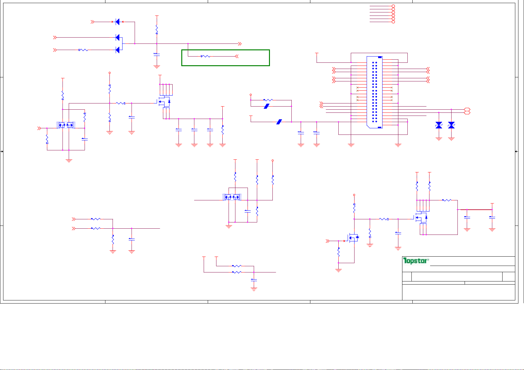
5
D2
LRC LMDL914T1G 100V 200mA
SOD323
+12V
1
2
R519
100K
R0402
R0402
R242
510K
R0402
1
ns
D3
LRC 30V 200mA 5ns
SOT23
200KR549
3
AON7410
SO8_26_130
LIDR#33
D D
C C
LVDS_BKLTEN18
HW_OFF_BKLT#33
+V3.3AL
R70
51K
R0402
Q4
SC70_6
L2N7002DW1T1G
LVDS_VDDEN18
2
R475
510K
R0402
1
1KR57 R0402
R56
3456
1K
R0402
0.01uF/25V,X7R
c0402
+V3.3S
R2
51K
R0402
Q2
4
C15
0.01uF/25V,X7R
C0402
4
C2
C0402
1000pF/50V,X7R
+V3.3S
56789
D
G
S
3
BKLT_ON
1KR76 R0402
BKLT_ON_EC 33
CL341 VerC: Add R76 to Pretect EC 2012/12/25
+12V
F2 1.5A T-Fuse
123
0.1UF/10V,X7R
C14
C0402
LCDVDD
10uf/6.3V
C20
C0805
C21
C0805
10uf/6.3V
nsC18
LCDVDD
R72
2.2K
R0402
ns
1 2
100ohm@100MHz,3A
+VDC
FB0805
R0603 ns
FB28
7V_LED_Panel(min)
FB27
1 2
300ohm@100MHz,2A
FB0805
6V_LED_Panel(min)
EDID_CLK18
EDID_DATA18
C1
C0603
0.1uF/25V,X7R
LCDVDD
LVDS_YAM018
LVDS_YAP018
LVDS_YAM218
LVDS_YAP218
LCDVDD
+5VAL_Camera
BKLT_PWM
INVT_VDD
C286
0.1uF/25V,X7R
C0603
2
LCDCON1
WAFER Econn
CNS40_LCD_R1
112
334
556
778
9910
111112
131314
151516
171718
191920
212122
232324
252526
272728
292930
31
31
33
33
35
35
37
37
39
39
+V3.3S 7,14,15,16,17,18,19,20,21,22,25,29,30,31,32,33,34,35,40,41,42,43,44,45,47
+VDC 37,39,40,41,44,47
+V3.3AL 7,15,16,17,19,20,22,28,31,33,40,43,45
+V5S 15,16,22,25,27,28,29,30,40,42,44,45,47
+V5AL 33,36,39,41,43,45,46,47
+12V 27,39,45,46
41
41
2
4
6
8
10
12
14
16
18
20
22
24
26
28
30
32
32
34
34
36
36
38
38
40
40
42
42
EDID PWR
BKLT_ON
EGA10603V05A1-B
ESDPAD_R0402
LVDS_YAM1 18
LVDS_YAP1 18
LVDS_CLKAP 18
LVDS_CLKAM 18
D21
12
ESDPAD_R0402
ns
1
D22
12
EGA10603V05A1-B
ns
CAM_USB_PN3 19
CAM_USB_PP3 19
LCDVDD +VDC
6V_LED_Panel(min)
R71
100
R0603
LVDS_VDDEN
+V3.3S +V3.3AL
Q3
SC70_6
2
L2N7002DW1T1G
3456
1
C23
C0402
100pF/50V,NPO
R5 0 R0603 ns
R7 0 R0603
B B
EC_BKLT_PWM33
LVDS_BKLTCTL18
A A
5
R4 100 R0402 ns
R735 100 R0402
R3
10K
R0402
BKLT_PWM
C3
C0402
100pF/50V,NPO
4
R98
100K
R0402
R92
100K
R0402
EDID PWR
C4
C0402
0.1UF/10V,X7R
3
+12V
R115
100K
R0402
7V_LED_Panel(min)
Camera
Stuff KBC controlled camera power.
TU142 VerC.
Camera_ON#33
1
CAM_SW
R362
100K
R0402
+12V
R357
100K
R0402
CAM_SW
3
Q27
2
L2N7002LT1G
SOT23
CAM_SW
+V5AL +V5S
R353
R354
0
0
R0805
R0805
ns
R356 0 R0805
Q26
AON7410
SO8_26_130
100KR355
R0402
CAM_SW
R245
510K
R0402
CAM_SW
2
56789
D
CAM_SW
4
G
S
C536
0.01uF/25V,X7R
C0402
CAM_SW
Page Name
Page Name
Page Name
Size
Size
Size
Project Name Rev
Project Name Rev
Project Name Rev
Custom
Custom
Custom
Date: Sheet of
Date: Sheet of
Date: Sheet of
PROPERTY NOTE: this document contains information confidential and property to
PROPERTY NOTE: this document contains information confidential and property to
PROPERTY NOTE: this document contains information confidential and property to
TOPSTAR and shall not be reproduced or transferred to other documents or disclosed
TOPSTAR and shall not be reproduced or transferred to other documents or disclosed
TOPSTAR and shall not be reproduced or transferred to other documents or disclosed
to others or used for any purpose other than that for which it was obtained without
to others or used for any purpose other than that for which it was obtained without
to others or used for any purpose other than that for which it was obtained without
the expressed written consent of TOPSTAR
the expressed written consent of TOPSTAR
the expressed written consent of TOPSTAR
NO_CAM_SW
500mA
123
TOPSTAR TECHNOLOGY
TOPSTAR TECHNOLOGY
TOPSTAR TECHNOLOGY
Robin
Robin
Robin
LVDS&Inverter CONN
LVDS&Inverter CONN
LVDS&Inverter CONN
TU142 PVT
TU142 PVT
TU142 PVT
1
C288
0.1uF/10V,X7R
C0402
24 51Sunday, April 07, 2013
24 51Sunday, April 07, 2013
24 51Sunday, April 07, 2013
+5VAL_Camera
C287
10uf/6.3V
C0805
C
C
C
Page 25
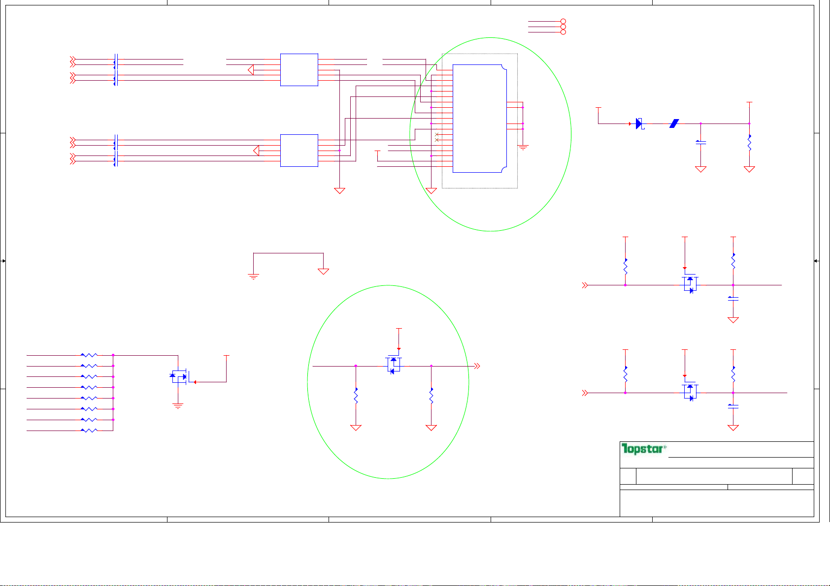
5
IN_D2-18
D D
IN_D2+18
IN_D0+18
IN_D0-18
MCH_CLK_D4-18
MCH_CLK_D4+18
IN_D1-18
IN_D1+18
C371 0.1uF/10V,X7R
C370 0.1uF/10V,X7R
C364 0.1uF/10V,X7R
C365 0.1uF/10V,X7R
C367 0.1uF/10V,X7R
C366 0.1uF/10V,X7R
C373 0.1uF/10V,X7R
C372 0.1uF/10V,X7R
IFPC_TXD2N
IFPC_TXD2P
IFPC_TXD0P
IFPC_TXD0N
IFPC_TXC#
IFPC_TXC
IFPC_TXD1N
IFPC_TXD1P
IFPC_TXD2P
IFPC_TXD2N
GND_HDMI
GND_HDMI
4
GU4
1
D1+
2
D1-
3
GND1
4
D2+
D2-5NC1
TVU1240R1A
SON10_0D5_1
GU3
1
D1+
2
D1-
3
GND1
4
D2+
D2-5NC1
TVU1240R1A
SON10_0D5_1
NC4
NC3
GND2
NC2
NC4
NC3
GND2
NC2
10
9
8
7
6
10
9
8
7
6
IFPC_TXD2P
IFPC_TXD2N
IFPC_TXD0P
IFPC_TXD0N
+V5_HDMI
IFPC_TXD1P
IFPC_TXD1N
IFPC_TXC
IFPC_TXC#
3
IFPC_TXD2N
IFPC_TXD2P
5VDDCCK_HDMI
5VDDCDA_HDMI
HDMIHP_C
HDMI_CON1
1
D2+
2
D2 SHTELD
3
D2-
4
D1+
5
D1 SHTELD
6
D1-
7
D0+
8
D0 SHTELD
9
D0-
10
CK+
11
CK SHTELD
12
CK-
13
CEC
14
RESERVED
15
SCL
16
SDA
17
DCC/CEC_G ND
18
+5V
19
HP_DET
hdmi_d_1b
GND1
GND2
GND3
GND4
20
21
22
23
GND_HDMI
2
+V5S 15,16,22,24,27,28,29,30,40,42,44,45,47
+V3.3S 7,14,15,16,17,18,19,20,21,22,24,29,30,31,32,33,34,35,40,41,42,43,44,45,47
+V3.3AL 7,15,16,17,19,20,22,24,28,31,33,40,43,45
+V5S
SOD123
FB29
1 2
FB0603
120ohm@100MHz,500mA
D23
1
1N5819W DIODESEMI
1
+V5_HDMI
C158
0.1UF/10V,X7R
C0402
GND_HDMIGND_HDMI
R219
100K
R0402
C C
GND_HDMIGND_HDMI
F42 VerB: Changed HDMI_CON1 to the same with C03 20110820
06/08:HDMI CONN on MB-Zhouzm
+V3.3S +V3.3S
GR23
2.2K
GND_HDMI
B B
+V5S
GM_HDMI_DDC_CLK18
1
IFPC_TXD2N
IFPC_TXD2P
IFPC_TXD1N
IFPC_TXD1P
IFPC_TXD0N
IFPC_TXD0P
IFPC_TXC#
IFPC_TXC
A A
R289 680 R0402
R292 680 R0402
R288 680 R0402
R287 680 R0402
R274 680 R0402
R275 680 R0402
R272 680 R0402
R273 680 R0402
5
Q17
LBSS138LT1G
sot23
3
2
+V3.3S
1
重点注意
4
Layout
HDMIHP_C
走线!!!
GR12
100K
R0402
3
L2N7002LT1G
SOT23
GQ2
2
R806
1M
R0402
3
MCH_HDMI_HPD 18
GM_HDMI_DDC_DATA18
2
R0402
+V3.3S +V3.3S
GR24
2.2K
R0402
Page Name
Page Name
Page Name
Size
Size
Size
Project Name Rev
Project Name Rev
Project Name Rev
B
B
B
Date: Sheet of
Date: Sheet of
Date: Sheet of
PROPERTY NOTE: this document contains information confidential and property to
PROPERTY NOTE: this document contains information confidential and property to
PROPERTY NOTE: this document contains information confidential and property to
TOPSTAR and shall not be reproduced or transferred to other documents or disclosed
TOPSTAR and shall not be reproduced or transferred to other documents or disclosed
TOPSTAR and shall not be reproduced or transferred to other documents or disclosed
to others or used for any purpose other than that for which it was obtained without
to others or used for any purpose other than that for which it was obtained without
to others or used for any purpose other than that for which it was obtained without
the expressed written consent of TOPSTAR
the expressed written consent of TOPSTAR
the expressed written consent of TOPSTAR
1
2
1
2
+V5_HDMI
Q40
3
LBSS138LT1G
sot23
+V5_HDMI
Q41
3
LBSS138LT1G
sot23
TOPSTAR TECHNOLOGY
TOPSTAR TECHNOLOGY
TOPSTAR TECHNOLOGY
Robin
Robin
Robin
HDMI CONN
HDMI CONN
HDMI CONN
TU142 PVT
TU142 PVT
TU142 PVT
R250
4.7K
R0402
5VDDCCK_HDMI
C172
C0402
10pF/50V,NPO
GND_HDMI
R231
4.7K
R0402
C162
C0402
10pF/50V,NPO
GND_HDMIGND_HDMI GND_HDMI
1
5VDDCDA_HDMI
25 51Wednesday, January 09, 2013
25 51Wednesday, January 09, 2013
25 51Wednesday, January 09, 2013
C
C
C
Page 26

5
4
3
2
1
D D
C C
B B
TOPSTAR TECHNOLOGY
TOPSTAR TECHNOLOGY
TOPSTAR TECHNOLOGY
Robin
Robin
Robin
Page Name
Page Name
Page Name
Size
Size
Size
Project Name Rev
Project Name Rev
A A
Project Name Rev
A
A
A
Date: Sheet of
Date: Sheet of
Date: Sheet of
PROPERT Y NOTE: this document contains information confidential and property to
PROPERT Y NOTE: this document contains information confidential and property to
PROPERT Y NOTE: this document contains information confidential and property to
TOPSTAR and shall not be reproduced or transferred to other documents or disclosed
TOPSTAR and shall not be reproduced or transferred to other documents or disclosed
TOPSTAR and shall not be reproduced or transferred to other documents or disclosed
to others or used for any purpose other than that for which it was obtained without
to others or used for any purpose other than that for which it was obtained without
to others or used for any purpose other than that for which it was obtained without
the expressed written consent of TOPSTAR
the expressed written consent of TOPSTAR
the expressed written consent of TOPSTAR
HDMI DB CONN
HDMI DB CONN
HDMI DB CONN
TU142 PVT
TU142 PVT
TU142 PVT
C
C
C
26 51Wednesday, January 09, 2013
26 51Wednesday, January 09, 2013
26 51Wednesday, January 09, 2013
Page 27
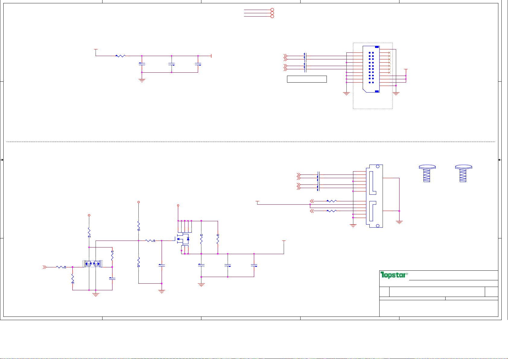
5
4
3
+V5S 15,16,22,24,25,28,29,30,40,42,44,45,47
EC_RTC 15,39,45
+12V 24,39,45,46
2
1
SATA HDD Conn
D D
C C
B B
Zero Power ODD
SC70_6
L2N7002DW1T1G
Zero Power ODD
SATA_ODD_PWRGT20
A A
R464
1K
R0402
Zero Power ODD
5
+V5S
EC_RTC
R469
51K
R0402
Q29
2
1
R467
510K
R0402
Zero Power ODD
Average 1A,Peak 1.5A
FB24 0 R0805
C11
C0805
4.7uf/10V
SATA ODD Conn
+12V
R471
200K
R0402
Zero Power ODD
R472
R470
3456
1K
R0402
Zero Power ODD1MR474
PC203
0.01uF/25V,X7R
c0402
ns
200K
R0402
Zero Power ODD
R0402
Zero Power ODD
PQ50
AON7410
SO8_26_130
Zero Power ODD
4
PC196
0.01uF/25V,X7R
C0402
Zero Power ODD
4
C246
0.1UF/10V,X7R
C0402
+V5S
56789
D
G
S
123
C245
0.1UF/10V,X7R
C0402
R466
0
R0805
Normal ODD
C9
C0805
4.7uf/10V
V_HDD
R468
0
R0805
Normal ODD
Average 1A,Peak 1.5A
C537
0.1UF/10V,X7R
C0402
3
SATA_TXP015
SATA_TXN015
SATA_RXN015
SATA_RXP015
V_ODD
C538
0.1UF/10V,X7R
C0402
C487 0.01uF/16V,X7R C0402
C486 0.01uF/16V,X7R C0402
C399 0.01uF/16V,X7R C0402
C400 0.01uF/16V,X7R C0402
Close to connector as possible
the same distance to connector
SATA_TXP515
SATA_TXN515
SATA_RXN515
SATA_RXP515
SATA_ODD_PRSNT#20
SATA_ODD_DA#19,33
V_ODD
TU142 VerB: Changed SATA_HDD1 to 20pin
Wafer CONN 620901000004 2011-12-20
C485 0.01uF/16V,X7R C0402
C484 0.01uF/16V,X7R C0402
C335 0.01uF/16V,X7R C0402
C331 0.01uF/16V,X7R C0402
Zero power ODD
R137 0
R0402
R465 0 R0402
2
SATA_HDD1
WAFER Econn
CNS2X10_1_R
S1
S2
S3
S4
S5
S6
S7
P1
P2
P3
P4
P5
P6
21
21
2
112
4
334
6
556
8
778
10
9910
12
111112
14
131314
16
151516
18
171718
20
191920
22
22
SATA_CON1
GND1
A+
A-
GND6
GND2
BB+
GND3
DP
+5V_1
+5V_2
MD
GND7
GND4
GND5
JFS SATA ODD
SATAODD_D_50A
Page Name
Page Name
Page Name
Size
Size
Size
B
B
B
Date: Sheet of
Date: Sheet of
Date: Sheet of
PROPERTY NOTE: this document contains information confidential and property to
PROPERTY NOTE: this document contains information confidential and property to
PROPERTY NOTE: this document contains information confidential and property to
TOPSTAR and shall not be reproduced or transferred to other documents or disclosed
TOPSTAR and shall not be reproduced or transferred to other documents or disclosed
TOPSTAR and shall not be reproduced or transferred to other documents or disclosed
to others or used for any purpose other than that for which it was obtained without
to others or used for any purpose other than that for which it was obtained without
to others or used for any purpose other than that for which it was obtained without
the expressed written consent of TOPSTAR
the expressed written consent of TOPSTAR
the expressed written consent of TOPSTAR
V_HDD
SATAODD_B1
14
Screw 2*5mm
ASSY
15
D_BOT
TOPSTAR TECHNOLOGY
TOPSTAR TECHNOLOGY
TOPSTAR TECHNOLOGY
Robin
Robin
Robin
SATA HDD&ODD
SATA HDD&ODD
SATA HDD&ODD
Project Name Rev
Project Name Rev
Project Name Rev
TU142 PVT
TU142 PVT
TU142 PVT
1
SATAODD_B2
Screw 2*5mm
ASSY
27 51Wednesday, January 09, 2013
27 51Wednesday, January 09, 2013
27 51Wednesday, January 09, 2013
C
C
C
Page 28

5
DCCBBAA
Touch Pad Conn
4
3
+V5S 15,16,22,24,25,27,29,30,40,42,44,45,47
+V3.3AL 7,15,16,17,19,20,22,24,31,33,40,43,45
+V3.3SB 7,15,17,20,22,31,33,35,37,38,39,45
2
1
D
TPCLK33
TPDAT33
1
2
7
3
7
4
8
5
8
6
TP_CON1
CNS6_0D5_RA1
FPC Cotex
1
2
3
4
5
6
TPCLK
TPDAT
+V5S
+V5S
TPDAT
TPCLK
+V5S
R133
10K
R0402
C53
22pF/50V,NPO
C0402
R132
10K
R0402
+V5S
C107
C0402
0.1UF/10V,X7R
C109
1uf/10V
C0402
+V3.3AL
Power Button
IOPR2改为1M,IOPR4改为10K,
解决电池电压低时无法开机问题
PSW1
334
112
T1.5
BUTTON4_S
4
PWRSWVCC1
2
PC350
1000pF/50V,X7R
C0402
PWR_SW_VCC2
PR416 10K R0402
PR417 30K
PC351
1000pF/50V,X7R
C0402
1
R543
1M
R0402
R0402
+V3.3SB
R580
10K
R0402
3
Q31
2
L2N7002LT1G
SOT23
HV_Isense_SYSP 37
C379
C0402
1000pF/50V,X7R
PWR_SW_VCC2
12
PESD1
ESDPAD_R0402
EGA1-0603-V05
PWRSW# 33
PWR_SW_VCC2 39
R135
47K
R0402
ns
TPDAT
TPCLK
Install R134,R135 for KB used
Swain 100812
5
4
R134
47K
R0402
ns
C108
C0402
0.1UF/10V,X7R
TOPSTAR TECHNOLOGY
TOPSTAR TECHNOLOGY
TOPSTAR TECHNOLOGY
Robin
Robin
Page Name
Page Name
Page Name
Size
Size
Size
Project Name Rev
Project Name Rev
Project Name Rev
Custom
Custom
Custom
Date: Sheet of
Date: Sheet of
Date: Sheet of
PROPERTY NOTE: this document contains information confidential and property to
PROPERTY NOTE: this document contains information confidential and property to
PROPERTY NOTE: this document contains information confidential and property to
TOPSTAR and shall not be reproduced or transferred to other documents or disclosed
TOPSTAR and shall not be reproduced or transferred to other documents or disclosed
TOPSTAR and shall not be reproduced or transferred to other documents or disclosed
to others or used for any purpose other than that for which it was obtained without
to others or used for any purpose other than that for which it was obtained without
to others or used for any purpose other than that for which it was obtained without
the expressed written consent of TOPSTAR
the expressed written consent of TOPSTAR
the expressed written consent of TOPSTAR
3
2
Robin
TP CONN&PWRSW
TP CONN&PWRSW
TP CONN&PWRSW
TU142 PVT
TU142 PVT
TU142 PVT
C
C
C
28 51Wednesday, January 09, 2013
28 51Wednesday, January 09, 2013
28 51Wednesday, January 09, 2013
1
Page 29

5
In order to prevent the built-in LDO damaged from
D D
+V5S
C C
PD# of Codec pull up rails change from +V5S to +V3.3S.
TU142 VerC.
R2760
SHUTDOWN#
AZALIA_CODEC_RST#
<<Attention>>
For power_on/off de-pop circuit and system booting warning signal:
Please System BIOS Engineer Note :
1. If you want the system make warning signal after power on , please
B B
A A
let EC_MUTE# High.
2. If your design want to system make warning signal(for explame CPU
or Memory haven't been plugged in), please remove Q2 transistor.
AMP_SHDW3 3
R0402
D33
SOD323
1
LRC LMDL914 T1G 100V 2 00mA
1
D35
LRC LMDL914 T1G 100V 2 00mA
SOD323
5
over-voltage on +5VD or Standby power line. Use
the line suppressing device.
ANALOGDIGITAL
FB34
FB0805
300ohm@10 0MHz,2A
12
D36
SOD523
TVN S523
C522
C0805
10uf/6.3 V
MOAT
300ohm@10 0MHz,2A
300ohm@10 0MHz,2A
FB0805
ns
Q25
1
L2N7002LT 1G
SOT23
FB35
3
2
FB0805
FB33
+V3.3S
R976
1K
R0402
R309
10K
R0402
For VB5 and VB6
3
Q24
L2N7002LT 1G
SOT23
2
PVDD1
C517
C0805
10uf/6.3 V
PVDD2
C529
C0805
10uf/6.3 V
GND_AUD GND_AUD
1
AVDD
0.1uF/1 0V,X7R
GND_AUD
0.1uF/1 0V,X7R
C530
C0402
0.1uF/1 0V,X7R
C523
C0402
C442
C0402
AMP_SHDW
48mA
GND_AUD
Place next to pin 39
AZALIA_CODEC_SDOUT1 5
AZALIA_CODEC_BITCLK1 5
AZALIA_SDATAIN015
AZALIA_CODEC_SYNC15
AZALIA_CODEC_RST#15
SURR_OUT_RSURR_OUT_L
Q23
1
L2N7002LT 1G
SOT23
4
R342 75 R0402
R627 75 R0402
GND_AUD
C520
C0603
2.2uf/10 V
C521
C0603
2.2uf/10 V
30
31
32
33
34
35
36
G4
GND
G5
CBP
CBN
GND
G6
GND
37
AVSS2
38
EAPD
AVDD2
39
PVDD1
40
SPK-L+
41
SPK-L-
42
PVSS1
43
PVSS2
44
SPK-R-
45
SPK-R+
46
PVDD2
47
EAPD
48
SPDIFO
G7
ICTP
GND
G8
GND
G9
GND
Spilt by DGND
+INTSPL
-INTSPL
-INTSPR MIC2-R
+INTSPR
T82ns
+V3.3S
CPVEE
HP-OUT-L
HP-OUT-R
MIC1-VREFO-L
ALC269Q-VB6-CG
DVDD11GPIO0/DMIC-DATA2GPIO1/DMIC-CL K3PD#4SDATA-OUT5BIT-CLK6DVSS27SDATA-IN8DVDD-IO9SYNC10RESET#11PCBEEP
50mA
PD#
A_GPIO1
C440
C0402
A_GPIO0
T8
T2
ns
ns
R326 33
R0402
C532 22pF /50V,NPO
C0402
R341
10K
R0402
ICTP
ICTP
AZALIA_CODEC_BITCLK
+V5S
R625
10K
R0402
3
1
2
Q21
L2N7002LT 1G
SOT23
C441
C0805
10uf/6.3 V
0.1uF/1 0V,X7R
If HD_RESET high level is 1.5V(The signal level of HDA_Link are 1.5V) ,
please moidfy gate voltage of Q2 transistor to 1.5V; and use BSS138
or 2SK3018 transistor
3
3
Q22
1
L2N7002LT 1G
SOT23
2
2
AMP_SHDW3 3
4
SURR_OUT_R
SURR_OUT_L
MIC1-VREFO_R MIC2_R EF
MIC1-VREFO-L
MIC2-VREFO
GND_AUD
C524
C0805
28
29
LDO-CAP
MIC2-VREFO
MIC1-VREFO-R
R2630
R0402
R301 4.7K R0 402
C515
C0603
2.2uf/10 V
10uf/6.3 V
AVDD
U7
25
26
27
VREF
AVSS1
AVDD1
LINE1-R
LINE1-L
MIC1-R
MIC1-L
MONO-OUT
JDREF
Sense-B
MIC2-R
MIC2-L
LINE2-R
LINE2-L
Sense A
GND
GND
GND
QFNS48_0D4_ 1G
12
DIGITAL
(Include Thermal pad)
C263
C0402
100pF/5 0V,NPO
C531
C0805
10uf/6.3 V
SHUTDOWN#
R626
100K
R0402
ns
0.1uF/1 0V,X7R
GND_AUD
GND_AUD
24
23
22
21
20
19
18
17
16
15
14
13
G1
G2
G3
+V3.3S
C516
C0402
10uf/6.3 V
3
Place next to pin 27
C526
C525
C0402
C0805
0.1uF/1 0V,X7R
4.7uf/10 V
C0805
C0805
4.7uf/10 V
R0402
C527 C0805
4.7uf/10 V
C528 C0805
4.7uf/10 V
R306 39.2K, 1%
R376 20K,1%
EXT_MIC_L
GND_AUD
R0402
R0402
C272
C269
R478 20K,1%
MIC2-L
Sense_A HP_SENSE
ANALOG
C262
C0402
1uf/10V
C264
C0402
1uf/10V
R321
4.7K
R0402
C518
0.1uF/1 0V,X7R
C0402
-INTSPR
INTSPKR1
Wafer Econ n
CNS2_R
TU142 VerB: Sep erated Speaker CONN from 4PIN to 2PIN 2011- 12-20
R461 0 R0402 ns
R804 0 R0402
R805 0 R0402
FB19
nsFB0805
300ohm@10 0MHz,2A
C519
C0402
0.1uF/1 0V,X7R
ns
3
INT_MIC_L
MIC_SENSE
R329 51K
R0402
R322 75K
R0402
R324
4.7K
R0402
1
2
GND_AUD
2
+V5S 15,1 6,22,24,25 ,27,28,30,4 0,42,44,45 ,47
+V3.3S 7,14 ,15,16,17,1 8,19,20,21 ,22,24,25,3 0,31,32,33 ,34,35,40, 41,42,43,44 ,45,47
HP_COMBO
FB39 12 0ohm@100MHz,500mA
FB0603
HP_COMBO
1
MIC2_REF
R1019 100
C386
R1020
4.7uf/10 V
2.2K
ns
C0805
R0402
FB38
300ohm@10 0MHz,2A
GND_AUD
EXT_MIC_L_1
BTL_BEEP 33
SPKR 15
3
3
1
2
4
4
SURR_OUT_L
SURR_OUT_R
+INTSPL+INTSPR
-INTSPL
INTSPKL1
Wafer
CNS2_V
MIC2-VREFO
INT_MIC_L
TU142 VerB: Add a MIC_CON1 on motherboard fo r B cover
MIC and reserve d a MB positio n 2011-12-20
FB0805
300ohm@10 0MHz,2A
FB37
C390
C0402
100pF/50V,N PO
GND_AUD GND_AUD GND_AUD
FB0805
300ohm@10 0MHz,2A
FB0805
300ohm@10 0MHz,2A
100pF/5 0V,NPO
TU142 VerB: Cha nged Audio Com bo jack to i-ph one
type and modify peripheral ci rcuit for jack detect
2011-12-20
3
1
3
1
2
2
4
4
GNDGND
R486 4. 7K
R0402
R347 1K
R0402
ns
C0402
FB36
FB32
C378
GND_AUD
2
R0402
FB0805
FB0805
D16
ESDPAD_R0402
EGA1-0603 -V05
ns
2 3
Q32
LMBT3904L T1G
SOT23
C384
C0402
100pF/50V,N PO
R6
1K
100pF/5 0V,NPO
R0402
FB21
12
ns
GND_AUD
R1022 1K
R1023
22k
R0402
R8
C382
1K
C0402
R0402
GND_AUD
300ohm@10 0MHz,2A
12
C181
100pF/5 0V,NPO
C0402
R1017
1K
R0402
ns
R1021
100K
R0402
ns
R0402
EGA1-0603 -V05
ESDPAD_R0402
EXT_MIC_L_1
EGA1-0603 -V05
ESDPAD_R0402
EXT_MIC_L
GND_AUD
+V5S+V5U_AU
EXT_MIC_L_1
R1018 22k
Audio COMBO Jack
GND_AUD
12
D31
ns
D34
ns
1 2
1 2
GND_AUD
+
1
2
MIC1
Microphone
BZ_D6027
ASSY
i-Phone type
R0402_Sh ort
0R383
ns
D37
EGA1-0603 -V05
ESDPAD_R0402
ns
Page Name
Page Name
Page Name
Size
Size
Size
Project Name Rev
Project Name Rev
Project Name Rev
Custom
Custom
Custom
Date: Sheet of
Date: Sheet of
Date: Sheet of
PROPERTY NOTE: th is document con tains informatio n confidentia l and prop erty to
PROPERTY NOTE: th is document con tains informatio n confidentia l and prop erty to
PROPERTY NOTE: th is document con tains informatio n confidentia l and prop erty to
TOPSTAR an d shall not b e reprodu ced or tran sferred to other docu ments or disclos ed
TOPSTAR an d shall not b e reprodu ced or tran sferred to other docu ments or disclos ed
TOPSTAR an d shall not b e reprodu ced or tran sferred to other docu ments or disclos ed
to other s or used fo r any purp ose other t han that fo r which it was obtaine d without
to other s or used fo r any purp ose other t han that fo r which it was obtaine d without
to other s or used fo r any purp ose other t han that fo r which it was obtaine d without
the expresse d written conse nt of TOPSTAR
the expresse d written conse nt of TOPSTAR
the expresse d written conse nt of TOPSTAR
1
R2790
R0402
R1015
200K
R0402
GND_AUD GND_AUD
LBSS138LT 1G
R0402
C383
10uf/6.3 V
C0805
GND_AUD
Audio6_s2
Audio Jack
2
Mic
5
Left
7
Det
6
Res
4
Right
3
Gnd
HP_MIC_OUT1
GND_AUD
HP_COMBO
R1016 22k R 0402
AZALIA(ALC269)
AZALIA(ALC269)
AZALIA(ALC269)
1
HP_SENSE
Q30
3
L2N7002LT 1G
SOT23
1
2
MIC_SENSE
3
Q28
sot23
1
2
HP_SENSE
+V5U_AU
TOPSTAR T ECHNOLOGY
TOPSTAR T ECHNOLOGY
TOPSTAR T ECHNOLOGY
Robin
Robin
Robin
TU142 PVT
TU142 PVT
TU142 PVT
C
C
29 51Wedne sday, January 0 9, 2013
29 51Wedne sday, January 0 9, 2013
29 51Wedne sday, January 0 9, 2013
C
Page 30

5
4
Over temperture Protect Circuit
3
2
+V5S 15,16,22,24,25,27,28,29,40,42,44,45,47
+V3.3S 7,14,15,16,17,18,19,20,21,22,24,25,29,31,32,33,34,35,40,41,42,43,44,45,47
+V1.05S 6,7,9,15,16,17,21,22,41,44,47
1
D D
+V1.05S
R330
10K
C C
R0402
SHDN_LOCK# 43
3456
THERMTRIP#7,20
R332 10K
R0402
R333
100K
R0402
C266
1000pF/50V,X7R
C0402
2
1
Q19
LMBT3904DW1T1G
SC70_6
3
Q20
2
L2N7002LT1G
SOT23
ALT_ON33
Use for temperature alarm driver.
B B
1
R331
100K
R0402
FAN Controller Circuit
+V5S
+V3.3S
C290
2.2uf/10V
C0603
R81 200K
R0402
C291
0.1UF/10V,X7R
C0402
+V3.3S
Vfan
1
LRC LMDL914T1G 100V 200mA
R82
4.7K
R0402
FAN1_V 33
D14
SOD323
C26
10uf/6.3V
C0805
8
EN/FON#
GND
7
GND
6
GND
5
GND
U9
P2793AB0/1.6*VSET 500mA
SO8_50_150
Throttling/
Un-throttling
Shut-Down
VIN
VOUT
VSET
4.7uf/10V
1
2
3
4
C0805
C22
R361
10K
ns
R0402
1
2
3
CPUFAN1
1
4
2
3
5
WAFER
CNS3_V
+V3.3S
4
5
R404
10K
R0402
FAN_BACK 33
High-5V
CPU
THRMTRIP#
THERM_ALERT#
Thermal
sensor
A A
5
AND
SHDN#
VIN
VDC
Shut Down
Throttling on
Throttling Off
CPU Temperature
0
85
100
90
95
4
(Degree)
Middle-4V
Low-3V
3
FAN1_V=3.30V,Vfan=5V
FAN1_V=2.65V,Vfan=4V
FAN1_V=1.98V,Vfan=3V
65
55
90 10050 9570 75
85
8060
TOPSTAR TECHNOLOGY
TOPSTAR TECHNOLOGY
TOPSTAR TECHNOLOGY
Robin
Robin
Page Name
Page Name
Page Name
Size
Size
Size
Project Name Rev
Project Name Rev
Project Name Rev
B
B
B
Date: Sheet of
Date: Sheet of
Date: Sheet of
PROPERTY NOTE: this document contains information confidential and property to
PROPERTY NOTE: this document contains information confidential and property to
PROPERTY NOTE: this document contains information confidential and property to
TOPSTAR and shall not be reproduced or transferred to other documents or disclosed
TOPSTAR and shall not be reproduced or transferred to other documents or disclosed
TOPSTAR and shall not be reproduced or transferred to other documents or disclosed
to others or used for any purpose other than that for which it was obtained without
to others or used for any purpose other than that for which it was obtained without
to others or used for any purpose other than that for which it was obtained without
the expressed written consent of TOPSTAR
the expressed written consent of TOPSTAR
the expressed written consent of TOPSTAR
2
Robin
FAN/OTP
FAN/OTP
FAN/OTP
TU142 PVT
TU142 PVT
TU142 PVT
C
C
30 51Wednesday, January 09, 2013
30 51Wednesday, January 09, 2013
30 51Wednesday, January 09, 2013
1
C
Page 31

5
+DATA4
-DATA4
12
D D
D28
ESDPAD_R0402
EGA1-0603-V05
ns
12
D27
ESDPAD_R0402
EGA1-0603-V05
ns
Keep USB2.0 Signal stub short
90Ω/100MHz 0.5A
CHK12
MINICARD_USB_PN119
MINICARD_USB_PP119
C C
CLK_PCIE_MINICARD#16
CLK_PCIE_MINICARD16
PCIE_TXN4_WLAN16
PCIE_TXP4_WLAN16
PCIE_RXN4_WLAN16
PCIE_RXP4_WLAN16
BUF_PLT_RST#7,19,33,34
PCI_CLK_DEBUG19
+V3.3LAN
LPC_FRAME#15,33
B B
LPC_AD015,33
LPC_AD115,33
LPC_AD215,33
LPC_AD315,33
43
12
ICTPns
R792 0 DebugR0402
R793 0 R0402
R794 0 DebugR0402
R1024 0 R0603
R795 0 R0402
R796 0 DebugR0402
R797 0 R0402 Debug
R798 0 R0402 Debug
R800 0 R0402 Debug
R799 0 DebugR0402
BT_OFF#
R736 0 R0402
L4_0805_SHORT
ns
T50
-DATA4
+DATA4
PCIE_39
36
38
11
13
31
33
23
25
17
19
37
39
41
43
45
47
49
51
4
+V3.3LAN +V3.3LAN
R323
0
R0603
+V3.3S_PCIE
MPCIE1
MINIPCIE_HALF_L6
USB_DUSB_D+
REFCLKREFCLK+
PETN0
PETP0
PERN0
PERP0
RESERVED0
RESERVED1
RESERVED_P CIE0
RESERVED_P CIE1
RESERVED_P CIE2
RESERVED_P CIE3
RESERVED_P CIE4
RESERVED_P CIE5
RESERVED_P CIE6
RESERVED_P CIE7
R328
0
R0603
+V3.3AL_PCIE
52
2
+3.3V1
+3.3V0
3
+V1.5S
500mA
48
24
+3.3VAUX
28
6
+1.5V0
+1.5V1
+1.5V2
PERST#
WAKE#
46
44
42
22
1
minicard_Wake#
7
minicard_CLKREQ#_R
32
30
+V3.3LAN
5
R685 0 R0402
3
20
16
14
12
10
8
LED_W PAN#
LED_W LAN#
LED_W WAN#
CLKREQ#
SMB_DATA
SMB_CLK
CHANNEL_CLK
CHANNEL_DATA
RESERVED_DI SABLE
RESERVED_S IM0
RESERVED_S IM1
RESERVED_S IM2
RESERVED_S IM3
RESERVED_S IM4
PCIE mini Card
ns
ns
T52
ns ICTP
+V3.3LAN
T49
ICTP
T47
ICTP
R610 0 R0402
R616 0 nsR0402
R601 0 nsR0402
R600 0 nsR0402
R684 10K R0402
R605 0 R0402
0R1025
R0805
0R1026
R0805 ns
R607 0 R0402
ns
R606 0 R0402
BT_OFF# 33
2
+V3.3AL 7,15,16,17,19,20,22,24,28,33,40,43,45
+V1.5S 7,10,21,45
+V3.3SB 7,15,17,20,22,28,33,35,37,38,39,45
+V3.3S 7,14,15,16,17,18,19,20,21,22,24,25,29,30,32,33,34,35,40,41,42,43,44,45,47
+V3.3LAN 34
+V3.3AL
+V3.3LAN
+V3.3S
+V3.3SB
R611
10K
R617
R0402
10K
ns
R0402
ns
minicard_Wake#
minicard_CLKREQ#_R
WIRELESS_LED# 35
CL_RST1# 16
BUF_PLT_RST# 7,19,33,34
PCIE_WAKE# 17,20,34
minicard_CLKREQ# 16
CL_DATA1 16
CL_CLK1 16
+V3.3LAN
R604
10K
R0402
+V3.3S_PCIE
C252
10uf/6.3V
C0805
HW_RATIO_OFF# 33
C254
0.1UF/10V,X7R
C0402
+V3.3AL_PCIE
C261
10uf/6.3V
C0805
MPCIE_HALF_NUT1
D_BOT
Mylar_MPCIE1
Mylar_MPCIE
ASSY
C255
0.1UF/10V,X7R
C0402
1
PVC
C256
0.1UF/10V,X7R
C0402
WIFI Option和Debug Option
不可以同时上
A A
5
PCIE MINI CARD
GND0
GND1
GND2
GND5
GND4
GND3
9
4
4
15
21
35
29
27
GND11
GND10
GND9
GND8
GND7
GND6
18
40
34
26
GND1253GND1354GND1456GND1557GND1658GND1759GND1860GND1961GND20
50
55
3
+V1.5S
2
C251
10uf/6.3V
C0805
ns
C250
0.1UF/10V,X7R
C0402
Page Name
Page Name
Page Name
Size
Size
Size
Project Name Rev
Project Name Rev
Project Name Rev
B
B
B
Date: Sheet of
Date: Sheet of
Date: Sheet of
PROPERTY NOTE: this document contains information confidential and property to
PROPERTY NOTE: this document contains information confidential and property to
PROPERTY NOTE: this document contains information confidential and property to
TOPSTAR and shall not be reproduced or transferred to other documents or disclosed
TOPSTAR and shall not be reproduced or transferred to other documents or disclosed
TOPSTAR and shall not be reproduced or transferred to other documents or disclosed
to others or used for any purpose other than that for which it was obtained without
to others or used for any purpose other than that for which it was obtained without
to others or used for any purpose other than that for which it was obtained without
the expressed written consent of TOPSTAR
the expressed written consent of TOPSTAR
the expressed written consent of TOPSTAR
C249
0.1UF/10V,X7R
C0402
C253
0.1UF/10V,X7R
C0402
TOPSTAR TECHNOLOGY
TOPSTAR TECHNOLOGY
TOPSTAR TECHNOLOGY
Robin
Robin
Robin
PCIE MINI SLO
PCIE MINI SLO
PCIE MINI SLO
TU142 PVT
TU142 PVT
TU142 PVT
1
31 51Wednesday, January 09, 2013
31 51Wednesday, January 09, 2013
31 51Wednesday, January 09, 2013
C
C
C
Page 32
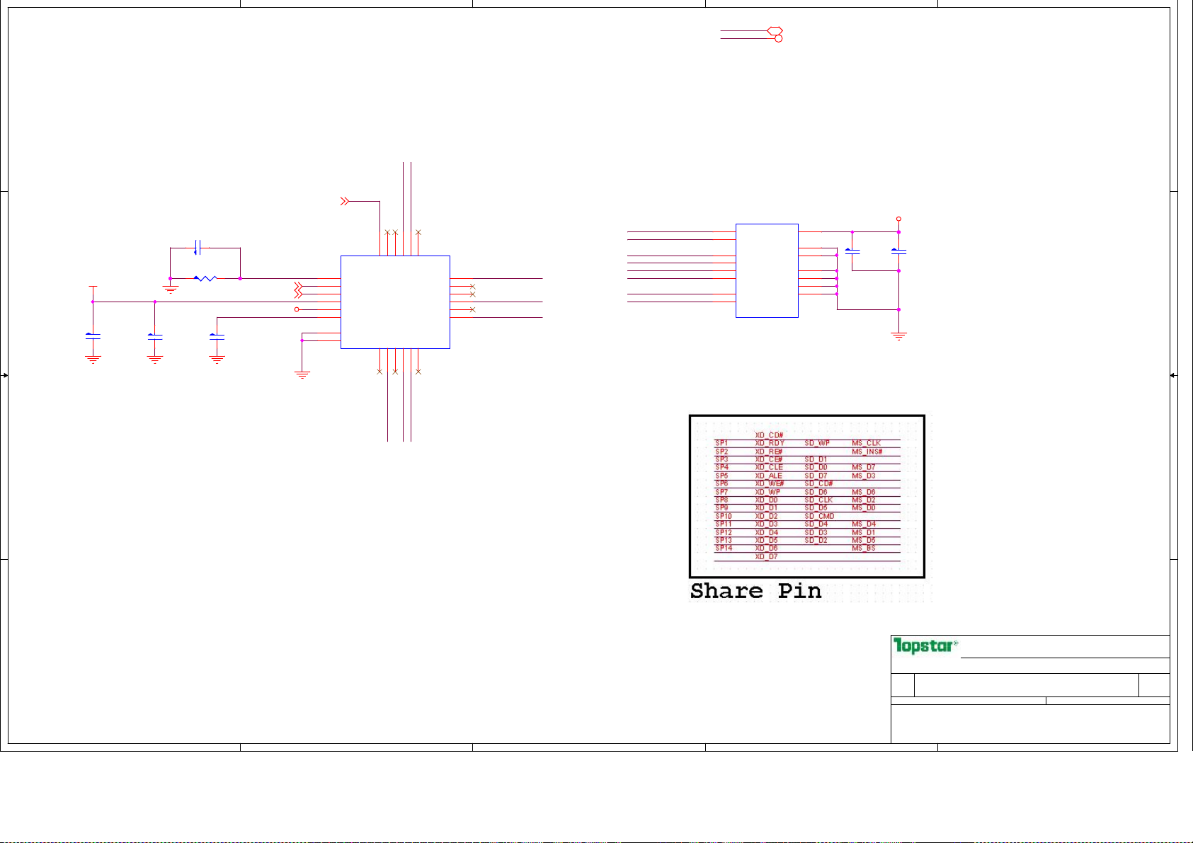
5
D D
4
3
2
+V3.3S 7,14,15,16,17,18,19,20,21,22,24,25,29,30,31,33,34,35,40,41,42,43,44,45,47
+V3.3AL 7,15,16,17,19,20,22,24,28,31,33,40,43,45
1
2IN1 CONN
CLK_CR_48M16
SD_D2_MS_D5
SD_D3_MS_D1
C388
C0402ns
100pF/50V,NPO
1
PWR_SW2
RREF
2
3
4
5
6
G1
G2
C389
C0402
R120
6.2k,1%
R0402
C394
C0402
1uf/10V
USB_CR_PN819
USB_CR_PP819
VREG
C C
+V3.3S
4.7uf/10V
C391
C0805
0.1UF/10V,X7R
U28
RREF
DM
DP
3V3_IN
CARD_3V3
V18
GND
GND
24
22
23
SP1119SP1220SP1321SP14
XD_D7
CLK_IN
RTS5138-GR
QFNS24_0D5_0D9G
QFN24
SP10
GPIO0
XD_CD#7SP18SP29SP310SP411SP5
SP9
SP8
SP7
SP6
18
17
16
15
14
13
SD_CMD
SD_CLK_MS_D2
SD_CD#
SD_CD#
SD_CMD
SD_D0_MS_D7
SD_D1
SD_D2_MS_D5
SD_D3_MS_D1
SD_CLK_MS_D2
SD_WP_MS_CLK
12
J2
10
CD
2
CMD
7
DAT0
8
DAT1
9
DAT2
1
CD/DAT3
5
CLK
11
SD_W P
2in1 Cardreader Black
SD_MMC
621001500002
VDD
VSS1
VSS2
4
3
6
12
G1
13
G2
14
G3
15
G4
PWR_SW2
C259
0.1uF/10V,X7R
C0402
C260
1uf/10V
C0402
IC Bottom Ground
SD_D1
SD_D0_MS_D7
SD_WP_MS_CLK
B B
TOPSTAR TECHNOLOGY
TOPSTAR TECHNOLOGY
TOPSTAR TECHNOLOGY
Robin
Robin
A A
5
4
3
2
Page Name
Page Name
Page Name
Size
Size
Size
Project Name Rev
Project Name Rev
Project Name Rev
B
B
B
Date: Sheet of
Date: Sheet of
Date: Sheet of
PROPERTY NOTE: this document contains information confidential and property to
PROPERTY NOTE: this document contains information confidential and property to
PROPERTY NOTE: this document contains information confidential and property to
TOPSTAR and shall not be reproduced or transferred to other documents or disclosed
TOPSTAR and shall not be reproduced or transferred to other documents or disclosed
TOPSTAR and shall not be reproduced or transferred to other documents or disclosed
to others or used for any purpose other than that for which it was obtained without
to others or used for any purpose other than that for which it was obtained without
to others or used for any purpose other than that for which it was obtained without
the expressed written consent of TOPSTAR
the expressed written consent of TOPSTAR
the expressed written consent of TOPSTAR
Robin
Cardreader(RTS5138)
Cardreader(RTS5138)
Cardreader(RTS5138)
TU142 PVT
TU142 PVT
TU142 PVT
1
C
C
32 51Wednesday, January 09, 2013
32 51Wednesday, January 09, 2013
32 51Wednesday, January 09, 2013
C
Page 33
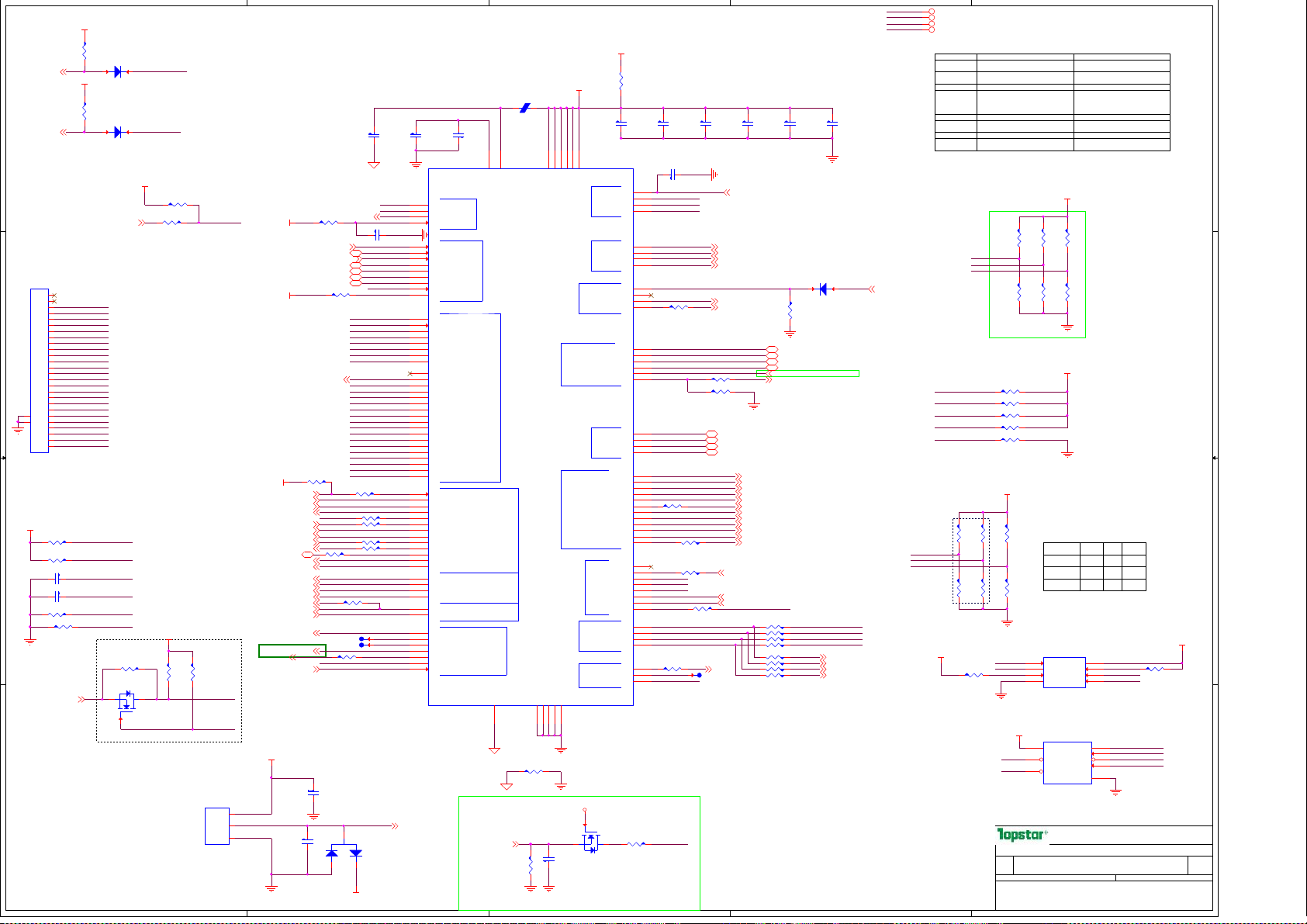
5
+V3.3S
R277
10K
R0402
D17
A20GATE
H_A20GATE20
D D
H_RCIN#2 0
KBCON1
FPC
CNS26_1_R_2D 5
26
26
25
25
24
24
23
23
22
22
21
21
20
20
19
19
18
18
C C
B B
A A
17
17
16
16
15
15
14
14
13
13
12
12
11
11
10
10
9
9
8
8
7
7
6
28
6
28
5
27
5
27
4
4
3
3
2
2
1
1
EC_V3.3AL
R577 10K
R0402
R313 10K ns
R0402
C195
C0402
100pF/5 0V,NPO
C381
C0402
100pF/5 0V,NPO
R658 1K R040 2
R123 100K R0 402
KB9010
PCH_SLP_S4#17
F42 VerB: Add SLP_S4# isolate circuit
for Deep S3 20110825
+V3.3S
R271
10K
R0402
SCANOUT15
SCANOUT10
SCANOUT11
SCANOUT14
SCANOUT13
SCANOUT12
SCANOUT3
SCANOUT6
SCANOUT8
SCANOUT7
SCANOUT4
SCANOUT2
SCANIN7
SCANOUT1
SCANOUT5
SCANIN4
SCANIN5
SCANOUT0
SCANIN2
SCANIN3
SCANOUT9
SCANIN1
SCANIN0
SCANIN6
BUF_PLT_RST#7,19,31,34
PM_SLP_S3#
PM_SLP_S4#
1
LRC LMDL914 T1G 100V 2 00mA
SOD323
D15
1
LRC LMDL914 T1G 100V 2 00mA
SOD323
LIDR#
ALT_ON
IMVP_ON
EC_OWNER_R
2
RCIN#
EC_V3.3AL
R572 4.7K R0402
ns
R5730
R0402
VerC: update GPIO07 to PCH_DPWROK output
Swain 111206
EC_V3.3AL
R314
R5830
10K
ns
R0402
3
Q18
L2N7002LT 1G
ns
1
SOT23
5
EC_PCI_RST#
R337
10K
ns
R0402
PM_SLP_S4#
EC_CTRL_S4
U37
APX9132A
SOT23_A
VS+
Output
GND
EC_V3.3AL
EC_V3.3AL
+V3.3AL
EC_OWNER15
CL341 VerC: Add SATA_ODD_DA# signal
to control ODD ejection 2012/12/25
1
2
3
与
3926
Pin109与Pin114
Pin103
作为比较后的输出
Pin100/101增加FANFB2/3
Pin74增加PECI
Pin83/84/85/86
Pin16
增加配置为
R602 47K R0402
CLK_EC_PCI19
INT_SERIRQ15
LPC_FRAME#1 5,31
R603 4.7K R0402
AC_IN_PCH17
ns
R570 1K
PM_SUS_STAT#17
PCH_DPWROK17
AC_IN37
PM_RSMRST#1 7,43
PWRSW#28
PM_SLP_S3#1 7,43
PM_SLP_S4#3 9,45
V1.05S_PWG41,43
IMVP_ON44
R574 0 R040 2 KB3930
H_PECI_EC7
ALT_ON30
V1_5_ON40
ALWAYS_ON39,45,46
MAIN_ON45
V1_05S_ON41
V0_75S_ON40
ICH_IMVP_PWRGD17
IMVP_PWRGD4 4
MAIN_PWROK7,17,43
EC_PROCHOT#7
SATA_ODD_DA#19, 27
+V3.3SB
ALW_PWROK39
C514
1000pF /50V,X7R
C0402
R476 0 R040 2KB9010
PC348
0.1UF/10V,X7R
C0402
不同点
增加电压输入功能
的功能
输入功能
增加配置为
OWM
的功能
EC_RUNTIME_SCI#20
C387 0.0 1uF/16V,X7R
LPC_AD015,31
LPC_AD115,31
LPC_AD215,31
LPC_AD315,31
SCANIN7
SCANIN6
SCANIN5
SCANIN4
SCANIN3
SCANIN2
SCANIN1
SCANIN0
SCANOUT15
SCANOUT14
SCANOUT13
SCANOUT12
SCANOUT11
SCANOUT10
SCANOUT9
SCANOUT8
SCANOUT7
SCANOUT6
SCANOUT5
SCANOUT4
SCANOUT3
SCANOUT2
SCANOUT1
SCANOUT0
LIDR#
R578 1K R040 2
R581 1K R040 2
PM_SLP_S3#
PM_SLP_S4#
R598 1.5 K,1%R0402
IMVP_ON
R582 2.2 K R0 402
ALT_ON
R473 0
R0402
T89ns
EC_CTRL_S4
LIDR#
D32
LBAT54SLT 1G
sot23
132
+V3.3SB
4
SMBUS2/3
的功能
V18R
C211
C243
C0402
C0402
0.1UF/10V,X7R
0.1UF/10V,X7R
1
A20GATE
GA20/GPIO0 0
2
RCIN#
KBRST#/GPIO01
20
SCI#/GPIO0E
37
C0402
EC_PCI_RST#
CLKREQ
R5710 ns
H_PECI_EC1
EC_OWNER_R
4
ECRST#
12
PCICLK
3
SERIRQ
4
LFRAME#
10
LAD0
8
LAD1
7
LAD2
5
LAD3
13
PCIRST#/GPIO05
38
CLKRUN#/GPIO 1D
62
KSI7/GPIO37
61
KSI6/GPIO36
60
KSI5/GPIO35
59
KSI4/GPIO34
58
KSI3/GPIO33
57
KSI2/GPIO32
56
KSI1/GPIO31
55
KSI0/GPIO30 /E51_TXD(ISP)
82
KSO17/GPIO4 9
81
KSO16/GPIO4 8
54
KSO15/GPIO2 F/E51_RXD(ISP)
53
KSO14/GPIO2 E
52
KSO13/GPIO2 D
51
KSO12/GPIO2 C
50
KSO11/GPIO2 B
49
KSO10/GPIO2 A
48
KSO9/GPIO29
47
KSO8/GPIO28
46
KSO7/GPIO27
45
KSO6/GPIO26
44
KSO5/GPIO25
43
KSO4/GPIO24
42
KSO3/GPIO23 /TP_ISP
41
KSO2/GPIO22 /TP_ANA_TEST
40
KSO1/GPIO21 /TP_PLL
39
KSO0/GPIO20 /TP_TEST
6
GPIO04
14
GPIO07/i_c lk_8051
15
GPIO08/i_c lk_peri
16
GPIO0A/CIR_ RX2/OWM
17
GPIO0B/ESB_CLK
18
GPIO0C/ESB_DAT_O /ESB_DAT_I
19
GPIO0D
32
GPIO18
36
GPIO1A/NUMLED#
73
GPIO40/CIR _RX
74
GPIO41/CIR _RLC_TX/PECI
89
GPIO50
127
GPIO59/TEST_CLKSPIC LKI
68
GPO3C
70
GPO3D
71
GPO3E
72
GPO3F
76
GPI43
75
GPI42
90
E51CS#/GPIO 52
30
E51TXD/GPIO16
31
E51RXD/GPIO1 7/E51CLK
92
E51TMR0/GPIO54 /WDT_LED#
93
E51INT0/GPIO 55/SCROLED#
91
E51TMR1/GPIO53 /CAPSLED#
95
E51INT1/GPIO 56
The 0ohm RES will across the isolate
island of anolog GND and digital GND
LIDR# 24
C210
C0402
1uf/10V
FB22
120ohm@10 0MHz,500mA
1 2
FB0603
124
67
V18R
AVCC
MSIC
LPC
KB
8051
AGND
69
R3190R0603
SUSCLK17
R565
100K
R0402
EC_V3.3AL
33
22
9
111
125
VCC
VCC
VCC
VCC
VCC96VCC
ADC PWM
FAN
FANPWM0/GPIO12
FANPWM1/GPIO13
PSCLK1/GPIO4 A/SCL2
PSDAT1/GPIO4B/SDA2
PSCLK2/GPIO4 C/SCL3
PS2
PSDAT2/GPIO4D/SDA3
SMBUS
KB3930
GPXIOA00/SDICS#
GPXIOA01/SDICL K
GPXIOA
GPXIOA02/SDIMOSI
GPXIOA03/FANFAB2
GPXIOA04/FANFB3
GPXIOA06/VCO UT
GPXIOD0/SDIMISO/ VCIN0
GPXIOD
GPIO
SPI
change to DG
By Johan 071224
CLK
XCLK32K/GPIO 57
GND
GND35GND24GND
GND
11
94
113
+V5AL
1
2
C376
C0402
18pF/50 V,NPO
3
+V3.3SB
U27
AD0/GPI38
AD1/GPI39
AD2/GPI3A
AD3/GPI3B
PWM0/GPIO0F
PWM1/GPIO10
PWM2/GPIO11
PWM3/GPIO19
FANFB0/GPIO14
FANFB1/GPIO15
PSCLK3/GPIO4 E
PSDAT3/GPIO4F
SDA1/GPIO47
SCL1//GPIO4 6
SDA0/GPIO45
SCL0/GPIO4 4
GPXIOA05
GPXIOA07
GPXIOA08
GPXIOA09
GPXIOA10
GPXIOA11
GPXIOD1
GPXIOD2
GPXIOD3/VCIN1
GPXIOD4
GPXIOD5
GPXIOD6
GPXIOD7
MISO
MOSI
SPICLK/GPIO58
SPICS#
XCLKI
XCLKO
KB3930
3
Q44
LBSS138LT 1G
sot23
3
1 2
10uf/6.3 V
R296
0
R0805
C206
C0805
C225
C244
C0402
C0402
0.1UF/10V,X7R
C385
C0402
3300pF /50V,X7R
SYS_I_Sense
EC_Code0
EC_Code1
EC_Code2
BTL_BEEP 29
POWERLED# 35
BT_OFF # 31
EC_BKLT_PWM 24
FAN1_V 30
Camera_ON# 24
R0402
PM_STATE
R311 0nsR0402
R305 10K R0402
SML1DATA 16
SML1CLK 16
SM_BAT_SDA2 38
SM_BAT_SCL2 3 8
AMP_SHDW
EC_ME_LOCK#
CHG_ON
R0402
R339 0 R040 2
R308 0 R040 2
R575 0 R040 2 KB9010
R5550 R336 0 R040 2 KB901 0
VCCSA_ON 42
T83
ns
63
64
65
66
21
23
25
34
28
29
26
27
83
84
85
86
87
88
80
79
78
77
97
98
99
100
101
102
103
104
105
106
107
108
109
110
112
114
115
116
117
118
119
120
126
128
121
122
123
R5640R0402
0.1UF/10V,X7R
R585 1K
SM_BAT_SDA2
SM_BAT_SCL2
R299 0
PCB_Mark0
PCB_Mark1
PCB_Mark2
GPXIOD7
EC_SPI_MISO_R
EC_SPI_MOSI_R
EC_SPI_SCK_R
EC_SPI_CS#_R
EC_32XCLK1
EC_32XCLK0
EC_32XCLK0
C223
C0402
0.1UF/10V,X7R
SYS_I_Sense 3 7
EXTSMI# 20
HW_RATIO_OFF# 31
CHG_LED# 35
BTL_LED# 35
PM_PWRBTN# 17
AMP_SHDW 29
EC_ME_LOCK# 15
CHG_ON 37
PCH_PWROK 17
EC_DRAMRST_CNTRL_ PCH 7
HW_OFF_BKLT # 24
AC_OFF 37
SUSACK# 17
ALW_ACK 1 7
BATT_IN# 38
BKLT_ON_EC 24
H_PECI_EC
R327 0 R040 2 KB393 0
R320 0 R040 2 KB393 0
R348 0 R040 2 KB393 0T86ns
R325 0 R040 2 KB393 0
R340 0 R040 2 KB901 0
R335 0 R040 2 KB901 0
R338 0 R040 2 KB901 0
C212
C232
C0402
0.1UF/10V,X7R
Vin>=1.5V turn on the cup FAN.
TPCLK 2 8
TPDAT 28
SM_CHG_SCL2 3 7
SM_CHG_SDA2 37
PM_SLP_SUS# 17,39,4 5
C0402
0.1UF/10V,X7R
D26
1
SOD323
LRC LMDL914 T1G 100V 2 00mA
R586
100K
R0402
EC_SPI_MISO
EC_SPI_MOSI
SPI_SCK
SPI_CS#
PCH_SPI_MISO_Q 15
PCH_SPI_MOSI_Q 15
PCH_SPI_CLK_Q 15
PCH_SPI_CS0#_Q 15
2
FAN_BACK 30
+V3.3S 7 ,14,15,16,1 7,18,19,20 ,21,22,24,2 5,29,30,31 ,32,34,35,4 0,41,42,43 ,44,45,47
+V3.3SB 7,15,1 7,20,22,28 ,31,35,37,3 8,39,45
+V3.3AL 7, 15,16,17,1 9,20,22,24 ,28,31,40,4 3,45
+V5AL 2 4,36,39,41 ,43,45,46, 47
GPIO function
AD function 6 PCS AD 8PCS AD
PECI function at Pin74 at Pin118
HW Voltage
comparator
GWG function Pin108 supportNo support
SPI function No Internal flash Internal flash 128KB
Pin127 Have TEST_CLKSPICLK1 No TEST_CLKSPICLK1
PWR fail No support Pin32 POWER_FAIL1
SM_BAT_SDA2
SM_BAT_SCL2
AMP_SHDW
EC_ME_LOCK#
CHG_ON
Pin68&70&71&72 Only GPO All GPIO
Pin63&64&65&66&75&76 Only GPI
Pin109 VCIN0
Pin114 VCIN1
PIn103 VCOUT
R738
R0402
EC_Code0
EC_Code1
EC_Code2
EC Code:
F41 00 0
F42 00 1
TU142 01 0
TU151 01 1
SU341 10 0
TU131 10 1
CL42 11 0
R783
R0402
R315 2.2K R0402
R317 2.2K R0402
R719 10K nsR0402
R300 10 K
EC_V3.3AL
CL341 Ve rC: Cha nge PCB mark to VerC 20 12/12/2 5
R556
R561
10K
10K
R0402
R0402
EC_V3.3AL
ns
R553
R560
10K
10K
R0402
R0402
ns
SPI_CS#
EC_SPI_MISO
R540 4.7 K
R0402
Page Name
Page Name
Page Name
Size
Size
Size
C
C
C
Date: Sheet of
Date: Sheet of
Date: Sheet of
PROPERTY NOTE: th is document con tains informatio n confidentia l and prop erty to
PROPERTY NOTE: th is document con tains informatio n confidentia l and prop erty to
PROPERTY NOTE: th is document con tains informatio n confidentia l and prop erty to
TOPSTAR an d shall not b e reprodu ced or tran sferred to other docu ments or disclos ed
TOPSTAR an d shall not b e reprodu ced or tran sferred to other docu ments or disclos ed
TOPSTAR an d shall not b e reprodu ced or tran sferred to other docu ments or disclos ed
to other s or used fo r any purp ose other t han that fo r which it was obtaine d without
to other s or used fo r any purp ose other t han that fo r which it was obtaine d without
to other s or used fo r any purp ose other t han that fo r which it was obtaine d without
the expresse d written conse nt of TOPSTAR
the expresse d written conse nt of TOPSTAR
the expresse d written conse nt of TOPSTAR
PCB_Mark0
PCB_Mark1
PCB_Mark2
2
1
KB3930 KB9010
新增
Pin73 AD6 & Pin74 AD7
Pin109 VCIN0
Pin102 VCIN1
PIn103 VCOUT1
Pin104 VCOUT0
Pin128&119&120 Add GPIO function
Pin100 POWER_FAIL0
EC_V3.3AL
R737
R739
10K
10K
10K
R0402
R0402
ns
R784
R785
10K
10K
WP#1
EC_V3.3AL
WP#1
HOLD#1
10K
R0402
R0402
ns
ns
EC_V3.3AL
10KR562 nsR0402
R558
10K
R0402
ns
Fuction P.M2 P.M1 P.M0
0 0 0
VerA
VerB
Verc
U22
CS#
Q
HOLD#
W#
VSS4D
W25X80A
SOIC8_50_20 8
ns
U21
VDD
WP#
HOLD#
W25X40
SO8_50_1 50
KB3930
0 0 1
0 1 0
8
VCC
7
HOLD#1
6
SPI_SCK
CLK
5
EC_SPI_MOSI
5
SI
2
SO
1
CE#
6
SCK
4
VSS
TOPSTAR T ECHNOLOGY
TOPSTAR T ECHNOLOGY
TOPSTAR T ECHNOLOGY
杨华明
(Sky Yang)
杨华明
(Sky Yang)
杨华明
(Sky Yang)
KBC(ENE 3930)
KBC(ENE 3930)
KBC(ENE 3930)
CL42 EVT
CL42 EVT
CL42 EVT
1
R542 4.7K
EC_SPI_MOSI
EC_SPI_MISO
SPI_CS#
SPI_SCK
33 51Wednesda y, January 09, 2013
33 51Wednesda y, January 09, 2013
33 51Wednesda y, January 09, 2013
R559
10K
R0402
1
2
3
8
3
7
Project Name Rev
Project Name Rev
Project Name Rev
R0402
EC_V3.3AL
A
A
A
Page 34
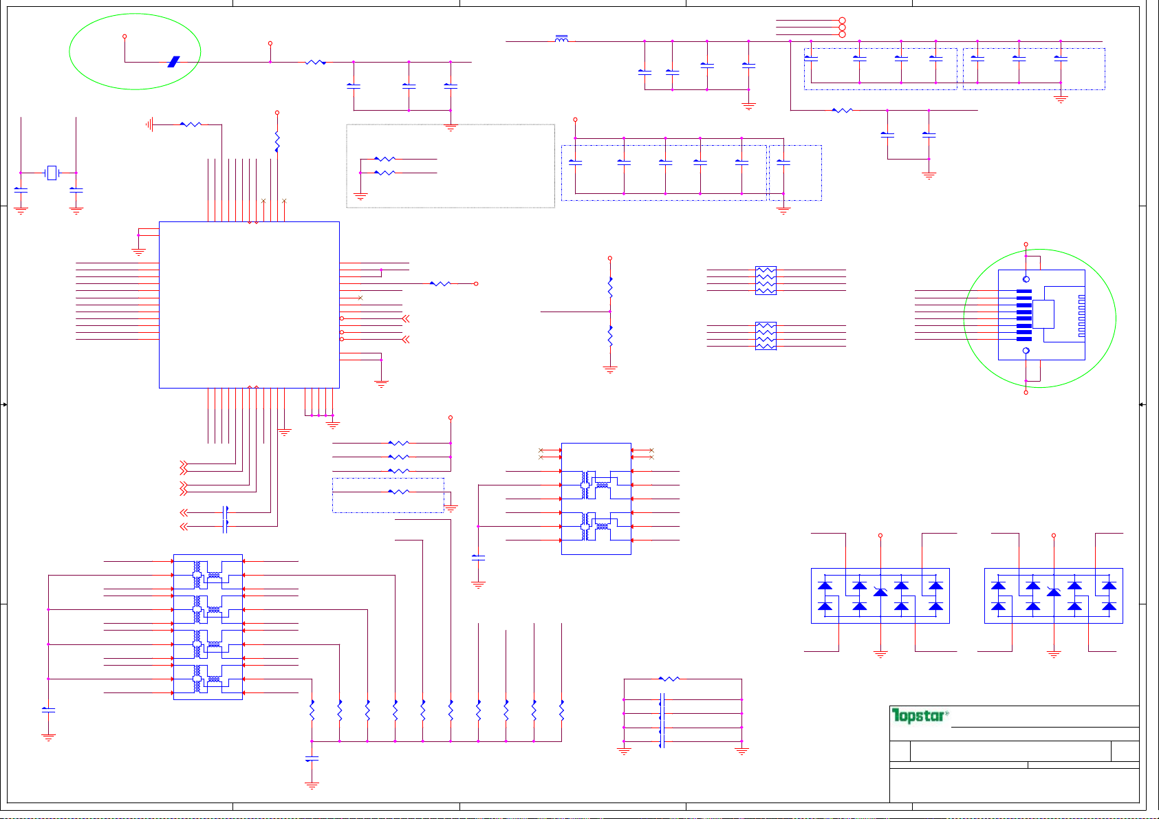
5
+V3.3LAN
650mA
1 2
FB31 300ohm@100MHz,2A
D D
XTAL1
1 2
C427
27pF/50V,NPO
C0402
C C
B B
A A
XTAL2
Y8 25MHz
XS2_3D3
C428
27pF/50V,NPO
C0402
C513
0.01uF/16V,X7R
C0402
RTL8111E
LAN_TX0+
LAN_TX0-LAN_TX0VDD10
LAN_TX1+
LAN_TX1VDD10
LAN_TX2+
LAN_TX2VDD10
LAN_TX3+
LAN_TX3Lan+V3.3AL
LAN_TX3-
LAN_TX3+
LAN_TX2-
LAN_TX2+
LAN_TX1-
LAN_TX1+
LAN_TX0-
LAN_TX0+
PCIE_TXP1_LAN16
PCIE_TXN1_LAN16
PCIE_GLAN_CLKP16
PCIE_GLAN_CLKN16
PCIE_RXP1_LAN16
PCIE_RXN1_LAN16
5
R633 2.49K,1%
U32
G1
G2
1
2
3
4
5
6
7
8
9
10
11
12
QFNS48_0D4_1G
R0402
G1
G2
MDIP 0
MDIN0
AVD D10_1
MDIP 1
MDIN1
AVD D10_2(NC )
MDIP 2(NC)
MDIN2(NC )
AVD D10_3(NC )
MDIP 3(NC)
MDIN3(NC )
AVD D33_4(NC )
350uH/0.5uH 1:1
1CT:1CT
2
TD1 +
1
TCT 1
3
TD1 -
1CT:1CT
5
TD2 +
4
TCT 2
6
TD2 -
1CT:1CT
8
TD3 +
7
TCT 3
9
TD3 -
1CT:1CT
11
TD4 +
10
TCT 4
12
TD4 -
FB0805
RSET
Lan+V3.3AL
Lan+V3.3AL
47
AVDD33_348AVDD33_2
DVDD10_1
SMBCLK(NC)14SMBDATA(NC)15CLKREQB
13
VDD10
SMBCLK_L
C438 0.1uF/10V,X7R
C439 0.1uF/10V,X7R
TRAN24_1_7D1
VDD10
XTAL2
46
45
RSET
AVDD10_5
16
SMBDATA_L
CLKREQ#
C0402
C0402
IOU1
MX1+
MCT1
MC1-
MX2+
MCT2
MX2-
MX3+
MCT3
MX3-
MX4+
MCT4
MX4-
RTL8111E
Lan+V3.3AL
Lan+V3.3AL
XTAL1
Lan+V3.3AL
Lan+V3.3AL
VDD10
43
42
41
40
39
LED0
CKXTAL244CKXTAL1
DVDD3_2
AVDD33_1
DVDD10_3(NC)
HSIP17HSIN18REFCLK_P19REFCLK_N20EVDD1021HSOP22HSON
EVDD10
23
TX3-
24
22
TX3+
20
TX2-
21
19
TX2+
17
TX1-
18
16
TX1+
14
TX0-
15
13
TX0+
The rise time must >1ms
R632 0
R634
1K
R0402
GPO
38
37
LED1/EESK
GPO/SMBALERT
VDD REG_2
VDD REG_1
ENSW REG
LED 3/EEDO
EEC S/SCL
DVD D10_2
LANW AKEB
DVD D33_1
ISO LATEB
GND
24
23
MCT3
MCT4
4
R0603
C413
C0805
4.7uf/10V
R636 10K R0402
R637 10K R0402
TU142 VerB: Removed LAN EEPROM 93C46/93C56 2011-12-20
1.05V noise must <150mV
36
REG OUT
EED I/SDA
PER STB
G3G3G4G4G5G5G6G6G7
MCT1
MCT2
R441
75
R0402
RTL8111E
C307
1000pF/2000V
C1206
CASE_GND
G9
G8
REGOUT
35
AVDD33_REG
34
33
ENSWREG
32
31
30
29
VDD10
28
27
Lan+V3.3AL
26
ISOLATEB
25
G9
G8
G7
SMBCLK_L
CLKREQ#
SMBDATA_L
SMBDATA_L
Strap for 93C46 ROM and efuse
R450
75
R0402
RTL8111E
RTL8111E
4
AVDD33_REG
C414
C0805
10uf/6.3V
ns
SCL
SDA
3.3V noise must <150mV
R638 0 R0402
SDA
SCL
PCIE_WAKE# 17,20,31
BUF_PLT_RST# 7,19,31,33
R641 1K R0402 ns
R642 10K R0402
R643 1K R0402 ns
R64410K R0402
MCT6
MCT5
R459
75
R0402
RTL8111E
R454
75
R0402
RTL8105E
R453
75
R0402
C415
C0402
0.1uF/10V,X7R
Lan+V3.3AL
R452
75
R0402
RTL8105E
Lan+V3.3AL
C306
0.01uF/16V,X7R
C0402
RTL8105E
RJ45_TX3-
R415
75
R0402
RTL8105E
REGOUT
LAN_TX1+
LAN_TX1-
LAN_TX0+
LAN_TX0-
RJ45_TX3+
R419
75
R0402
RTL8105E
RJ45_TX2-
L1
1
4.7uH/1.22A
LS2_3513
ISOLATEB
5
4
3
2
1
8
7
6
H16101ME
R424
75
R0402
RTL8105E
3
Lan+V3.3AL
C432
C0402
0.1uF/10V,X7R
IOU2
TRAN16_6D75
N4
N3
TD-
TDC
TD+
RD-
RDC
RD+
RTL8105E
ASSY
RJ45_TX2+
R426
75
R0402
RTL8105E
3
C419
C424
ns
ns
C0805
C0805
10uf/6.3V
10uf/6.3V
C433
C0402
0.1uF/10V,X7R
C434
C0402
0.1uF/10V,X7R
Close U33 Pin 27, 39, 42, 47, 48.
+V3.3S
R639
1K
R0402
R640
15K
R0402
13
N2
12
N1
14
TX1+
15
MCT5
16
TX1-
9
TX0+
10
MCT6
11
TX0-
R495 0 R0402
C105 330pF/50V,X7R C0402
C30 4.7uf/10V C0805
C104 330pF/50V,X7R C0402
C41 330pF/50V,X7R C0402
ns
1CT:1CT
1CT:1CT
TX-
CMT
TX+
RX-
RXC
RX+
2
C418
C0805
4.7uf/10V
C435
C0402
0.1uF/10V,X7R
C421
C0402
0.1uF/10V,X7R
C436
C0402
0.1uF/10V,X7R
0.1uF/10V,X7R
R635 0 R0402
C437
C0402
0.1uF/10V,X7R
RTL8111E
Close U33 Pin 12
RN2
1 2
TX0+ RJ45_TX0+
3 4
TX0-
5 6
TX1+
7 8
TX1-
RA0603_8
RN1
1 2
TX2+
3 4
TX2-
5 6
TX3+
7 8
TX3- RJ45_TX3-
RTL8111E
RA0603_8
CASE_GND
RJ45_TX0-
RJ45_TX1+
RJ45_TX1-
0
RJ45_TX2+
RJ45_TX2RJ45_TX3+
0
LD1
AOZ8902CIL
SOT23_6
RTL8111E
LAN_TX2- LAN_TX2+
2
+V3.3S 7,14,15,16,17,18,19,20,21,22,24,25,29,30,31,32,33,35,40,41,42,43,44,45,47
+V3.3AL 7,15,16,17,19,20,22,24,28,31,33,40,43,45
+V3.3LAN 31
1uf/10V
C0402
C429
C420
C0402
0.1uF/10V,X7R
0.1uF/10V,X7R
C425
C0402
0.1uF/10V,X7R
EVDD10
C430
C0402
RJ45_TX0+
RJ45_TX0RJ45_TX1+
RJ45_TX2+
RJ45_TX2RJ45_TX1RJ45_TX3+
RJ45_TX3-
C422
C0402
0.1uF/10V,X7R
RTL8111E
Close U33 Pin 6, 9,41
CASE_GND
RJ45
1
TX0+
2
TX0-
3
TX1+
4
TX2+
5
TX2-
6
TX1-
7
TX3+
8
TX3-
CASE_GND
C416
C0402
C417
C0402
0.1uF/10V,X7R
Close U33 Pin 3, 13, 29, 45.
0607:Change RJ45 CONN follow TU151.-Zhouzm
Lan+V3.3AL Lan+V3.3AL
4
5
3
2
LAN_TX3+
6
1
Page Name
Page Name
Page Name
Size
Size
Size
Project Name Rev
Project Name Rev
Project Name Rev
A3
A3
A3
Date: Sheet of
Date: Sheet of
Date: Sheet of
PROPERTY NOTE: this document contains information confidential and property to
PROPERTY NOTE: this document contains information confidential and property to
PROPERTY NOTE: this document contains information confidential and property to
TOPSTAR and shall not be reproduced or transferred to other documents or disclosed
TOPSTAR and shall not be reproduced or transferred to other documents or disclosed
TOPSTAR and shall not be reproduced or transferred to other documents or disclosed
to others or used for any purpose other than that for which it was obtained without
to others or used for any purpose other than that for which it was obtained without
to others or used for any purpose other than that for which it was obtained without
the expressed written consent of TOPSTAR
the expressed written consent of TOPSTAR
the expressed written consent of TOPSTAR
LAN_TX1-
LD2
AOZ8902CIL
SOT23_6
3
LAN_TX0- LAN_TX0+
TOPSTAR TECHNOLOGY
TOPSTAR TECHNOLOGY
TOPSTAR TECHNOLOGY
Robin
Robin
Robin
LAN(RTL8105E/8111E)
LAN(RTL8105E/8111E)
LAN(RTL8105E/8111E)
TU142 PVT
TU142 PVT
TU142 PVT
1
C426
C0402
0.1uF/10V,X7R
RTL8111E
910
1112
4
1
0.1uF/10V,X7R
RJ1
TX0+
TX0TX1+
TX2+
TX2TX1TX3+
TX3-
RJ45_SE_A
RJ45
5
2
34 51Wednesday, January 09, 2013
34 51Wednesday, January 09, 2013
34 51Wednesday, January 09, 2013
VDD10
C423
C0402
RTL8111E
ASSY
LAN_TX1+LAN_TX3-
6
1
C
C
C
Page 35
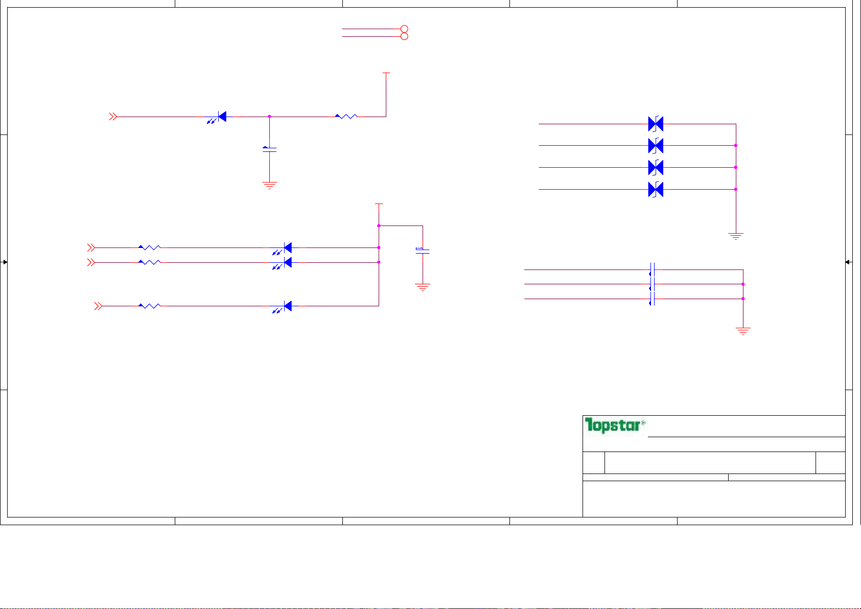
5
4
3
+V3.3S 7,14,15,16,17,18,19,20,21,22,24,25,29,30,31,32,33,34,40,41,42,43,44,45,47
+V3.3SB 7,15,17,20,22,28,31,33,37,38,39,45
2
1
D D
LED
+V3.3S
White color
WLA N1 LTW -C193SN5
WIRELESS_LED #31
C C
CHG_LED#33
BTL_LED#33
POW ERLED #33
B B
680R 345
R0402
680R 344
R0402
680R 346
R0402
CHAR GE_LED
BAT_STATE_LED
PWR_LED
12
LED2_0603
C278
1000pF/50V,X7R
C0402
WLA N+
CHAR GE1
LTST-C193KFKT-5A/2.0V/Amber
LED2_0603
BTL_LED LTW -C193SN5
POW ER1 LTW-C 193SN5
AMB
12
12
LED2_0603
White
12
LED2_0603
White color
680R 343
R0402
+V3.3SB
C279
0.1UF/10V,X7R
C0402
WIRELESS_LED #
CHAR GE_LED
BAT_STATE_LED
PWR_LED
BAT_STATE_LED
CHAR GE_LED
PWR_LED
1 2
ESD1 EGA10603V05A 1-B
1 2
ESD4 EGA10603V05A 1-B
1 2
ESD2 EGA1-0603-V05
1 2
ESD3 EGA1-0603-V05
C280 1000pF/50V,X7R C0402
C281 1000pF/50V,X7R C0402
C282 1000pF/50V,X7R C0402
ESDPAD _R0402ns
ESDPAD _R0402ns
ESDPAD _R0402ns
ESDPAD _R0402ns
TOPSTAR TECHN OLOGY
TOPSTAR TECHN OLOGY
TOPSTAR TECHN OLOGY
Robin
Robin
Page Name
Page Name
Page Name
A A
5
4
3
Size
Size
Size
Project N ame Rev
Project N ame Rev
Project N ame Rev
Custom
Custom
Custom
Date: Sheet of
Date: Sheet of
Date: Sheet of
PROPERTY NOTE: this d ocument contains i nformati on confid ential and prop erty to
PROPERTY NOTE: this d ocument contains i nformati on confid ential and prop erty to
PROPERTY NOTE: this d ocument contains i nformati on confid ential and prop erty to
TOPSTAR and shall not b e reproduced or transferred to other d ocuments or disclosed
TOPSTAR and shall not b e reproduced or transferred to other d ocuments or disclosed
TOPSTAR and shall not b e reproduced or transferred to other d ocuments or disclosed
to others or used for any purp ose other than that for which it was obtained without
to others or used for any purp ose other than that for which it was obtained without
to others or used for any purp ose other than that for which it was obtained without
the express ed wr itten consent of TOPST AR
the express ed wr itten consent of TOPST AR
the express ed wr itten consent of TOPST AR
2
Robin
LED
LED
LED
TU142 PV T
TU142 PV T
TU142 PV T
C
C
C
35 51Wed nesday, January 09, 2013
35 51Wed nesday, January 09, 2013
35 51Wed nesday, January 09, 2013
1
Page 36

5
USB 3.0 Connector
USB3_+V5AL1
12
D18
D D
USB4
1
VBUS
2
D-
3
D+
4
Shield4
Shield3
Shield2
Shield1
GND_DRAIN
GND
SSRX-
SSRX+
SSTX-
SSTX+
5
6
7
8
9
13
12
11
10
C C
USB3.0
USB3D0_1
ASSY
ESDPAD_R0402
EGA1-0603-V05
-DATA0
+DATA0
A_URXN_C0
A_URXP_C0
A_UTXN_C0
A_UTXP_C0
C443
ns
CHK8
90Ω/100MHz 0.5A
L4_0805_SHORT
ns
USB Interface power supply changed due to change of OC.
TU142 VerC.
4
C182
C0402
ns
C0402
330PF/50V,X7R
0.01uF/16V,X7R
R781 0 R0402
R780 0 R0402
R789 0 R0402 USB Debug
R790 0 R0402 USB Debug
43
C510 0.1UF/10V,X7R
12
Co-Lay3A
12
1
CAP6D3X7A
+
C377
220uF/6.3V
ASSY
CHK7
43
90Ω/100MHz 0.5A
12
L4_0805_SHORT
ns
C0402
USB3.0
USB3.0
C0402
C511 0.1UF/10V,X7R
S2 1.6AFUSE1812
1 2
1 2
S1
300KR576
R0402
USB_PN0 19
USB_PP0 19
USB_PN9 19
USB_PP9 19
USB2.0
FUSE1812
2.6A
USB3.0
R579
560K
R0402
1000pF/50V,X7R
USB3_RX1_N 19
USB3_RX1_P 19
USB3_TX1_N 19
USB3_TX1_P 19
+V5AL
C380
C0402
ns
3
USB_OC#0 19
A_URXN_C0
A_URXP_C0
A_UTXN_C0
A_UTXP_C0
-DATA0
+DATA0
D25
EGA1-0603-V05
ESDPAD_R0402
12
12
U36
1
D1+
2
D1-
3
GND1
4
D2+
D2-5NC1
TPD4EUSB30DQAR
SON10_0D5_1
USB3.0
NC4
NC3
GND2
NC2
2
D24
EGA1-0603-V05
ESDPAD_R0402
10
9
8
7
6
+V5AL 24,33,39,41,43,45,46,47
A_URXN_C0
A_URXP_C0
A_UTXN_C0
A_UTXP_C0
1
A_URXN_C1
A_URXP_C1
A_UTXN_C1
A_UTXP_C1
-DATA2
+DATA2
D40
EGA1-0603-V05
ESDPAD_R0402
12
12
U38
1
D1+
2
D1-
3
GND1
4
D2+
D2-5NC1
TPD4EUSB30DQAR
SON10_0D5_1
USB3.0
D39
EGA1-0603-V05
ESDPAD_R0402
NC4
NC3
GND2
NC2
10
A_URXN_C1
9
A_URXP_C1
8
7
A_UTXN_C1
6
A_UTXP_C1
TOPSTAR TECHNOLOGY
TOPSTAR TECHNOLOGY
TOPSTAR TECHNOLOGY
Robin
Robin
Page Name
Page Name
Page Name
Size
Size
Size
Project Name Rev
Project Name Rev
Project Name Rev
B
B
B
Date: Sheet of
Wednesday, January 09, 2013
Date: Sheet of
Wednesday, January 09, 2013
Date: Sheet of
Wednesday, January 09, 2013
PROPERTY NOTE: this document contains information confidential and property to
PROPERTY NOTE: this document contains information confidential and property to
PROPERTY NOTE: this document contains information confidential and property to
TOPSTAR and shall not be reproduced or transferred to other documents or disclosed
TOPSTAR and shall not be reproduced or transferred to other documents or disclosed
TOPSTAR and shall not be reproduced or transferred to other documents or disclosed
to others or used for any purpose other than that for which it was obtained without
to others or used for any purpose other than that for which it was obtained without
to others or used for any purpose other than that for which it was obtained without
the expressed written consent of TOPSTAR
the expressed written consent of TOPSTAR
the expressed written consent of TOPSTAR
2
Robin
USB CONN
USB CONN
USB CONN
TU142 PVT
TU142 PVT
TU142 PVT
C
C
C
5237
5237
5237
1
USB3_+V5AL1
12
D38
ns
C444
C0402
0.01uF/16V,X7R
43
12
CHK9
90Ω/100MHz 0.5A
L4_0805_SHORT
ns
4
CHK11
90Ω/100MHz 0.5A
43
12
L4_0805_SHORT
ns
CHK10
C535 0.1UF/10V,X7R
C0402
C534 0.1UF/10V,X7R
C0402
90Ω/100MHz 0.5A
L4_0805_SHORT
43
12
ns
USB3.0
USB3.0
USB_PN1 19
USB_PP1 19
USB3_RX2_N 19
USB3_RX2_P 19
USB3_TX2_N 19
USB3_TX2_P 19
3
ESDPAD_R0402
EGA1-0603-V05
B B
USB5
1
VBUS
2
D-
3
D+
4
Shield4
Shield3
Shield2
Shield1
GND_DRAIN
GND
SSRX-
SSRX+
SSTX-
SSTX+
5
6
7
8
9
13
12
11
10
USB3.0
USB3D0_1
ASSY
A A
5
-DATA2
+DATA2
A_URXN_C1
A_URXP_C1
A_UTXN_C1
A_UTXP_C1
Page 37
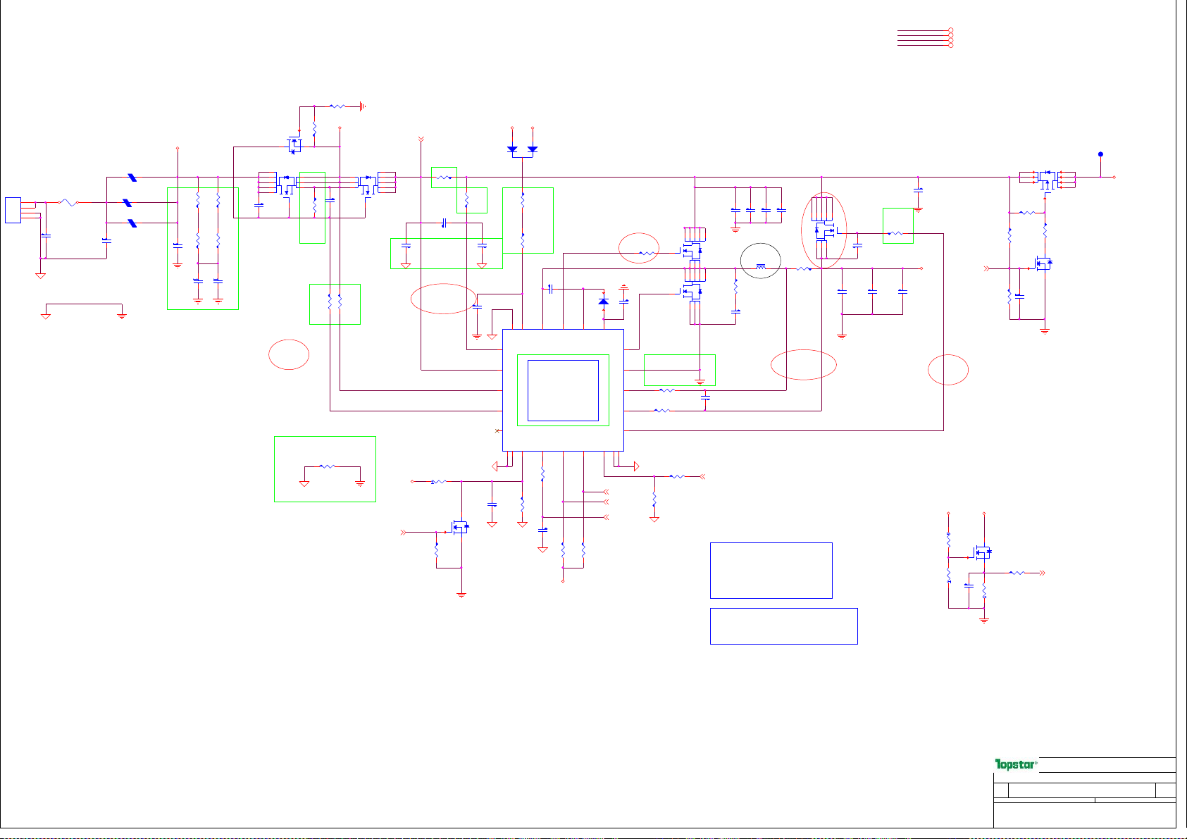
18.5-19V/4A
AD_IN
1
1
2
2
3
3
4
4
Wafer
CND4_2D5_R
ASSY
GND_JACK
GND_JACK
1 2
FUSE1206
PC4
0.1uF/25V,X7R
C0603
GND_JACK
PF1
7A 32V
100ohm@100MHz,3A
HV_ACIN
4A
1 2
PC355
C0805
1uf/25V
通过开桥与大地连接
PFB4
1 2
PFB5
100ohm@100MHz,3A
PFB6
1 2
100ohm@100MHz,3A
FB0805
FB0805
FB0805
1uf/25V
PC354
C0805
+VDC 24,39,40,41,44,47
AD+ 39
BATT+ 38
+V3.3SB 7,15,17,20,22,28,31,33,35,38,39,45
PR376
300K
R0402
PQ74
LBSS138LT1G
sot23
AD+
PR380
PR379
2.2
2.2
R0805
R0805
ns
PR2
PR5
2.2
2.2
R0805
R0805
ns
PC120
PC104
C0805
C0805
1uf/25V
1uf/25V
312
PQ2
AON7410
9
SO8_26_130
8
7
6
5
D
G
4
PC316
2200pF/25V,X7R
C0402
靠近对应
MOS
管摆放。走线为高压线
19-25V
,拉开与其它线
15mil
LAYOUT NOTE:
靠近
AD++
PR377
1M
R0402
AON7410
PC317
C0603
0.1uF/25V,X7R
HV_CMSRC1
HV_ACDRV1
PR387
4.02K,1%
R0402
SO8_26_130
1
2
3
S
G
4
1
2
3
S
PR478
510K
R0402
add PR478
PR386
4.02K,1%
R0402
以上距离
要避免在 大电流路 径单点 接连
PC332
单点接地
PR409
0
R0402
CHG_GND
HV_Isense_SYSP28
PQ6
4A
9
8
7
6
5
D
PC326
0.1uF/25V,X7R
C0603
CHG_GND CHG_GND
差分等长走线,
从取样电阻焊盘处引线。
避开干扰区域走线。
HV_CMSRC
HV_ACDRV
AD+
AC_OFF33
PR402
510K
PR381
20mohm,1%
R1206
PC324
0.1uF/25V,X7R
C0603
R0402
PQ79
L2N7002LT1G
SOT23
1
PR398
100K
R0402
3
2
PR382
0
R0402
HV_ACN
1uf/25V
C0805
CHG_GND
CHG_GND
PC335
0.01uF/16V,X7R
C0402
PC327
0.1uF/25V,X7R
C0603
1
ACN
2
ACP
3
CMSRC
4
ACDRV
5
ACOK
PR400
80.6K,1%
R0402
CHG_GNDCHG_GND
AD+ BATT+
HV_Isense_SYSN
PR475
10
R0805
PR476
10
R0805
20
G5
VCC
GND5
GND1G1GND2
6
G2
PC334
100pF/50V,NPO
C0402
CHG_GND
132
PD23
LBAT54CLT1G
sot23
19
QFNS20_0D5_1G
PC325
0.1uF/25V,X7R
C0603
PHASE
PU4
BQ24735
IOUT7ACDET
PR410
100
R0402
+V3.3SB
HV_HG_Charger
PD25
1N5819W DIODESEMI
SOD123
17
18
BTST
HIDRV
SDA8SCL9ILIM
PR405
PR404
10K
R0402
R0402
所有驱动线电阻
靠近对应
MOS
1
16
REGN
LODRV
GND
SRP
SRN
BATDRV
10
SM_CHG_SCL2 33
SM_CHG_SDA2 33
SYS_I_Sense 33
10K
Layout
管摆放。
HV_LL_Charger
1uf/10V
15
14
13
12
11
GND3G3GND4
G4
PR391
R0402
时
0
PC329
C0402
LG_Charg er
CHG_GND
CHG_GND
4
4
PQ9
AON7410
SO8_26_130
R815
R816
10
R0402
4.7
R0402
PR406
510K
R0402
PR401
75K
R0402
D
G
D
G
4A
PC319
1000pF/50V,X7R
C0402
56789
PQ3
AON7410
SO8_26_130
S
123
56789
S
123
PC333
0.1UF/10V,X7R
C0402
CHG_ON 33
SYS_ I_S ens e
0.2V
0.6V
ACDE T>2 .4V ,AD+ >=1 7.5 V
ILIM=0.42V,
PC192
4.7uF/25V SAMSUNG
PC320
PC8
4.7uF/25V SAMSUNG
C0805
PL12
1
4.7uH/5.5A
PR395
LS2_6530
2.2
R0805
PC330
1000pF/50V,X7R
C0402
C0805
ns
0.1uF/25V,X7R
C0603
SYS_ CUR REN T
3.33A0.66V
硬件电路设定最大充电电流
PR393
10mohm,1%
R1206
1A
3A
4A0.8V
6A
30mohm @4.5V
需打孔到内层多层铺铜加强散热。
56789
PQ76
D
AON7410
SO8_26_130
4
G
S
123
PC322
C0402
0.01uF/25V,X7R
PC345
4.7uF/25V SAMSUNG
C0805PC332
PC346
4.7uF/25V SAMSUNG
C0805
差分等长走线,
从取样电阻焊盘处引线。
避开干扰区域走线。
HV_BATDRV
2.1A
6A
PR388
4.02K,1%
R0402
12.6V
2A
Max
PC328
0.1uF/25V,X7R
C0603
PC315
0.1UF/25V,X7R
C0603
BATT+
PR413
510K
R0402
PC342
1000pF/50V,X7R
C0402
HV_SHDN#43
走线为高压线
拉开与其它线
PR412
510K
R0402
1
VDC1
TestP
ns
TPC60
8
7
6
5
+VDC
9V-1 9V/ 6A
PR389
51K
R0402
PR383
510K
R0402
1
PQ82
AP4407
SO8_50_150
1
2
3
S
D
G
4
PR390
100K
R0402
3
PQ78
L2N7002LT1G
SOT23
2
PR397
200K
PC331
R0402
1000pF/50V,X7R
C0402
18V
,
10mil
以上距离
+V3.3SBAD+
3
PQ81
L2N7002LT1G
SOT23
2
PR415
47K
R0402
PR414
1K
R0402
AC_IN 33
TOPSTAR TECHNOLOGY
TOPSTAR TECHNOLOGY
TOPSTAR TECHNOLOGY
Page Name
Page Name
Page Name
Size
Size
Size
Project Name Rev
Project Name Rev
Project Name Rev
A2
A2
A2
Date: Sheet of
Date: Sheet of
Date: Sheet of
PROPERTY NOTE: this document contains information confidential and property to
PROPERTY NOTE: this document contains information confidential and property to
PROPERTY NOTE: this document contains information confidential and property to
TOPSTAR and shall not be reproduced or transferred to other documents or disclosed
TOPSTAR and shall not be reproduced or transferred to other documents or disclosed
TOPSTAR and shall not be reproduced or transferred to other documents or disclosed
to others or used for any purpose other than that for which it was obtained without
to others or used for any purpose other than that for which it was obtained without
to others or used for any purpose other than that for which it was obtained without
the expressed written consent of TOPSTAR
the expressed written consent of TOPSTAR
the expressed written consent of TOPSTAR
Power path/Charger
Power path/Charger
Power path/Charger
CL42 EVT
CL42 EVT
CL42 EVT
37 51Wednesday, January 09, 2013
37 51Wednesday, January 09, 2013
37 51Wednesday, January 09, 2013
A
A
A
Page 38

BATT+
PFB2
100ohm@10 0MHz,3A
1 2
FB0805
PFB3 100ohm@100 MHz,3A
1 2
FB0805
SM_BAT_SDA233
SM_BAT_SCL233
240mils.
PFB1
1 2
100ohm@10 0MHz,3A
FB0805
PC15
5.6pF/50V,NPO
C0402
6A 8A
PC117
1000pF/50V,X7R
C0402
内层桥接走线,宽度保证有
PC14
0.1uF/25V,X7R
C0603
1 2
12A 24V 6mΩ FUSE120 6
100PR13
R0402
100
PR3 R0402
PC3
5.6pF/50V,NPO
C0402
FP1
SM_BAT_SDA
SM_BAT_SCL
+V3.3SB
PR161
300K
R0402
GND_BAT
BATT+ 37
+V3.3SB 7 ,15,17,20,22,28,3 1,33,35,37,39,45
CL341 VerC: Add PC10/PC14, EMI Request 2012/12/25
PC10
0.1uF/25V,X7R
C0603
BATCON1
Wafer
CNS9_R
9
BAT+
8
BAT+
7
BAT+
6
BAT_D
5
BAT_C
4
BAT_IN
3
GND
2
GND
1
GND
6A
0.1uF/10V,X7R
GND11GND
10
0.1uF/10V,X7R
PC16
C0402
PC9
C0402
+V3.3SB
+V3.3SB
LBAT54SLT1G
sot23
2
1
PZD2
LBAT54SLT1G
sot23
2
1
PZD1
3
SM_BAT_SDA
3
SM_BAT_SCL
GND_BAT
R0402
1KPR163
BATT_IN# 33
TOPSTAR TECHNOLOGY
TOPSTAR TECHNOLOGY
TOPSTAR TECHNOLOGY
Robin
Robin
Page Name
Page Name
Page Name
Size
Size
Size
Project Name Rev
Project Name Rev
Project Name Rev
Custom
Custom
Custom
Date: Sheet of
Date: Sheet of
Date: Sheet of
PROPERTY NOTE: this document contains information confidential an d proper ty to
PROPERTY NOTE: this document contains information confidential an d proper ty to
PROPERTY NOTE: this document contains information confidential an d proper ty to
TOPSTAR and shall not be repr oduced or tra nsferred to other documents or disclosed
TOPSTAR and shall not be repr oduced or tra nsferred to other documents or disclosed
TOPSTAR and shall not be repr oduced or tra nsferred to other documents or disclosed
to others or used for any pu rpose other than that for which it was obtained without
to others or used for any pu rpose other than that for which it was obtained without
to others or used for any pu rpose other than that for which it was obtained without
the expressed written consent of TOPSTAR
the expressed written consent of TOPSTAR
the expressed written consent of TOPSTAR
Robin
BATTERY IN
BATTERY IN
BATTERY IN
TU142 PVT
TU142 PVT
TU142 PVT
38 51Wednesday, January 09, 20 13
38 51Wednesday, January 09, 20 13
38 51Wednesday, January 09, 20 13
C
C
C
Page 39
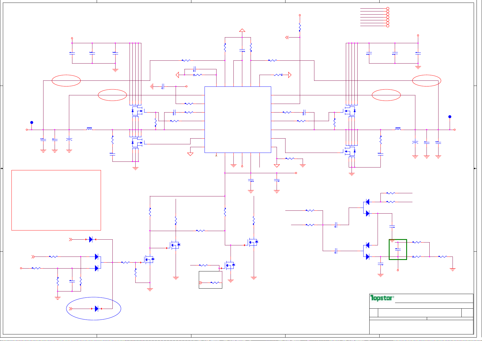
5
+VDC
D D
PC193
4.7uF/25V SAMSUNG
C0805
2A 2A
PC5
0.1uF/25V,X7R
C0603
PC6
1000pF/50V,X7R
C0402
电压反馈线,避开干扰区走线。
放电路径,从电容处单独走线。
V3R3SB1
TestP
ns
TPC60
C C
+V3.3SB
PC22
4.7uf/10V
C0805
ns
CAP6D3X7A
PC128
220uF/6.3V
PC21
1000pF/50V,X7R
C0402
PL1
3.3uH/4.8A
LS2_8836
HV_LL_3.3V
12
1
+
1
SO8_26_130
PR10
2.2
R0805
ns
PC2
1000pF/50V,X7R
C0402
ns
PQ11
AON7410
Buck/Boost电路基本Layout要求
1.输入电容两极要分别靠近上管D极,下管S极摆放。
2.MOS管尽量靠近IC芯片,驱动线不要过长。
3.芯片的Thermal
GND用至少5个过孔连到信号地,用来散热
4.信号地和电源地在输出电容的负极连到一起
5、下管驱动线要避开phase区,并避免和
B B
上管驱动线、驱动返回线平行
6、续流二极管尽量以下管摆放在一起
7、以HV开头的net,要保证和其它线间距10mil以上。
8、上管驱动线电阻靠近上管放置。
PWR_SW_VCC228
PR96
10
R0402
PR174
200K
R0402
PR173
51K
R0402
ALWAYS_ON33,45,46
AD+
A A
PM_SLP_S4#33,45
ALW_ON
PC122
0.22uF/16V,X7R
C0603
1
PD15
LRC LMDL914T1G 100V 200mA
SOD323
2
1
PR20
200K
R0402
1
LRC LMDL914T1G 100V 200mA
3
PD14
LBAT54CLT1G
sot23
PD17
SOD323
ns
PR22
1K
R0402
PR18
510K
R0402
F42 VerB: Add PM_SLP_S4# to control +V3.3SB enable for deep S3 20110824
5
4
PR158
7.68K,1%
R0402
PR160
5.11K,1%
R0402
GND_TPS51125
PC1
123
123
56789
S
56789
S
1
PR17
D
10K
R0402
4
G
D
4
G
PQ12
AON7410
SO8_26_130
3
10uf/6.3V
C0805
PC109
0.1uF/25V,X7R
C0603
PR12
47K
R0402
1
PQ7
L2N7002LT1G
SOT23
PR15
R0402
0
LG_3.3V
ENTRIP2
3
2
EC_RTC
PR154
100 R0402
PR156
2.2
R0402
HV_HG_3.3V
HV_LL_3.3V
GND_TPS51125
PR4
1K
R0402
PQ4
L2N7002LT1G
SOT23
2
PM_SLP_SUS#17,33,45
F42 Verc: Add PM_SLP_Sus# to control +V5AL enable for DS3
Swain 111206
4
2V 2V
PC110
0.1uF/10V,X7R
C0402
ENTRIP2
200KPR155 R0402
6
7
VO2
ENTRIP2
8
VRE G3
9
VBS T2
10
DRV H2
11
LL2
12
DRV L2
G2
GND2
EN0
13
PR100
0
R0402
ns
PR23
0
R0402 noDS3
ALW_ON
PR28
1K
R0402
DS3
1
3
GND_TPS51125
PC114
0.22uF/16V,X7R
C0603
4
5
VFB2
TONSEL
PU3
TPS51125
QFNS24_0D5_1G
SKIPSEL14GND15VIN16VREG5
+VDC
PR101
47K
R0402
3
PQ25
L2N7002LT1G
SOT23
2
3
PR162
10K,1%
R0402
VREF
2
3
VFB1
VREF
17
VREG5
PC113
4.7uf/10V
C0805
ENTRIP1
3
1
2
ALW_PWROK33
PR164
15K,1%
R0402
ENTRIP1
1
VO1
ENTRIP1
PGO OD
VBS T1
DRV H1
LL1
DRV L1
GND1
VCLK
18
VCLK
GND_TPS51125
PR168
1K
R0402
PQ8
L2N7002LT1G
SOT23
PR167
200K
R0402
24
23
22
21
20
19
G1
PR170
2.2
R0402
HV_HG_5V
PR6 0
R0402
PC116
10uf/6.3V
C0805
LG_5V
+V3.3SB
GND_TPS51125
PR14
0 R0402
HV_LL_5V
LG_5V
+VREG5
VCLK
PR165
47K
R0402
PC119
0.1uF/25V,X7R
C0603
PR374
R0402 8205M
0
PR284
R0402
0
TPS51125
2
PQ10
AON7410
SO8_26_130
4
PR16
10K
R0402
PQ14
AON7410
SO8_26_130
4
PC130
0.1uF/25V,X7R
C0603
6V_LED_Panel(min)
PC123
0.1uF/25V,X7R
C0603
6V_LED_Panel(min)
2
56789
D
G
S
56789
D
G
S
HV_12V_D
HV_12V_R1
1
+V3.3SB 7,15,17,20,22,28,31,33,35,37,38,45
+VDC 24,37,40,41,44,47
AD+ 37
+V5AL 24,33,36,41,43,45,46,47
EC_RTC 15,27,45
+VREG5 40
PC20
1000pF/50V,X7R
C0402
+12V 24,27,45,46
PC19
0.1uF/25V,X7R
C0603
+VDC
PC347
4.7uF/25V SAMSUNG
C0805
电压反馈线,避开干扰区走线。
放电路径,从电容处单独走线。
PL3
123
123
sot23
LBAT54SLT1G
1
PD18
3
2
6V_LED_Panel(min)
sot23
LBAT54SLT1G
1
PD19
3
2
6V_LED_Panel(min)
6V_LED_Panel(min)
Page Name
Page Name
Page Name
Size
Size
Size
A3
A3
A3
Date: Sheet of
Date: Sheet of
Date: Sheet of
PROPERTY NOTE: this document contains information confidential and property to
PROPERTY NOTE: this document contains information confidential and property to
PROPERTY NOTE: this document contains information confidential and property to
TOPSTAR and shall not be reproduced or transferred to other documents or disclosed
TOPSTAR and shall not be reproduced or transferred to other documents or disclosed
TOPSTAR and shall not be reproduced or transferred to other documents or disclosed
to others or used for any purpose other than that for which it was obtained without
to others or used for any purpose other than that for which it was obtained without
to others or used for any purpose other than that for which it was obtained without
the expressed written consent of TOPSTAR
the expressed written consent of TOPSTAR
the expressed written consent of TOPSTAR
5.2uH/5.5A
LS2_1051
1
PR169
2.2
CAP6D3X7A
R0805
PC144
ns
220uF/6.3V
PC118
1000pF/50V,X7R
C0402
ns
PR304
R0402 ns
VREG5
0
PR267
R0402
+V3.3SB
0
6V_LED_Panel(min)
HV_12V_R
PC129
0.1uF/25V,X7R
C0603
VCLK
C5
C0402
100pF/50V,NPO
ns
PC147
1uf/25V
C0805
+12V
Project Name Rev
Project Name Rev
Project Name Rev
PC148
4.7uf/10V
C0805
ns
12
1
+
PR375
R0402
0
8205M
R813
R0402
200K
8205M
TOPSTAR TECHNOLOGY
TOPSTAR TECHNOLOGY
TOPSTAR TECHNOLOGY
+V3.3AL/+V5AL
+V3.3AL/+V5AL
+V3.3AL/+V5AL
CL42 EVT
CL42 EVT
CL42 EVT
1
PC150
1000pF/50V,X7R
C0402
R814
47K
R0402
8205M
39 51Wednesday, January 09, 2013
39 51Wednesday, January 09, 2013
39 51Wednesday, January 09, 2013
V5AL1
TestP
ns
TPC60
+V5AL
5A5A
A
A
A
Page 40
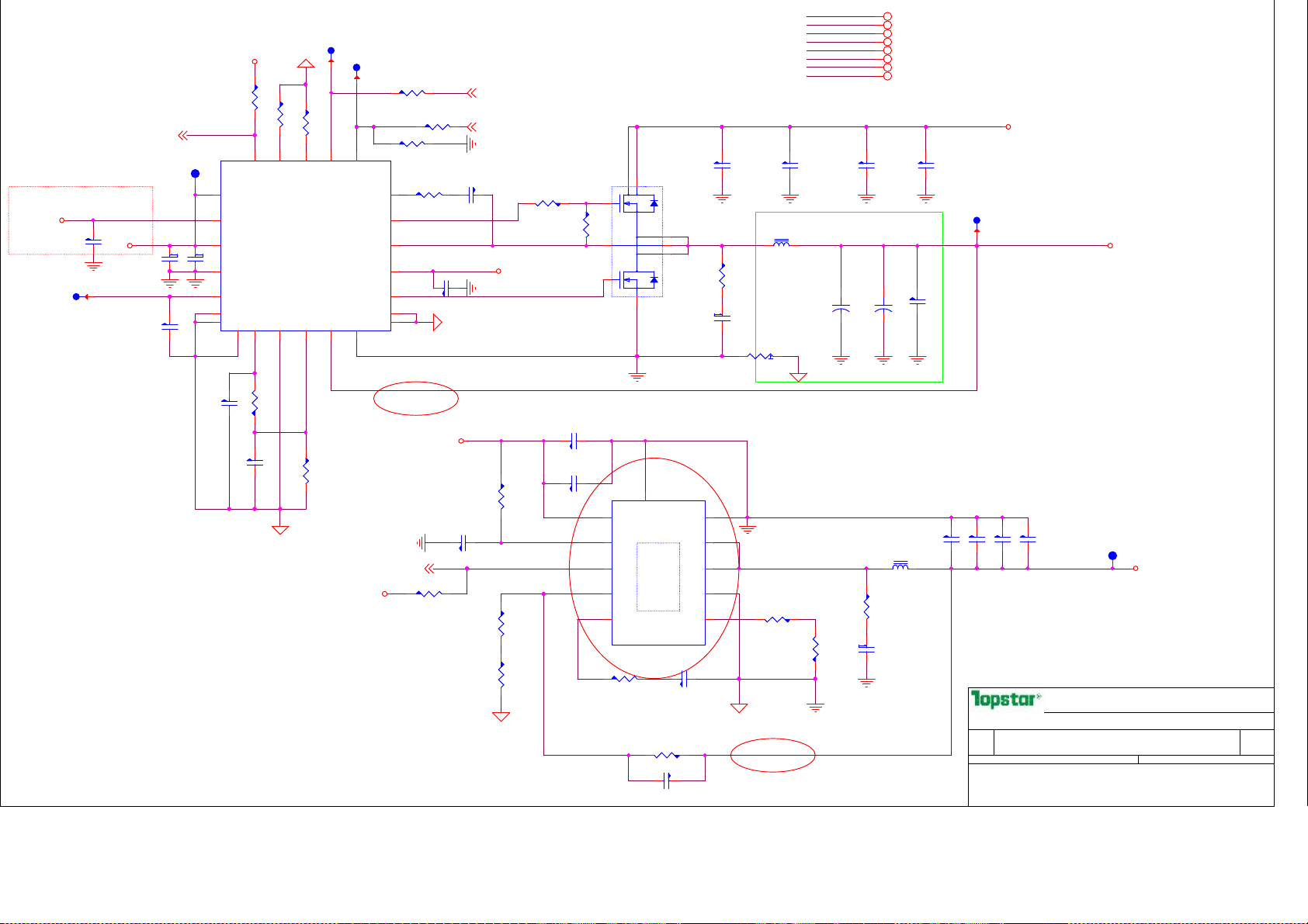
Pin2,Pin3走线1A
LDO
线路供电输入输出脚。
+V1.5
PC69
C0805
4.7uf/10V
VTTREF1
,注意走线宽度要求
+V0.75S
1A
10uf/6.3V
C0805
ns
0.22uF/16V,X7R
1A
PC94
ns
PC111
C0603
V0_75S1
TestP
TPC60
ns
PC93
10uf/6.3V
C0805
PR121
47K
R0402
1
VTTSNS
2
VLDOIN
3
VTT
4
VTTGND
5
VTTREF
G1
G1
G2
G2
PC115
0.1uF/10V,X7R
C0402
PC112
0.01uF/16V,X7R
C0402
+V3.3AL
GND_VDDQ
PR123
68K
R0402
19
20
G3
18
MODE
PGOOD
PU7
TPS51216
qfns20_0d4_1g
VREF6GND7REFIN8VDDQSNS9PGND
G3
PR157
1.02K,1%
R0402
GND_VDDQ
V0_75S_ON
ns
PR124
100K
R0402
TRIP
PR153
5.11K,1%
R0402
17
V1_5_ON
ns
S516S3
VBST
DRVH
DRVL
10
+V3.3S
Rmode=68K.设定f=300KHz,
PR126
2K
R0402
PR477
100K
R0402
15
14
13
SW
12
V5IN
11
G5
G5
G4
G4
V1.8S_PWG43
以及放电模式为
V0_75S_ON 33
PR125
2K
PR138
0
R0603
R0402
PC106
4.7uf/10V
C0805
HV_HG_VDDQ
PC105
0.1uF/25V,X7R
C0603
GND_VDDQ
V1_5_ON 33DDR_PWG43
HV_LL_VDDQ
+VREG5
电压反馈线,避开干扰区走线。
+V5S
2A
PR251
1
R0603
GND_8015B
0.1uF/10V,X7R
PR252
10K
R0402
PC185
C0402
LG_VDDQ
PR254
20K
R0402
PR255
220K
R0402
non-tracking mode.
PR278
0
R0603
CSD87352 2N 30V
SON8_1D27_1D6G
PC177
10uf/6.3V
C0805
PC181
10uf/6.3V
C0805
0.8V
3
PR277
10K
R0402
4
5
6
7
8
9
10
2
1
D1
G1
S1
D2
G2
S2
9
11
PVDD
VDD
PGOOD
FB
COMP
1M-1.2MHz
PR248
22k
R0402
PQ87
8
7
6
PU9
RT8015B
QFN10_0D5_0D8G
G1
PGND
LX2
LX1
GND
SHDN/RT
PC182
1000pF/50V,X7R
C0402
PR253
300K
R0402
PC186
22pF/50V,NPO
C0402
+V0.75S 14,45
+VREG5 39
+V3.3AL 7,15,16,17,19,20,22,24,28,31,33,43,45
+VDC 24,37,39,41,44,47
+V1.5 7,14,45
+V5S 15,16,22,24,25,27,28,29,30,42,44,45,47
+V1.8S 10,20,21,45
+V3.3S 7,14,15,16,17,18,19,20,21,22,24,25,29,30,31,32,33,34,35,41,42,43,44,45,47
12
1
+
PC96
560uF/2.5V/7mohm
CAP6D3X7A
PC204
4.7uF/25V SAMSUNG
C0805
16A
12
1
PC198
0.1uF/10V,X7R
+
C0402
PC102
0.1uF/25V,X7R
C0603
PL11
1
1.0uH/11A
LS2_6530
PR137
2.2
R0805
PC103
1000pF/50V,X7R
C0402
PR71
0
R0402
GND_VDDQ
PC197
1000pF/50V,X7R
C0402
PC68
560uF/2.5V/7mohm
CAP6D3X7A
注意器件散热。尽可能在每层铺大散热铜皮。
PC77
10uf/6.3V
1
C0805
PL8
2.2uH/9A
LS2_6530
5
4
3
2
1
GND_8015B
3A
LL_VCCPLL
PR240
30K
R0402
R0805
PR243
300K
R0402
PR239
2.2
电压反馈线,避开干扰区走线。
PC174
1000pF/50V,X7R
C0402
+VDC
2A
PC205
4.7uF/25V SAMSUNG
C0805
V1_5R
ns
+V1.5
16A
OCP >20 A
5% DC+ AC Sw itc her
PC79
10uf/6.3V
C0805
PC80
10uf/6.3V
C0805
PC78
10uf/6.3V
C0805
Page Name
Page Name
Page Name
Size
Size
Size
Project Name Rev
Project Name Rev
Project Name Rev
B
B
B
Date: Sheet of
Date: Sheet of
Date: Sheet of
PROPERTY NOTE: this document contains information confidential and property to
PROPERTY NOTE: this document contains information confidential and property to
PROPERTY NOTE: this document contains information confidential and property to
TOPSTAR and shall not be reproduced or transferred to other documents or disclosed
TOPSTAR and shall not be reproduced or transferred to other documents or disclosed
TOPSTAR and shall not be reproduced or transferred to other documents or disclosed
to others or used for any purpose other than that for which it was obtained without
to others or used for any purpose other than that for which it was obtained without
to others or used for any purpose other than that for which it was obtained without
the expressed written consent of TOPSTAR
the expressed written consent of TOPSTAR
the expressed written consent of TOPSTAR
V1_8S1
TestP
TPC60
ns
+V1.8S
2A Max
TOPSTAR TECHNOLOGY
TOPSTAR TECHNOLOGY
TOPSTAR TECHNOLOGY
+V1.5/+V0.75S DDR
+V1.5/+V0.75S DDR
+V1.5/+V0.75S DDR
CL42 EVT
CL42 EVT
CL42 EVT
A
A
40 51Wednesday, January 09, 2013
40 51Wednesday, January 09, 2013
40 51Wednesday, January 09, 2013
A
Page 41
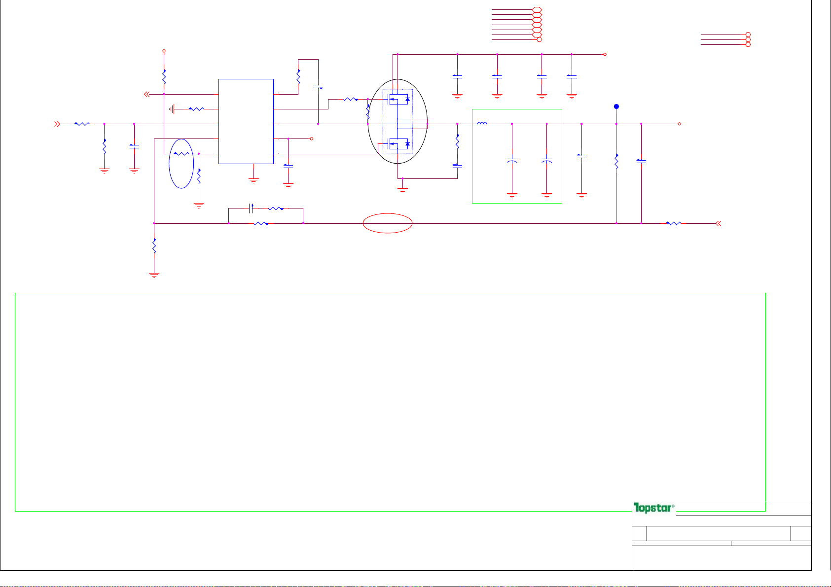
+VDC 24,37,39,40,44,47
+V3.3S 7,14,15,16,17,18,19,20,21,22,24,25,29,30,31,32,33,34,35,40,42,43,44,45,47
+V5S 15,16,22,24,25,27,28,29,30,40,42,44,45,47
+V1.05S 6,7,9,15,16,17,21,22,30,44,47
+V1.8S 10,20,21,40,45
+V3.3AL 7,15,16,17,19,20,22,24,28,31,33,40,43,45
+V3.3S
PU6
tps51218
PR215
47K
FCCM
模式
R0402
PR288
200K
R0402
ns
PR216
120K
R0402
V1.05S_PWG33,43
PR219
2K
R0402
V1_05S_ON33
PR221
100K
R0402
PC151
0.022uF/16V,X7R
C0402
ns
预留
0.7V
PR50
10K,1%
R0402
QFN10_0D5_0D8G
TPS51218
1
PGO OD
2
TRI P
3
EN
4
VFB
5
RF
PR222
200K
R0402
Set Fsw 340KHz
4700pF/25V,X7R
C0402
PC45
ns
VBS T
DRV H
V5I N
DRV L
GND
11
PR47
4.99K,1%
R0402
PR217
2.2
PC153
R0402
+V5AL
LG_1.05S
0.1uF/25V,X7R
C0603
PR225
R0603
3
PR227
0
10K
R0402
4
5
18-20A
4.3m ohm@4.5V/AOL1718
10
9
HV_HG_1.05S
8
HV_LL_1.05S
SW
7
6
PC40
4.7uf/10V
C0805
PR46 0
R0402
ns
PQ88
2
1
D1
G 1
S1
8
7
6
D2
G2
S2
9
CSD87352 2N 30V
SON8_1D27_1D6G
电压反馈线,避开干扰区走线。
R0805
PR65
2.2
PC51
0.1uF/25V,X7R
C0603
PL5
1
1.0uH/11A
LS2_6530
PC61
1000pF/50V,X7R
C0402
PC156
1000pF/50V,X7R
C0402
12
1
+
PC170
560uF/2.5V/7mohm
CAP6D3X7A
+V5AL 24,33,36,39,43,45,46,47
PC206
4.7uF/25V SAMSUNG
C0805
PC168
560uF/2.5V/7mohm
12
CAP6D3X7A
1
+
PC207
4.7uF/25V SAMSUNG
C0805
18-20A
PC155
C0402
0.1uF/10V,X7R
PR48
100
R0402
ns
+VDC
3A
V1_05S1
TestP
TPC60
ns
18-20A
PC50
C0402
0.1uF/10V,X7R
ns
PR49 10 R0402
VC CI O/ VC C_ PC H
IC Cm ax =2 0A
+/ -2 % DC ,
3% A C+ ri pp le
Sw it ch er
+V1.05S
VCCP_SENSE 9
AD+ 37,39
BATT+ 37,38
+V1.5 7,14,40,45
Del HM75 Option part.
TOPSTAR TECHNOLOGY
TOPSTAR TECHNOLOGY
TOPSTAR TECHNOLOGY
Page Name
Page Name
Page Name
Size
Size
Size
Project Name Rev
Project Name Rev
Project Name Rev
A3
A3
A3
Date: Sheet of
Date: Sheet of
Date: Sheet of
PROPERTY NOTE: this document contains information confidential and property to
PROPERTY NOTE: this document contains information confidential and property to
PROPERTY NOTE: this document contains information confidential and property to
TOPSTAR and shall not be reproduced or transferred to other documents or disclosed
TOPSTAR and shall not be reproduced or transferred to other documents or disclosed
TOPSTAR and shall not be reproduced or transferred to other documents or disclosed
to others or used for any purpose other than that for which it was obtained without
to others or used for any purpose other than that for which it was obtained without
to others or used for any purpose other than that for which it was obtained without
the expressed written consent of TOPSTAR
the expressed written consent of TOPSTAR
the expressed written consent of TOPSTAR
+V1.05S/+V1.8S
+V1.05S/+V1.8S
+V1.05S/+V1.8S
CL42 EVT
CL42 EVT
CL42 EVT
41 51Wednesday, January 09, 2013
41 51Wednesday, January 09, 2013
41 51Wednesday, January 09, 2013
A
A
A
Page 42

+V5S 15,16,22,24,25,27,28,29,30,40,44,45,47
+V3.3S 7,14,15,16,17,18,19,20,21,22,24,25,29,30,31,32,33,34,35,40,41,43,44,45,47
+VCCSA 10
+VDC 24,37,39,40,41,44,47
+V3.3AL 7,15,16,17,19,20,22,24,28,31,33,40,43,45
PC284
10uf/6.3V
C0805
10uf/6.3V
+V5S
PC285
C0805
10uf/6.3V
PC286
C0805
2A 2A
4.7uf/10V
VCCSA_PWG43
+V5S
PC282
C0805
PR360
R0402
0
19
20
21
PC293
C0402
0.1uF/10V,X7R
22
23
24
PC291
0.22uF/16V,X7R
C0603
GND_TPS51461
PR370
0
R0402
+V3.3S
R0402
PR357
100K
PC281
1uf/10V
C0402
17
18
V5FILT
V5DRV
PGND1
PGND2
PGND3
VIN1
PU10
TPS51463
QFNS24_0D5_1G
VIN2
VIN3
GND01VREF2COMP3SLEW4VOUT
PR367
0
R0402
PR368
10K
R0402
GND_TPS51461
16
PGOOD
0.01uF/25V,X7R
GND_TPS51461
PR371
0
R0402
PR372
0
1K
GND_TPS51461
12
11
10
9
8
7
GND_TPS51461
R0402
PC400
33pF/50V,NPO
C0402
PR363
0 R0402
PR364
2.2
R0805
ns
PR361
R0402
1K
15
VID014VID1
PR362
R0402
13
G1
EN
GND1
BST
SW0
SW1
SW2
SW3
SW4
MODE
6
PR366
R0402
ns
GND2
G2
0
5
PC292
C0402
VCCSA_SELECT1 10
VCCSA_SELECT0 10
PR358
2K
PR359
100K
R0402
PC283
0.1uF/25V,X7R
C0603
LL_VCCSA
PC289
1000pF/50V,X7R
C0402
ns
R0402
PL10
1
1.0uH/11A
LS2_6530
电压反馈线,避开干扰区走线。
注意IC散热。尽可能在每层铺大散热铜皮。
VID0 VID1 Vo
0 0 0.9V
0 1 0.8V
1 0 0.775V
1 1 0.75V
VCCSA_ON 33
6A
PC544
22uF/6.3V,X5R
C0805
PC543
22uF/6.3V,X5R
C0805
PC546
22uF/6.3V,X5R
C0805
PC545
22uF/6.3V,X5R
C0805
PC290
C0402
0.1uF/10V,X7R
VCCSA1
TestP
TPC60
ns
ns
PR365
100
R0402
PR369
0
R0402
PR384
10K
R0402
ns
GND_TPS51461
OCP>8A
5% DC+
AC
Switcher
+VCCSA
6A
VCCSA_SENSE 10
TOPSTAR TECHNOLOGY
TOPSTAR TECHNOLOGY
TOPSTAR TECHNOLOGY
Page Name
Page Name
Page Name
Size
Size
Size
Project Name Rev
Project Name Rev
Project Name Rev
B
B
B
Date: Sheet of
Date: Sheet of
Date: Sheet of
PROPERTY NOTE: this document contains information confidential and property to
PROPERTY NOTE: this document contains information confidential and property to
PROPERTY NOTE: this document contains information confidential and property to
TOPSTAR and shall not be reproduced or transferred to other documents or disclosed
TOPSTAR and shall not be reproduced or transferred to other documents or disclosed
TOPSTAR and shall not be reproduced or transferred to other documents or disclosed
to others or used for any purpose other than that for which it was obtained without
to others or used for any purpose other than that for which it was obtained without
to others or used for any purpose other than that for which it was obtained without
the expressed written consent of TOPSTAR
the expressed written consent of TOPSTAR
the expressed written consent of TOPSTAR
+VCCSA
+VCCSA
+VCCSA
CL42 EVT
CL42 EVT
CL42 EVT
42 51Wednesday, January 09, 2013
42 51Wednesday, January 09, 2013
42 51Wednesday, January 09, 2013
A
A
A
Page 43
Power Good Logic CIRCUIT
+V3.3S
PR106
10K
R0402
+V3.3S 7,14,15,16,17,18,19,20,21,22,24,25,29,30,31,32,33,34,35,40,41,42,44,45,47
+V5AL 24,33,36,39,41,45,46,47
+V3.3AL 7,15,16,17,19,20,22,24,28,31,33,40,45
HV_SHDN#37
RESET_SW
BUTTON4A_5D0
Switch
112
334
2
4
MAIN_PWROK
TestP
V1.05S_PWG33,41
DDR_PWG40
VCCSA_PWG42
V1.8S_PWG40
PM_RSMRST#17,33
R290 1K
PM_SLP_S3#17,33
R0402
1
2
1
2
1
2
C196
0.1UF/10V,X7R
C0402
3
PD7
LRC 30V 200mA 5ns
SOT23
3
PD6
LRC 30V 200mA 5ns
SOT23
3
PD9
LRC 30V 200mA 5ns
SOT23
TPC60
ns
MAIN_PWROK 7,17,33
LM3Z5V6T1G 5.6V 5mA
+V5AL
+V3.3AL
LM3Z3V6T/3.6V/5mA
PZ6
SOD323
PZ12
SOD323
12
12
SHDN_LOCK#30
PR246
10
R0402
PR142 0
R0402
PQ48
LMBT3904LT1G
SOT23
1
PC107
1uf/10V
C0402
Page Name
Page Name
Page Name
Size
Size
Size
A4
A4
A4
Date: Sheet of
Date: Sheet of
Date: Sheet of
PROPERTY NOTE: this document contains information confidential and property to
PROPERTY NOTE: this document contains information confidential and property to
PROPERTY NOTE: this document contains information confidential and property to
TOPSTAR and shall not be reproduced or transferred to other documents or disclosed
TOPSTAR and shall not be reproduced or transferred to other documents or disclosed
TOPSTAR and shall not be reproduced or transferred to other documents or disclosed
to others or used for any purpose other than that for which it was obtained without
to others or used for any purpose other than that for which it was obtained without
to others or used for any purpose other than that for which it was obtained without
the expressed written consent of TOPSTAR
the expressed written consent of TOPSTAR
the expressed written consent of TOPSTAR
PR139
100
R0402
Project Name Rev
Project Name Rev
Project Name Rev
2 3
PR146
100
R0402
PQ49
LMBT3904LT1G
SOT23
1
2 3
PR143
20K
R0402
TOPSTAR TECHNOLOGY
TOPSTAR TECHNOLOGY
TOPSTAR TECHNOLOGY
Power Good Logic/OVP
Power Good Logic/OVP
Power Good Logic/OVP
CL42 EVT
CL42 EVT
CL42 EVT
PR147
51K
R0402
1
PQ44
23
LMBT2907ALT1G
SOT23
PC108
0.22uF/16V,X7R
C0603
43 51Wednesday, January 09, 2013
43 51Wednesday, January 09, 2013
43 51Wednesday, January 09, 2013
A
A
A
Page 44

5
VGFXVSSSEN10
PC534
0.01uF/16V,X7R
PR435
R0402
2K
PR456
3.24K,1%
R0402
for LL.
-2.9mohm
R0402
+V3.3S
6.98K,1%
C0402
PC535
330pF/50V,X7R
ns
C0402
for LL.
-4.6mohm GT1
-3.9mohm GT2
PR428
3.01K,1%
R0402
33pF/50V,NPO
PC375
C0402
1000pF/50V,X7R
DATA1
CLK1
IMVPON1
ns
VCORE_POK
ns
ns
ICTP
ns
PR454
R0402
PC385
470pF/25V,X7R
C0402
PR457
422K OHM 1%
R0402
R808
0
R0402
GND_CORE
PC369
C0402
PR434
6.98K,1%
R0402
10
G1
G2
PC382
1000pF/50V,X7R
C0402
R809
1.87K,1%
R0402
PR473
2.37K,1%
R0402
PR470
100,1%
R0402
PC368
470pF/25V,X7R
C0402
PR429
294K 1%
R0402
40
1
VWG
COMPG
2
PGOODG
3
SDA
4
ALERT#
5
SCLK
ICTP
6
VR_ON
ICTP
7
ICTP
PGOOD
8
VR_HOT#
9
NTC
VW
G1
COMP11FB12NC113NC214NC315RTN16ISUMN17ISUMP18VDD19VIN
G2
G3G3G4
G4
PC392
33pF/50V,NPO
C0402
PR462
604,1%
R0402
PC397
470pF/25V,X7R
C0402
PC536
330pF/50V,X7R
ns
C0402
PC537
0.01uF/16V,X7R
C0402
D D
C C
+V1.05S
VR_SVID_DATA9
VR_SVID_ALERT#9
VR_SVID_CLK9
IMVP_PWRGD33
VR_PROCHOT#7
B B
A A
PR442 0
PR443 0
PR444 0
IMVP_ON33
R0402
R0402
R0402
GND_CORE
PR438
130,1%
R0402
PR439
54.9,1%
R0402
NTC
thermi stor放到
板面最热的地方
5
GND_CORE
GND_CORE
PR440
100
R0402
PR451
4.02K,1%
R0402
VCCSENSE9
VSSSENSE9
VGFXVCCSEN10
+V3.3S
GND_CORE
GND_CORE
PC367
470pF/25V,X7R
C0402
PR432 169K,1%
GFX_POK
ICTP
ns
PR445 1K R0402
PR446 2K R0402
PR449 28K,1% R0402
PR452 470K,1% R0603
PC359
470pF/25V,X7R
C0402
PR474
511,1%
R0402
39
FBG
PR463
R0402
GND_CORE
37
38
RTNG
T88
ns
2K
PC398
1000pF/50V,X7R
C0402
4
PC538
270pF/50V,X7R
C0402
ns
PR419 1.37K,1% R0402
PC371
0.22uF/16V,X7R
C0603
PR433
2.2
R0603
ntcg
35
36
NTCG
ISUMPG
ISUMNG
PU12
ISL95837 SVID
QFNS40_0D4_1G
ICTP
4
3
PR471
100
R0402
ns
PC540
PC541
0.1uF/10V,X7R
0.1uF/10V,X7R
C0402
C0402
PQ86
CSD87352 2N 30V
SON8_1D27_1D6G
PR426
0
R0603
HV_HG_GFX
HV_LL_GFX
32
33
34
BOOTG
PHASEG
UGATEG
PC393
680pF/25V,X7R
C0402
ns
HV_LG_GFX
31
LGATEG
LGATE
PHASE
UGATE
20
PC384
1uF/10V,X7R
C0603
PR466
1.33K,1%
R0402
GND_CORE
PR427
10K
R0402
NC8
NC7
NC6
NC5
VCCP
NC4
BOOT
G9
G8
G5G5G6
G7
G6
PR458
1 R0402
PR464
100
R0402 ns
0PR430 R0603
3
G1
4
5
G2
30
29
28
27
26
25
24
23
22
21
G9
G8
G7
PC383
0.1uF/25V,X7R
C0603
0PR467 R0603
0.047uF/16V,X7R
1000pF/50V,X7R
2
1
D1
S1
D2
S2
9
T87
HV_LG_CPU
HV_LL_CPU
ns
HV_HG_CPU
PR469
2.2 R0603
+VDC
GND_CORE
+V5S
PC395
0.22uF/10V,X7R
C0402
PC356
C0402
ns
PC357
C0402
8
7
6
PR431
2.2
R0805
PC374
1000pF/50V,X7R
C0402
GND_CORE
PC376
1uF/10V,X7R
C0603
ICTP
PC379
0.22uF/16V,X7R
C0603
GND_CORE
PC539
0.1uF/10V,X7R
C0402
PC542
0.1uF/25V,X7R
C0603
PC394
0.01uF/25V,X7R
C0402
ns
PR421
11K,1%
R0402
PC361
4.7uF/25V SAMSUNG
C0805
NTC
thermi stor放到
板面最热的地方
+V5S
0PR448 R0603
PR450
10K
R0402
0PR453 R0603
1000pF/50V,X7R
PC396
0.047uF/16V,X7R
C0402
ns
NTC
PR420
10K,1%
R0603
PR422
2.61K,1%
R0402
PR472 1.87K,1%R0402
PC358
4.7uF/25V SAMSUNG
C0805
2A
PR436
4.02K,1%
R0402
5
4
G1
3
3A
PC386
C0402
3
+VDC
Co-lay
PL9
1.0uH/11A
LS2_6530
ns
PR437 28K,1% R0402
PR441 470K,1% R0603
PQ16
9
S2
G2
D2
6
7
8
S1
D1
2
1
CSD87351 2N 30V
SON8_1D27_1D6G
PC388
0.1uF/25V,X7R
C0603
PC387
0.01uF/25V,X7R
C0402
PR460
11K,1%
R0402
PL17
0.36uH/30A
ls2_1040
1
1
PC390
4.7uF/25V SAMSUNG
C0805
PC389
4.7uF/25V SAMSUNG
C0805
ISUMP
PR461
2.61K,1%
R0402
NTC
PR465
10K,1%
R0603
ISUMN
PC399
0.1uF/10V,X7R
C0402
GND_CORE
+VCC_GFX
ntcg
PC377
1000pF/50V,X7R
C0402
PR447
2.2
R0805
PR459 1.87K,1%R0402
PC72
560uF/2.5V/7mohm
CAP6D3X7A
+VDC
1
12
+
12
1
+
PC73
560uF/2.5V/7mohm
CAP6D3X7A
PL4
0.36uH/30A
ls2_1040
1
PC208
330uF/2.5V
CT7343_19
PR455
10
R0402
2
12
1
PC373
+
C0402
0.1uF/10V,X7R
ns
12
1
+
PC70
560uF/2.5V/7mohm
CAP6D3X7A
2
VGFX1
TestP
TPC60
ns
12A
12
1
+
330uF/2.5V
CT7343_19
PC71
560uF/2.5V/7mohm
CAP6D3X7A
CPU端加12×10uF MLCC
+V3.3S 7,14,15,16,17,18,19,20,21,22,24,25,29,30,31,32,33,34,35,40,41,42,43,45,47
+V5S 15,16,22,24,25,27,28,29,30,40,42,45,47
+VDC 24,37,39,40,41,47
+VCC_CORE 9
+V1.05S 6,7,9,15,16,17,21,22,30,41,47
+VGFX 10
+VGFX
ITDP :12 A
Iccm ax: 18A GT 1
ITDP :18 .3A
Iccm ax: 29A GT 2
CPU端加10×10uF MLCC
25A
VCORE1
TestP
LL=- 2.9
TPC60
ns
mOhm
+VCC_CORE
12
1
PC381
PC67
+
C0402
0.1uF/10V,X7R
ns
ITDP :25 A
Iccm ax: 33 A
Page Name
Page Name
Page Name
Size
Size
Size
Project Name Rev
Project Name Rev
Project Name Rev
A2
A2
A2
Date: Sheet of
Date: Sheet of
Date: Sheet of
PROPERTY NOTE: this document contains information confidential and property to
PROPERTY NOTE: this document contains information confidential and property to
PROPERTY NOTE: this document contains information confidential and property to
TOPSTAR and shall not be reproduced or transferred to other documents or disclosed
TOPSTAR and shall not be reproduced or transferred to other documents or disclosed
TOPSTAR and shall not be reproduced or transferred to other documents or disclosed
to others or used for any purpose other than that for which it was obtained without
to others or used for any purpose other than that for which it was obtained without
to others or used for any purpose other than that for which it was obtained without
the expressed written consent of TOPSTAR
the expressed written consent of TOPSTAR
the expressed written consent of TOPSTAR
1
TOPSTAR TECHNOLOGY
TOPSTAR TECHNOLOGY
TOPSTAR TECHNOLOGY
Robin
Robin
Robin
+VCC_CORE/+VFX
+VCC_CORE/+VFX
+VCC_CORE/+VFX
CL42 EVT
CL42 EVT
CL42 EVT
1
A
A
A
44 51Wednesday, January 09, 2013
44 51Wednesday, January 09, 2013
44 51Wednesday, January 09, 2013
Page 45

5
+12V
2 3
PC199
c0402
ns
LDTB114ELT1G
SOT23
1
PQ58
+12V
1
PQ73
L2N7002LT1G
SOT23
PR224
10K
R0402
0.01uF/25V,X7R
PR269
120K
R0402
3
2
D D
MAIN_OFF
MAIN_ON
C C
B B
A A
PR148
1K
R0402
PM_SLP_SUS#17,33,39
ALWAYS_ON33,39,46
VerC: add SLP_SUS# to DS3 power
Swain 111206
DS3
PR273
1K
R0402
noDS3
PR152
510K
R0402
1
1KPR274 R0402
5
PR228
100K
R0402
PR229
1K
R0402
3
2
PQ72
L2N7002LT1G
SOT23
1
PR276
510K
R0402
PQ52
L2N7002LT1G
SOT23
EC_RTC
PR270
51K
R0402
3
2
PC165
0.01uF/25V,X7R
C0402
PR286
1K
R0402
0.01uF/25V,X7R
4
+V5S 15,16,22,24,25,27,28,29,30,40,42,44,47
+V3.3S 7,14,15,16,17,18,19,20,21,22,24,25,29,30,31,32,33,34,35,40,41,42,43,44,47
+V5AL 24,33,36,39,41,43,46,47
+V1.5 7,14,40
+12V 24,27,39,46
HV_SPower_Driver
+V5AL
PR223
33K
R0402
PC159
C0402
PR275
1M
R0402
4
HV_APower_Driver
4
3A
PQ56
56789
AON7410
D
G
PC154
1uf/10V
C0402
SO8_26_130
S
123
LRC LMDL914T1G 100V 200mA
PD16
SOD323
1
PR265
300K
R0402
V5S1
TestP
TPC60
ns
+V5S
3A
PC191
0.01uF/25V,X7R
C0402
100KPR264
R0402
PC180
0.01uF/25V,X7R
C0402
56789
D
4
G
S
+V3.3SB
123
1
PR24
20K
R0402
5A
PQ23
AON7410
SO8_26_130
PC28
C0402
1uf/10V
+V5AL
3
2
PR135
10K
R0402
1mA
PQ75
L2N7002LT1G
SOT23
PC190
1uf/10V
C0402
3
PD2
LRC LMDL914T1G 100V 200mA
SOD323
1
PR25
51K
R0402
PC23
0.01uF/25V,X7R
C0402
PD10
LRC LMDL914T1G 100V 200mA
SOD323
PR130
100K
R0402
V3_3AL1
TestP
TPC60
ns
+V5AL_PCH
1mA
3
4
G
1
PR134
100K
R0402
PC100
0.01uF/25V,X7R
C0402
+V3.3AL
5A
+V3.3AL
56789
D
S
SO8_26_130
dri1.5
3A
123
PC17
C0402
1uf/10V
PQ42
AON7410
4
PR144
100
R0402
PQ13
AON7410
SO8_26_130
56789
D
G
S
+V1.5S
1 2
3
2
V3_3S1
TestP
TPC60
ns
+V1.5
2A
dri1.5
123
PC101
1uf/10V
C0402
PR141
100
R0402
ns
PQ46
L2N7002LT1G
SOT23
1
4
+V3.3S
3A
56789
D
G
S
PQ45
L2N7002LT1G
SOT23
2
1
MAIN_OFF
2
ns
123
PR140
100
R0402
ns
PQ43
AON7410
SO8_26_130
ns
PR150
100
R0402
3
2
1
+V1.8S 10,20,21,40
+V0.75S 14,40
+V1.5S 7,10,21,31
+V3.3SB 7,15,17,20,22,28,31,33,35,37,38,39
+V5AL_PCH 22
+V3.3AL 7,15,16,17,19,20,22,24,28,31,33,40,43
EC_RTC 15,27,39
+V1.5
PR115
100
R0402
ns
+V1.5S
PM_SLP_S4#33,39
V1_5S1
TestP
TPC60
ns
VDDRDISCHG
PR128
10K
R0402
ns
PQ35
L2N7002LT1G
SOT23
1
ns
1 2
3
2
PQ34
L2N7002LT1G
SOT23
ns
1
VDDRDISCHG
3
2
2A
PQ47
L2N7002LT1G
SOT23
1
+V0.75S
PR145
47
R0402
3
2
TOPSTAR TECHNOLOGY
TOPSTAR TECHNOLOGY
TOPSTAR TECHNOLOGY
SYSTEM/DISCHARGE
SYSTEM/DISCHARGE
SYSTEM/DISCHARGE
CL42 EVT
CL42 EVT
CL42 EVT
1
PR151
100
R0402
PQ51
L2N7002LT1G
SOT23
1
45 51Wednesday, January 09, 2013
45 51Wednesday, January 09, 2013
45 51Wednesday, January 09, 2013
+V3.3S+V5S
PR149
100
R0402
1 2
1 2
PQ89
3
L2N7002LT1G
SOT23
1
2
Page Name
Page Name
Page Name
Size
Size
Size
Project Name Rev
Project Name Rev
Project Name Rev
A3
A3
A3
Date: Sheet of
Date: Sheet of
Date: Sheet of
PROPERTY NOTE: this document contains information confidential and property to
PROPERTY NOTE: this document contains information confidential and property to
PROPERTY NOTE: this document contains information confidential and property to
TOPSTAR and shall not be reproduced or transferred to other documents or disclosed
TOPSTAR and shall not be reproduced or transferred to other documents or disclosed
TOPSTAR and shall not be reproduced or transferred to other documents or disclosed
to others or used for any purpose other than that for which it was obtained without
to others or used for any purpose other than that for which it was obtained without
to others or used for any purpose other than that for which it was obtained without
the expressed written consent of TOPSTAR
the expressed written consent of TOPSTAR
the expressed written consent of TOPSTAR
+V1.8S
1 2
3
2
+12V
PR127
510K
R0402
ns
PR110
510K
R0402
ns
A
A
A
Page 46

5
4
3
2
1
+V5AL 24,33,36,39,41,43,45,47
+12V 24,27,39,45
D D
7V_LED_Panel(min)
7V_LED_Panel(min)
PL15
10uH/0.7A
LS2_3513
PD27 SSM34PT
+V5AL +12V
1
1
SMA
PC410
10uF/16V X5R
C1206
7V_LED_Panel(min)
PC423
10uF/16V X5R
C1206
7V_LED_Panel(min)
PC184
10uF/6.3V,X5R
C0805
C C
7V_LED_Panel(min)
7V_LED_Panel(min) PR59
PR56
HV_LL_+V12AL
0
R0402
freq=1.2MHz for Freq=5V;
PR55
0
R0402
ns
PC169
C0402
0.022uF/16V,X7R
PU13
RT9277B
MSOP8_0D65_1D1
5
LX
6
VIN
7
FREQ
8
SS
7V_LED_Panel(min)
GND
EN
FB
COMP
PR54
4
0
R0402
3
7V_LED_Panel(min)
Vref=1.24Vfreq=640KHz for Freq=0V;
2
1
PC171
C0402
22pF/50V,NPO
7V_LED_Panel(min)
ALWAYS_ON 33,39,45
7V_LED_Panel(min)
PR57
100K
R0402
PC411
33uF/25V
CAP6_6x7_3
12
1
+
7V_LED_Panel(min)
PC189
C0402
1000pF/50V,X7R
7V_LED_Panel(min)
300mA max
I rush=1A
80.6K,1%
R0402
7V_LED_Panel(min)
PR58
9.31K,1%
R0402
7V_LED_Panel(min)
7V_LED_Panel(min)
B B
Reserve for 7V LED Panel, Defaut ns.
If use, PR55 no stuff
TOPSTAR TECHNOLOGY
TOPSTAR TECHNOLOGY
TOPSTAR TECHNOLOGY
Robin
Robin
Robin
Page Name
Page Name
Page Name
Size
Size
A A
5
4
3
Size
Project Name Rev
Project Name Rev
Project Name Rev
A
A
A
Date: Sheet of
Date: Sheet of
Date: Sheet of
PROPERT Y NOTE: this document contains information confidential and property to
PROPERT Y NOTE: this document contains information confidential and property to
PROPERT Y NOTE: this document contains information confidential and property to
TOPSTAR and shall not be reproduced or transferred to other documents or disclosed
TOPSTAR and shall not be reproduced or transferred to other documents or disclosed
TOPSTAR and shall not be reproduced or transferred to other documents or disclosed
to others or used for any purpose other than that for which it was obtained without
to others or used for any purpose other than that for which it was obtained without
to others or used for any purpose other than that for which it was obtained without
the expressed written consent of TOPSTAR
the expressed written consent of TOPSTAR
the expressed written consent of TOPSTAR
2
Blank
Blank
Blank
TU142 PVT
TU142 PVT
TU142 PVT
C
C
C
46 51Wednesday, January 09, 2013
46 51Wednesday, January 09, 2013
46 51Wednesday, January 09, 2013
1
Page 47

5
4
3
2
+V3.3S 7,14,15,16,17,18,19,20,21,22,24,25,29,30,31,32,33,34,35,40,41,42,43,44,45
+V5AL 24,33,36,39,41,43,45,46
+VDC 24,37,39,40,41,44
+V5S 15,16,22,24,25,27,28,29,30,40,42,44,45
+V1.05S 6,7,9,15,16,17,21,22,30,41,44
+VCCSA 10,42
1
FD1
D D
+VDC
+V5S
+V1.05S
PC425
0.1uF/25V,X7R
C0603 C268
C C
PC424
0.1uF/25V,X7R
C0603
+VDC
PC7
0.1uF/25V,X7R
C0603
+V5S + V5S
C283
0.1UF/10V,X7R
C0402
+V3.3S+V3.3S
+V1.05S +V5AL
C289
0.1UF/10V,X7R
C0402
C271
0.1UF/10V,X7R
C0402
+V5S
C284
0.1UF/10V,X7R
C0402
C299
0.1UF/10V,X7R
C0402
+V5AL
+V5AL
+V5S
C539
0.1UF/10V,X7R
C0402
0.1UF/10V,X7R
C0402
H1
C257
0.1UF/10V,X7R
C0402
+V1.05S
C285
0.1UF/10V,X7R
C0402
+V5S
0.1UF/10V,X7R
C0402
H2
+V3.3S
C258
C265
0.1UF/10V,X7R
C0402
0320:Del NUT3,SU341 H3 cut half.
H3
H4
NUT5
D_BOT
H5
FMARKS
ns
FMARKS
FD6
FMARKS
ns
FMARKS
FD11
FMARKS
ns
FMARKC
1
1
1
H8
FD2
1
FMARKS
ns
FMARKS
FD7
1
FMARKS
ns
FMARKS
FD12
1
FMARKS
ns
FMARKC
FD3
FD4
FD5
1
1
1
FMARKS
ns
FMARKS
FD8
1
1
FMARKS
ns
FMARKS
FD13
1
1
FMARKS
ns
FMARKC
1
1
FMARKS
ns
FMARKS
FD9
1
1
FMARKS
ns
FMARKS
FD14
1
1
FMARKS
ns
FMARKC
H9
1
1
1
FMARKS
ns
FMARKS
FD10
1
1
1
1
FMARKS
ns
FMARKS
FD15
FD16
1
1
FMARKS
ns
FMARKC
H11
1
1
H12
1
1
FMARKS
ns
FMARKC
HOLE
1
TH_256_138
ns
HOLE
1
TH_256_138
ns
2
HOLE
1
TH_256_100A
ns
HOLE
1
TH_236_100
ns
H6
HOLE
1
TH_256_138
ns
Page Name
Page Name
Page Name
Size
Size
Size
A3
A3
A3
Date: Sheet of
Date: Sheet of
Date: Sheet of
PROPERTY NOTE: this document contains information confidential and property to
PROPERTY NOTE: this document contains information confidential and property to
PROPERTY NOTE: this document contains information confidential and property to
TOPSTAR and shall not be reproduced or transferred to other documents or disclosed
TOPSTAR and shall not be reproduced or transferred to other documents or disclosed
TOPSTAR and shall not be reproduced or transferred to other documents or disclosed
to others or used for any purpose other than that for which it was obtained without
to others or used for any purpose other than that for which it was obtained without
to others or used for any purpose other than that for which it was obtained without
the expressed written consent of TOPSTAR
the expressed written consent of TOPSTAR
the expressed written consent of TOPSTAR
HOLE
1
TH_236_100
ns
Project Name Rev
Project Name Rev
Project Name Rev
HOLE
1
TH_256_138
B B
A A
5
4
ns
HOLE
1
TH_236_100
ns
3
HOLE
1
TH_256_100A
ns
NUT7
D_BOT
HOLE
1
TH_236_100
ns
H7
HOLE
1
TH_256_138
ns
TOPSTAR TECHNOLOGY
TOPSTAR TECHNOLOGY
TOPSTAR TECHNOLOGY
Robin
Robin
Robin
Hole&Stiching Cap
Hole&Stiching Cap
Hole&Stiching Cap
TU142 PVT
TU142 PVT
TU142 PVT
1
C
C
47 51Sunday, April 07, 2013
47 51Sunday, April 07, 2013
47 51Sunday, April 07, 2013
C
Page 48
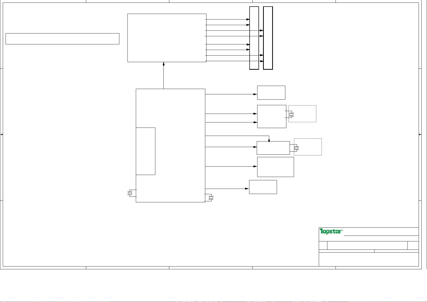
5
D D
CLOCK Distribution:
4
Ivy Bridge
BCLK_CPU
3
M_CLK_DDR0
M_CLK_DDR#0
M_CLK_DDR2
M_CLK_DDR#2
M_CLK_DDR1
M_CLK_DDR#1
M_CLK_DDR3
M_CLK_DDR#3
2
SODIMM0
SODIMM1
1
100 MHz
CLK_OUT_DMI_N
CLK_OUT_DMI_P
C C
PCIE 100MHz
PCIE 100MHz
Panther Point
LAN Chip 25M
Mini PCIE
PCIE LAN
25MHz
Reserved
32.768MHz
33MHz
B B
PCIE clock
48MHz
24MHz
32.768KHz
A A
5
4
25MHz
3
EC(KB3930)
Card Reader
(IT1337E)
Audio Codec
ALC662
32.768KHz
Reserved
2
Topstardigital
Topstardigital
Topstardigital
连子键
连子键
Page Name
Page Name
Page Name
Size
Size
Size
Project Name Rev
Project Name Rev
Project Name Rev
B
B
B
Date: Sheet of
Date: Sheet of
Date: Sheet of
PROPERTY NOTE: this document contains information confidential and property to
PROPERTY NOTE: this document contains information confidential and property to
PROPERTY NOTE: this document contains information confidential and property to
TOPSTAR and shall not be reproduced or transferred to other documents or disclosed
TOPSTAR and shall not be reproduced or transferred to other documents or disclosed
TOPSTAR and shall not be reproduced or transferred to other documents or disclosed
to others or used for any purpose other than that for which it was obtained with the
to others or used for any purpose other than that for which it was obtained with the
to others or used for any purpose other than that for which it was obtained with the
expressed written consent of TOPSTAR
expressed written consent of TOPSTAR
expressed written consent of TOPSTAR
连子键
Clock Distribution
Clock Distribution
Clock Distribution
CL42 EVT
CL42 EVT
CL42 EVT
48 51Wednesday, January 09, 2013
48 51Wednesday, January 09, 2013
48 51Wednesday, January 09, 2013
1
A
A
A
Page 49

5
Power On Sequence(Battery mode)
G3
With Main Battery
Without AC adapter
CPURST#
PCIRST#
SUS_STAT#
(CPU PWRGD)
D D
+V3.3S,+V5S,+V1.5S,+V1.05S,+V1.8,
+V1.8S,+V0.9S,+V0.89S
V0_9S_ON,V1_8S_ON V1_05S_ON,V0_89S_ON(EC Output)
H_PWRGD
PM_ICH_PWROK (Input to ICH)
Clock Gen Output
IMVP_PWRGD
CK505_CLK_EN#
+VCC_CORE
IMVP_ON(EC Output)
MAIN_PWROK(Input to EC)
V1_8_ON(EC Output)
MAIN_ON(EC Output)
SLP_S3#(Input to EC)
SLP_S4#(Input to EC)
PWRBTN#(EC Output)
ALWAYS_ON(EC Output)
C C
RSMRST#(Input to EC)
+V3.3AL,+V5AL
PWRSW#(Input to EC)
(PRESS POWER BUTTON)
EC_RTC
+VDC
RTCRST#
VCCRTC
S0
SUS_STAT#
STP_PCI#
PCIRST#
PLTRST#
SLP_S3#(Input to EC)
SLP_S4#(Input to EC)
IMVP_ON(EC Output)
IMVP_PWROK(ISL6545 Output)
MAIN_PWROK
B B
V0_9S_ON,V1_8S_ON V1_05S_ON,V0_89S_ON(EC Output)
+V3.3S,+V5S,+V2.5S,+V1.5S,+V1.05S,+V1.8,
+V1.8S,+V0.9S,+V0.89S
MAIN_ON(EC Output)
V1_8_ON(EC Output)
ALWAYS_ON(EC Output)
+V3.3AL,+V5AL
RSMRST#(Input to EC)
IacN
T04
T04
T03
Press Power Button
T01
T02
Power Off Sequence(Battery Mode)
S0
T18
T21
T19
T22
T22a
S5G3
T06
S5
T22c
Pull out
Main
Battery
130ms
PLUG
Main
Battery
S5
T49
Keep up
+V3.3AL
S3/S4/S5
T08
T23
T10
G3
4
3
2
1
Power On Sequence(Adapter mode)
G3
S0
T24
T14
S0
T16
T15
T17
PM_ICH_PWROK (Input to ICH)
MAIN_PWROK(Input to EC)
+V3.3S,+V5S,+V2.5S,+V1.5S,+V1.05S,+V1.8,
+V1.8S,+V0.9S,+V0.89S
V0_9S_ON,V1_8S_ON V1_05S_ON,V0_89S_ON(EC Output)
ALWAYS_ON(EC Output)
SLP_S3#(Input to EC)
SLP_S4#(Input to EC)
PWRSW#(Input to EC)
RSMRST#(Input to ICH&EC)
+V3.3AL,+V5AL,
+V5_STBY,EC_RTC
CPURST#
PCIRST#
PLTRST#
SUS_STAT#
(CPU PWRGD)
H_PWRGD
Clock Gen Output
IMVP_PWRGD
CK410_CLK_EN#
+VCC_CORE
IMVP_ON(EC Output)
V1_8_ON(EC Output)
MAIN_ON(EC Output)
PWRBTN#(EC Output)
(PRESS POWER
PWRSWVCC2
BUTTON)
RTCRST#
VCCRTC
With AC adapter
AC_IN
+VDC
G3
T04
T04
T03
T01
T02
S5
T06
S3/S4/S5
130ms
T49
Press Power Button
S0
T24
T14
T23
T10
T08
PLUG
Adapter
S0
T16
T15
T17
MAIN_PWROK(Input to EC)
+V0.89S
+V1.8S
CHIPPWROK
+V1.05S
+V1.5S
+V0.9S
+V3.3S,+V5S
+V1.8
V0_9S_ON,V1_8S_ON V1_05S_ON,V0_89S_ON(EC Output)
电源控制信号时序
+V1.8 V1 _8_ON EC
+V0.9 V0 _9S_ON EC
+V1.5S V1_5S_ON SLP_S3
+V5S MA IN_ON EC
+V3.3S M AIN_ON EC
+0.89S V0_89S_ ON V1_05S_ON
+1.05S V1_05S_ ON V1_5_ON
+1.8S V1.8S_ON(+1. 05SPWROK) V1_ 05S_ON
才能发
V1.8S_ON
DESIGN NOTE
THIS CIRCU IT ENSURES
+1.8S COME UP A FTER +1.05S
+1.05S COME UP AFTER +1.5S
收到
收到
高电平信号
收到
收到
SLP_S4
SLP_S3
信号变高
SLP_S3
SLP_S3
信号变高,发出
信号变高,发出
2MS
信号变高,发出
信号变高,发出
变高
2MS后,
变高
2MS后,
后,才能发
才能发
才能发
变高
V1_8_ON
V0_9S_ON
V1_5_ON
MAIN_ON
MAIN_ON
V0_89S_ON
V1_05_ON
2MS后 ,
高电平。
高电平。
高电平信号
高电平。
高电平。
高电平信号
高电平信号
Power Off Sequence(Adapter Mode)
SUS_STAT#
STP_PCI#
PCIRST#
PLTRST#
SLP_S3#(Input to EC)
SLP_S4#(Input to EC)
IMVP_ON(EC Output)
IMVP_PWROK(ISL6545 Output)
MAIN_PWROK
MAIN_ON(EC Output)
V0_9S_ON(EC Output)
+V3.3S,+V5S,+V2.5S,+V1.5S,+V1.05S,+V1.8,
+V0.9S
V1_8_ON(EC Output)
ALWAYS_ON(EC Output)
IacN
ACIN
+V3.3AL
+V5AL
S0
S5
S0
T18
T21
T19
S5
T22
T22a
Pull out
AC_ADPTER
G3
A A
Topstardigital
Topstardigital
Topstardigital
连子键
连子键
1
连子键
Power On/OFF
Power On/OFF
Power On/OFF
CL42 EVT
CL42 EVT
CL42 EVT
A
A
A
49 51Wednesday, January 09, 2013
49 51Wednesday, January 09, 2013
49 51Wednesday, January 09, 2013
Page Name
Page Name
Page Name
Size
Size
Size
Project Name Rev
Project Name Rev
Project Name Rev
A2
A2
A2
Date: Sheet of
Date: Sheet of
Date: Sheet of
PROPERTY NOTE: this document contains information confidential and property to
PROPERTY NOTE: this document contains information confidential and property to
PROPERTY NOTE: this document contains information confidential and property to
TOPSTAR and shall not be reproduced or transferred to other documents or disclosed
TOPSTAR and shall not be reproduced or transferred to other documents or disclosed
TOPSTAR and shall not be reproduced or transferred to other documents or disclosed
to others or used for any purpose other than that for which it was obtained with the
to others or used for any purpose other than that for which it was obtained with the
to others or used for any purpose other than that for which it was obtained with the
expressed written consent of TOPSTAR
expressed written consent of TOPSTAR
5
4
3
2
expressed written consent of TOPSTAR
Page 50
5
4
3
2
1
1B
D D
1A
AD+
PD1
PQ2
PQ1
+VDC
BATT+
Always_On
Power
RT8205
PWRSWVCC2
ALWAYS_ON
5A
3B
AD+
C C
PWRSWVCC2
TigerPoint
ICH_POWGD
PLT_RST#
21
B B
H_PWRGD
22
22
ALW_EN
ALW_PWROK
PM_SLP_S4#
PM_SLP_S3#
VR_PWRGD_EN
19
7
7
PWRSW#
7B
PM_RSMRST#
PM_PWRBTN#
+V1.05S
+VCCSA
DDR POWER
3A
TPS51218
10
V1_5_ON
6A
5B
8
8
4A 6B
EC_KBC
KB3930
V1_5S_ON
7
ALWAYS_ON
VCCSA_ON
V1_05S_ON
13
12
TPS51218
+V1.05S Power
TPS51218
+VCCSA Power
2A
ALW_PWROK
3A
V1_5_PWROK
DDR_PWROK
V0_75S_ON
IMVP_ON
17
2B
5B
4B
2A
11
11
11
10
MAIN_ON
SET_I
CHG_ON
SYS_I_Sense
MAIN_PWROK
to IMVP_ON
Delay 100mS
+V5_STBY
EC_RTC
+V3.3AL
+V5AL
+V1.5
APL5331
MAIN_PWROK
V1_5S_ON
+V3.3S
MAIN_ON
16
13
9
+V0.75S
PU7
APL5331
+V1.8
V1_05S PG
System Power
+V_S
DDR_PWG
DDR_PWG
CHIPPWROK
PM_RSMRST#
PM_SLP_S3#
V1_05S
+V1.5S
14
+V1.5S
14
15
5A 6B
8
CHIPPWROK
+V1.5S
+V1.8S
+V3.3S
+V5S
14
15
+VDC
SYS_I_Sense
SET_I
CHG_ON
Charge
ISL6251
AC_IN
BATT+
Note:
*A:For adapter in
IMVP_ON
17
20
IMVP_PWRGD
PineViwe
H_PWRGD
A A
+VCC_CORE
18
VCC_CORE
TPS51218
+VCC_CORE
VR_PWRGD_CLK_EN
19
VR_PWRGD
CLK_EN
MAIN_PWROK
20
Clock
CK410M
IMVP_PWRGD
19
19
ICH_POWGD
21
CPU
5
4
3
2
*B:For battery only
* :For all
Page Name
Page Name
Page Name
Size
Size
Size
Project Name Rev
Project Name Rev
Project Name Rev
A3
A3
A3
Date: Sheet of
Date: Sheet of
Date: Sheet of
PROPERTY NOTE: this document contains information confidential and property to
PROPERTY NOTE: this document contains information confidential and property to
PROPERTY NOTE: this document contains information confidential and property to
TOPSTAR and shall not be reproduced or transferred to other documents or disclosed
TOPSTAR and shall not be reproduced or transferred to other documents or disclosed
TOPSTAR and shall not be reproduced or transferred to other documents or disclosed
to others or used for any purpose other than that for which it was obtained with the
to others or used for any purpose other than that for which it was obtained with the
to others or used for any purpose other than that for which it was obtained with the
expressed written consent of TOPSTAR
expressed written consent of TOPSTAR
expressed written consent of TOPSTAR
Topstardigital
Topstardigital
Topstardigital
连子键
连子键
连子键
Power sequence
Power sequence
Power sequence
CL42 EVT
CL42 EVT
CL42 EVT
A
A
50 51Wednesday, January 09, 2013
50 51Wednesday, January 09, 2013
50 51Wednesday, January 09, 2013
1
A
Page 51

5
4
3
2
1
Power On Sequence (Adapter mode)
G3
D D
PCH_EC_RTC
S5 S4 S0 state
T01
VCCRTC to RTCRST# inaction: 9ms(Min)
RTC_RST#
+V5AL
Enable: AD+
+V3AL
ALW_PWROK
EC[I]
PM_RSMRST#/DPWROK
EC[O]
PWRSW#
EC[I]
PM_PWRBTN#
EC[O]
PM_SLP_S5#
PM_SLP_S4#
EC[I]
PM_SLP_S3#
MAIN_ON
EC[O]
EC[O]
V0_75S_ON
EC[O]
V1_05S_ON
EC[O]
VCCSA_ON
EC[O]
判断
V1.05S_PWG
判断
GM/PM
EC[I]
判断
C C
MAIN_PWROK
IMVP_ON
EC[0]
PCH_PWROK(PWROK/APWROK)
EC[0]
PM_DRAM_PWRGD
PCH[0]
若
Fail则Force shut down
若
Fail则Force shut down
100ms
T02
+V5AL must be powered up before +V3AL , or after +V3AL within 0.7V.
VccSUS active to RSMRST# inactive: 10ms(Min)
T03
External Power button active
EC output active signal to PCH
PCH output Clock
H_CPUPWRGD
PCH[0]
CPU SVID
CPU[0]
S3
PCH output
PCH internal sequence, 30us(Min)
T04
PCH internal sequence, 30us(Min)
T05
T06=0ms
T06
T07=5ms
T07
T08=0msV1_5_ON
T08
T09=2ms
T09
T10=1.5ms
T10
T13
T14
T13=0ms
T14=0ms(Min), PCH internal sequence
Stable25M crystal
Stable
T15
T15=1ms(Min), PCH internal sequence, EDS t208
T16=1ms(Min), PCH internal sequence
T16
T20=2ms(Min), PWROK to H_CPUPWRGD
T20
T19
T19=500us(Max) Internal sequence
Load SVID
PCH_EC_RTC
RTC_RST#
PWR_SW_VCC2
+V5AL
+V3AL
ALW_PWROK
EC[I]
ALWAYS_ON
EC[O]
PM_RSMRST#/DPWROK
PWRSW#
PM_PWRBTN#
Power On Sequence (Battery mode)
G3
S5 S4 S0 state
T01
VCCRTC to RTCRST# inaction: 9ms(Min) EDS t200
T02
+V5AL must be powered up before +V3AL , or after +V3AL within 0.7V.
VccSUS active to RSMRST# inactive: 10ms(Min) EDS t201
S3
Other sequences are same as adapter mode
Vcore
IMVP_PWRGD
判断
IMVP_PWRGD,循环150ms
EC[I]
EC_IMVP_PWRGD(SYS_PWROK)
EC[0]
PM_SUS_STAT#
PLT_RST#
PCH[0]
若
Fail则Power fail
T17=1ms(Min), PCH internal sequence
T17
T18=60us(Min), PCH internal sequence
T18
B B
A A
TOPSTAR TECHNOLOGY
TOPSTAR TECHNOLOGY
TOPSTAR TECHNOLOGY
连子键
连子键
1
Sequence
Sequence
Sequence
CL42 EVT
CL42 EVT
CL42 EVT
连子键
A
A
A
51 51Wednesday, January 09, 2013
51 51Wednesday, January 09, 2013
51 51Wednesday, January 09, 2013
Page Name
Page Name
Page Name
Size
Size
Size
Project Name Rev
Project Name Rev
Project Name Rev
A2
A2
A2
Date: Sheet of
Date: Sheet of
Date: Sheet of
PROPERTY NOTE: this document contains information confidential and property to
PROPERTY NOTE: this document contains information confidential and property to
PROPERTY NOTE: this document contains information confidential and property to
TOPSTAR and shall not be reproduced or transferred to other documents or disclosed
TOPSTAR and shall not be reproduced or transferred to other documents or disclosed
TOPSTAR and shall not be reproduced or transferred to other documents or disclosed
to others or used for any purpose other than that for which it was obtained without
to others or used for any purpose other than that for which it was obtained without
to others or used for any purpose other than that for which it was obtained without
the expressed written consent of TOPSTAR
the expressed written consent of TOPSTAR
5
4
3
2
the expressed written consent of TOPSTAR
 Loading...