

晶訊科技股份有限公司 8F, No. 150, Jian Yi Road, Zhonghe District,
CC&C Technologies, Inc. New Taipei City, Taiwan 235, R.O.C.
Tel: 886-2-8226-5088 Fax: 886-2-8226-5077
Product Specifications
CM-8821CU
ac1x1+BT Module
Version: 2.0
Manufacturer CC&C Technologies, Inc.
1
晶訊科技股份有限公司 8F, No. 150, Jian Yi Road, Zhonghe District,
CC&C Technologies, Inc. New Taipei City, Taiwan 235, R.O.C.
Tel: 886-2-8226-5088 Fax: 886-2-8226-5077
Revision History
Version Date Change Description
1.0 03/08, 2017 Initial release
2.0 07/5, 2017 Modify pin outs define
2
晶訊科技股份有限公司 8F, No. 150, Jian Yi Road, Zhonghe District,
CC&C Technologies, Inc. New Taipei City, Taiwan 235, R.O.C.
Tel: 886-2-8226-5088 Fax: 886-2-8226-5077
Overview
CM-8821CU is a WLAN 11ac and Bluetooth combo Module, provides a
single USB interface to host, which fully supports the features and functional
compliance of IEEE 802.11b/g/n/a/ac standards. Bluetooth v2.1, v3.0 and v4.2
standards. It supports up to 433Mbps high-speed WLAN network connections
and Bluetooth protocol stack.
CM-8821CU Bluetooth controller complies with Bluetooth core specification
v4.2 and supports dual mode(BR/EDR+AMP+low Energy Controllers). It is
backward compatible with previous versions including v2.1+EDR and v3.0+HS.
Both BR/EDR and LE can operate simultaneously.
CM-8821CU provides a complete solution for a high throughput
performance integrated wireless LAN and Bluetooth module, and is targeted at
competitive superior performance, better power management applications.
Features
802.11ac solution for 5G band
Support 802.11ac 1x1
Complies with USB Specification Revision 2.0
Operate at ISM frequency bands (2.4GHz and 5GHz)
IEEE standards support: IEEE 802.11b/ g/ n/ a/ ac/
5MHz / 10MHz / 20MHz / 40MHz / 80MHz bandwidth transmission
OFDM with BPSK, QPSK, 16QAM, 64QAM and 256QAM modulation.
Convolutional Coding Rate: 1/2, 2/3, 3/4, and 5/6
Maximum PHY data rate up to 72.2 Mbps using 20MHz bandwidth,
150Mbps using 40MHz bandwidth, and 433Mbps using 80MHz bandwidth
Backward compatible with 802.11a/b/g devices while operating at 802.11n
data rate
Supports WPA, WPA2
Compatible with Bluetooth v2.1+EDR
Support Bluetooth v4.2 system
Support Low Power Mode(Sniff/Sniff Sub-rating)
Enhanced BT/WIFI Coexistence Control to improve transmission quality
in different profiles
Bluetooth v4.0 Dual Mode support: Simultaneous LE and BR/EDR
Supports multiple Low Energy states
RoHS compliance
Low Halogen compliance
3
晶訊科技股份有限公司 8F, No. 150, Jian Yi Road, Zhonghe District,
CC&C Technologies, Inc. New Taipei City, Taiwan 235, R.O.C.
Tel: 886-2-8226-5088 Fax: 886-2-8226-5077
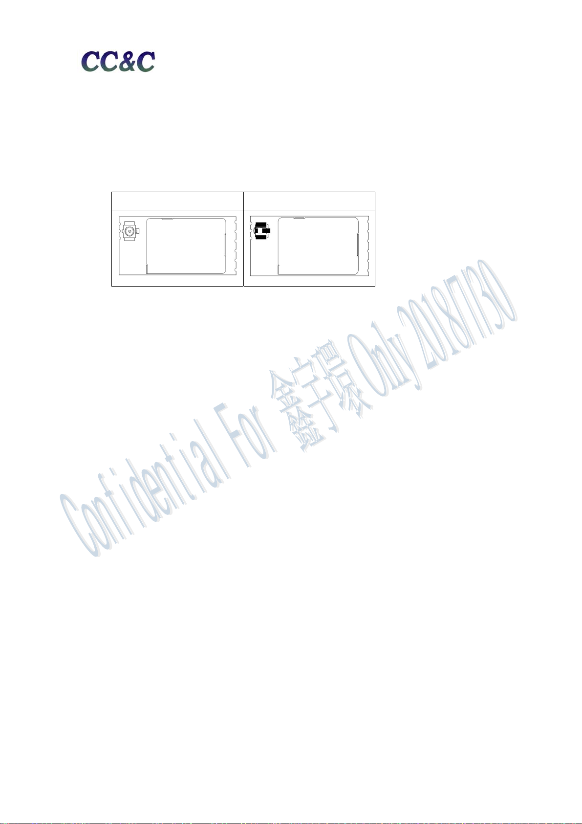
Factory options
DC power input 3.3V or 5V
RF output by RF connector(type-1),
RF output on half-hole(type-2)
RF type-1 RF type-2
`
4
晶訊科技股份有限公司 8F, No. 150, Jian Yi Road, Zhonghe District,
CC&C Technologies, Inc. New Taipei City, Taiwan 235, R.O.C.
Tel: 886-2-8226-5088 Fax: 886-2-8226-5077
General Specification
Model Name CM-8821CU
Product Name ac1x1+BT Module
Standard IEEE 802.11b/g/n/a/ac/ e/ h/ i/
Bluetooth v2.1+EDR/ v3.0/ v3.0+HS/ v4.2/
WLAN:
802.11b: 11, 5.5, 2, 1 Mbps
802.11g: 54, 48, 36, 24, 18, 12, 9, 6 Mbps
802.11n: MCS0 to 7 for HT20MHz, MCS0 to 7 for HT40MHz
Data Transfer Rate
802.11ac: MCS0 to 8 for HT20MHz, MCS0 to 9 for HT40MHz, NSS1
MCS0 to 9 for VHT80MH
Bluetooth:
Basic rate: 1Mbps
Enhanced data rate: 2, 3 Mbps
High Speed: 6, 9, 12, 18, 24, 36, 48, 54 Mbps
Modulation Method
Frequency Band 2.4GHz and 5GHz ISM Band
Spread Spectrum
Receiver Sensitivity
Antenna
Security
WLAN: CCK, DQPSK, DBPSK, BPSK, QPSK,16QAM, 64QAM, 256QAM
Bluetooth: 8DPSK, π/4 DQPSK, GFSKFSK
IEEE 802.11b: CCK (Complementary Code Keying)
IEEE 802.11g/n/a/ac:OFDM (Orthogonal Frequency Division Multiplexing)
Bluetooth: FHSS (Frequency Hopping Spread Spectrum)
WLAN:
-80dBm – 802.11b@11Mbps
-71dBm – 802.11g@54MBps
-67dBm – 802.11n@MCS7_BW20
-64dBm – 802.11n@MCS7_BW40
-57dBm – 802.11ac@NSS1_MCS9_BW20
-54dBm – 802.11ac@NSS1_MCS9_BW40
-51dBm – 802.11ac@NSS1_MCS9_BW80
Bluetooth:
-89dBm@1Mbps
-90dBm@2Mbps
-83dBm@3Mbps
IPEX Antenna x 1
WPA, WPA2
Operating Temperature
Storage Temperature -10 ~ 70°C ambient temperature
Humidity
Size 25 x 12 mm (L x W)
0 – 50° C ambient temperature
5 to 90 % maximum (non-condensing)
5

晶訊科技股份有限公司 8F, No. 150, Jian Yi Road, Zhonghe District,
CC&C Technologies, Inc. New Taipei City, Taiwan 235, R.O.C.
Tel: 886-2-8226-5088 Fax: 886-2-8226-5077
DC power input:(factory option)
Module Minimum Typical Maximum Unit
DC 5V module
DC 3.3V module
4.75 5 5.25 V
3.135 3.3 3.465 V
6

晶訊科技股份有限公司 8F, No. 150, Jian Yi Road, Zhonghe District,
CC&C Technologies, Inc. New Taipei City, Taiwan 235, R.O.C.
Tel: 886-2-8226-5088 Fax: 886-2-8226-5077
Pin outs define:
Pin Signal Input /Output Description
1 BT_LED Output BT LED Pin(Active Low)
2 VDD Power 3.3V or 5V by factory o pt ion
3 HSDM I/O High-Speed USB D- Signal
4 HSDP I/O High-Speed USB D+ Signal
5 GND - Ground
6 WL_LED I/O
7 GND - Ground
8 RFIO_OUT RF
9 GND - Ground
10 BT_WAKE_HOST Output
11 GPIO2 I/O General Purpose Input/ Output Pin
12 CHIP_EN Input
13 GPIO1 I/O General Purpose Input/ Output Pin
14 BT_DIS Input
15 GPIO8 I/O
16 HOST_WAKE_BT Input
17 WL_DIS Input Shared with GPIO9. This pin can externally shut down the
WLAN LED Pin(Active Low),
General Purpose Input/ Output Pin
WLAN(2.4G/5G)/BT RF port (if don’t using IPEX
connector)
Signal from module to wake up host,refer driver source
code for details.
This Pin Can externally shut down the RTL8821CU-CG(No
Extra Power Switch Required).
Shared with GPIO11. This pin can externally shut down the
RTL8821CU-CG BT function when BT_DIS is pulled Low.
When this pin is pulled low. USB interface will be also
disabled. This pin can be also defined as the BT Radio-off
function with host interface remaining connected
WLAN LED Pin(Active Low), shared with GPIO8
General Purpose Input/ Output Pin
Signal from host to wake up module,refer driver sou rce
code for details.
7

晶訊科技股份有限公司 8F, No. 150, Jian Yi Road, Zhonghe District,
CC&C Technologies, Inc. New Taipei City, Taiwan 235, R.O.C.
Tel: 886-2-8226-5088 Fax: 886-2-8226-5077
RTL8 821CU- CG WLAN function when WL_DIS is pulled
Low. When this pin is pulled low. USB interface will be also
disabled. This pin can also be configured as the WLAN
Radio-off function wit h ho st inte rface remaining connected
18 HOST_WAKE_WL Input
19 WL_WAKE_HOST Output
Signal from host to wake up module,refer driver sou rce
code for details.
Signal from module to wake up host,refer driver source
code for details.
The external circuits for WiFi and BT activity LED display
8

晶訊科技股份有限公司 8F, No. 150, Jian Yi Road, Zhonghe District,
CC&C Technologies, Inc. New Taipei City, Taiwan 235, R.O.C.
Tel: 886-2-8226-5088 Fax: 886-2-8226-5077
Block Diagram
9

Dimension
晶訊科技股份有限公司 8F, No. 150, Jian Yi Road, Zhonghe District,
CC&C Technologies, Inc. New Taipei City, Taiwan 235, R.O.C.
Tel: 886-2-8226-5088 Fax: 886-2-8226-5077
Subject to change without notice
10

晶訊科技股份有限公司 8F, No. 150, Jian Yi Road, Zhonghe District,
CC&C Technologies, Inc. New Taipei City, Taiwan 235, R.O.C.
Tel: 886-2-8226-5088 Fax: 886-2-8226-5077
PCB Layout footprint
The recommended layout pads for CM-8821CU module are shown below. (Module top view)
All dimensions are in millimeters.
Tolerance: +- 0.05mm
11

晶訊科技股份有限公司 8F, No. 150, Jian Yi Road, Zhonghe District,
CC&C Technologies, Inc. New Taipei City, Taiwan 235, R.O.C.
Tel: 886-2-8226-5088 Fax: 886-2-8226-5077
Reference Temperature Reflow Chart
This module is surface mount device; please refer below conditions for drying before
solder reflow processes. (extracted from IPC/JEDEC J-STD-033B.1)
Bake @ 125
Exceeding
floor Life
By > 72h
9 hours
o
C Bake @ 90 oC Bake @ 40 oC
Exceeding
floor Life
By ≤ 72h
7 hours
Exceeding
floor Life
By > 72h
33 hours
Exceeding
floor Life
By ≤ 72h
23 hours
Exceeding
floor Life
By > 72h
13 days
Exceeding
floor Life
By ≤ 72h
9 days
12

(OEM) Integrator has to assure compliance of the entire end-product incl. the integrated RF Module.
For 15 B (§15.107 and if applicable §15.107) compliance, the host manufacturer is required to
show compliance with 15 while the module is installed and operating.
Furthermore the module should be transmitting and the evaluation should confirm that the module's
intentional emissions (15C) are compliant (fundamental / out-of-band). Finally the integrator has
to apply the appropriate equipment authorization (e.g. Verification) for the new host device per
definition in §15.101.
Integrator is reminded to assure that these installation instructions
will not be made available to the end-user of the final host device.
The final host device, into which this RF Module isintegrated" hasto be labelled
with an auxilliary lable stating the FCC IDofthe RF
Module, such as "Contains FCC ID: PANCM8821CU
"This device complies with part 15 of the FCC rules. Operation is subject to the following two
conditions:
(1)this devicemay not cause harmful interference, and
(2)this devicemust accept any interference received, including
interference thatmay cause undesired operation."
NOTE: This equipment has been tested and found to comply with the limits for a Class B digital
device, pursuant to part 15 of the FCC Rules. These limits are designed to provide reasonable
protection
against harmful interference in a residential installation. This equipment generates, uses and can
radiate radio frequency energy and, if not installed and used in accordance with the instructions,
may cause harmful interference to radio communications. However, there is no guarantee that
interference will not occur in a particular installation. If this equipment does cause harmful
interference to radio or television reception, which can be determined by turning the equipment
off and on, the user is encouraged to try to correct the interference by one or more of the
following measures:
--Reorient or relocate the receiving antenna.
--Increase the separation between the equipment and receiver.
--Connect the equipment into an outlet on a circuit different from that to which the receiver is
connected.
--Consult the dealer or an experienced radio/TV technician for help.
Changes or modifications to this unit not expressly approved by the party responsible for
compliance could void the user's authority to operate the equipment.

Module statement
The single-modular transmitter is a self-contained, physically delineated, component
for which compliance can be demonstrated independent of the host operating
conditions, and which complies with all eight requirements of § 15.212(a)(1) as
summarized below.
1) The radio elements have the radio frequency circuitry shielded.
2) The module has buffered modulation/data inputs to ensure that the device will
comply with Part 15 requirements with any type of input signal.
3) The module contains power supply regulation on the module.
4) The module contains a permanently attached antenna.
5) The module demonstrates compliance in a stand-alone configuration.
6) The module is labeled with its permanently affixed FCC ID label
7) The module complies with all specific rules applicable to the transmitter, including
all the conditions provided in the integration instructions by the grantee.
8) The module complies with RF exposure requirements.
This transmitter/module must not be collocated or operating in conjunction with
any other antenna or transmitter.
This device is acting as slave and operating in the 2.4 GHz (2412 ~2462 MHz) band.
Ad Hoc function is supported but not able to operate on non-US frequencies.
FCC Radio Frequency Exposure Statement
The device has been evaluated to meet general RF exposure requirements. The device can be used in fixed/
mobile exposure conditions. The min separation distance is 20cm.
 Loading...