

Page 1

晶訊科技股份有限公司
CC&C Technologies, Inc.
User's Manual
BT5.0 Module
BM-52840
Manufacturer : Kunshan CC&C Technologies, Co., LTD.
Page 2

晶訊科技股份有限公司
CC&C Technologies, Inc.
Bluetooth 5 Module
Data Sheet
BM-52840
Description
BM-52840 is a Bluetooth 5 Low Energy
class 1 module that provides a complete
solution from various interfaces to different
sensors to BLE protocol stack and applica-
tions. It includes 32MHz crystal and a sys-
tem-on-chip Nordic nRF52840. The mini-
mal parts count and small footprint of the
BM-52840 is ideally suited for the re-
quirement of high integration Bluetooth
Low Energy technology in portable devices
and consumer electronics.
The system-on-chip architecture design of
the module makes a much smaller space
and minimal cost and simplifies the whole
system design.
1Mbs, 500 kbs, 125 kbs
Bluetooth 5 support for long range and
high throughput
AES 128-bit ECB/CCM/AAR hardware
accelerator
-96 dBm Sensitivity for Bluetooth low
energy
12 bit /200K SPS ADC
Application
Advanced wearables
• Connected watches
• Advanced personal fitness devices
• Wearables with wireless payment
• Connected health
• Virtual/Augmented Reality applica-
Features
Small footprint: 11.3×20×1.8mm
26-pin perforated hole.
Bluetooth 5 ready multiprotocol radio
Bluetooth 5 data rate support: 2 Mbs,
tions
Internet of Things (IoT)
• Smart home sensors and controllers
• Industrial IoT sensors and controllers
Interactive entertainment devices
• Advanced Remote controls
• Gaming controllers
8F, No. 150, Jian Yi Road, Zhonghe District, New Taipei City, Taiwan 235, R.O.C.
Tel: 886-2-8226-5088 Fax: 886-2-8226-5077
Page 3
晶訊科技股份有限公司
CC&C Technologies, Inc.
Revision History
Version Date Change Description
1.0 11/3, 2017 Initial release
Data Sheet
BM-52840
Note: All electrical and mechanical specifications may be changed by CC&C Technologies, Inc.
without notice.
No. 150, Jian Yi Road, Zhonghe District, New Taipei City, Taiwan 235, R.O.C.
8F,
Tel: 886-2-8226-5088 Fax: 886-2-8226-5077
Page 4
Data Sheet
3/10
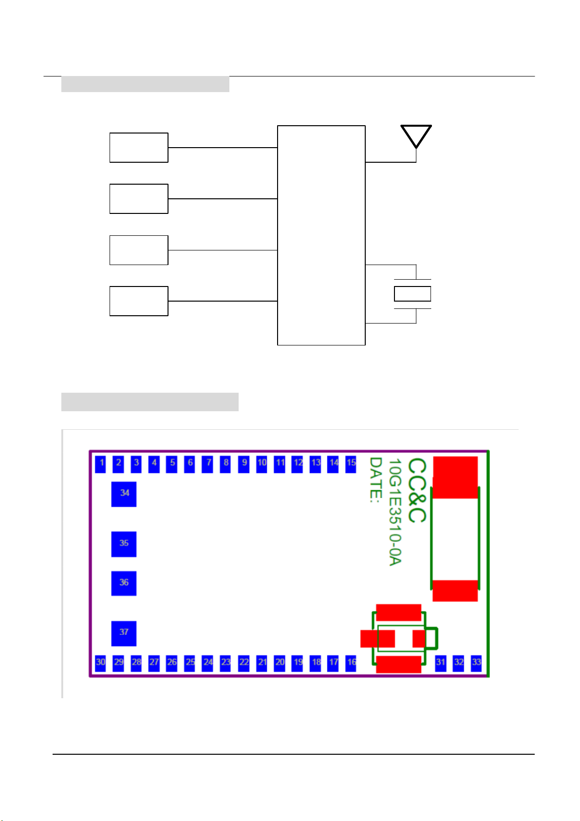
Functional Block Diagram
USB
SPI
UART
PWM
BM-52840
2402-2480MHz
Antenna
N52840
XTAL
32MHz
Pin Assignment (Top view)
BM-52840
Block Diagram
晶訊科技股份有限公司
CC&C Technologies, Inc.
Page 5

Data Sheet
4/10
Pin Definition
Pin Signal Function Description
1 GND Ground Ground
2 P0.17 I/O Programmable I/O
3 P0.12 I/O Programmable I/O
4 VBUS Power Operating supply voltage 4.35~5.5V
5 P0.29 GPIO. Programmable I/O , Analog input
6 GND Ground Ground
7 VDD Power Operating supply voltage 1.7~3.6V
8 P0.26 I/O Programmable I/O
9 P0.04 I/O Programmable I/O, Analog input
10 P0.01 I/O Programmable I/O
11 P0.02 I/O Programmable I/O, Analog input
12 P0.00 I/O Programmable I/O
13 P1.15 I/O Programmable I/O
BM-52840
14 DCC I/O DC/DC converter output
15 DEC4 I/O 1.3 V regulator supply decoupling
16 SWDIO Debug Debug serial data
17 SWDCLK Debug
18 P1.00 I/O Programmable I/O
19 P0.24 I/O Programmable I/O
20 P0.03 I/O Programmable I/O, Analog input
21 P1.14 I/O Programmable I/O
22 P1.13 I/O Programmable I/O
23 P1.11 I/O Programmable I/O
24 P0.10 I/O Programmable I/O
25 P0.09 I/O Programmable I/O
26 P1.06 I/O Programmable I/O
27 P0.18/RESET I/O Programmable I/O ,Configurable as system RESET
28 P1.02 I/O Programmable I/O
29 P1.04 I/O Programmable I/O
30 P0.20 I/O Programmable I/O
31 P1.10 I/O Programmable I/O
32
RFIO_OUT RF
Serial wire debug clock input for debug and programming
BT RF port
33 GND Ground Ground
34 VBUS Power Operating supply voltage 4.35~5.5V
35 USB_DP I/O USB D+
36 USB_DN I/O USB D-
37 GND Ground Ground
晶訊科技股份有限公司
CC&C Technologies, Inc.
Page 6

Data Sheet
5/10
SPECIFICATION
BM-52840
Product Name
Bluetooth 5.0 Module
Model Number BM-52840
Operating Frequency
Tx power(max)
2402-2480GHz
6dBm
Receiver sensitivity -96dBm
Power Voltage Range
Symbol Description Min. Typ. Max. Units
VBUS System power voltage 4.3 5 5.5 V
VCC_IO I/O power voltage -0.3 3.9 V
Tx mode 0dBm 11.6 mA
Current
Tx mode 6dBm
27.6 mA
Consumption
Rx mode 12.9 mA
Storage Temperature -40 25 125
o
C
晶訊科技股份有限公司
CC&C Technologies, Inc.
Page 7

Data Sheet
6/10
BM-52840
APPLICATION CIRCUIT
The application circuit of BM-52840 is shown below. It uses a UART-to-USB converter
IC PL-2303 so developing firmware on PC becomes more convenient.
USB_5V
P020
P104
P102
P106
P010
P009
RESET_N
P111
P002
VCC3.3V
USB_5V
GND
P017
P012
P029
GND
P026
P004
U2
1
GND
2
I2C_SCL
3
I2C_SDA
4
NC
5
DIO_14
6
GND
7
VDD
8
JTAG_TMSC
9
JTAG_TCKC
29
30
GND28GND
P113
26
23
NC24NC25NC
reset
GND27GND
N52840
USB_DP
USB_DN
20NC22
21
37
NC34NC36NC35NC
DIO_0
DIO_1
P017
P029
P004
P000_RT P002_TX
P115_CT
J10
2
1
4
3
6
5
8
7
10
9
CONN SOCKET 5x2
P012
P026
P001_RX
P100
P002
P113
P010
P106
J2
2
1
4
3
6
5
8
7
10
9
CONN SOCKET 5x2
P024
P114
P111
P009
P102
CON1
VBUS
DD+
ID
GND0
GND1
GND2
MINI USB Connector
P002_TX
P001_RX
P115_CT
P000_RT
CON2
5
VBUS
4
D-
3
D+
2
ID
1
GND0
6
GND1
7
GND2
MINI U SB Connector
5
4
3
2
1
6
7
VO_33
USB_5V
R16 0
D5
SK34A
R13 33
R14 33
BEAD/0402
R20
0
0.1uF
R23 0
R40 0
R41 0
R46 0
D6
SK34A
L4
BEAD/0402
L2
VO_33
C11
VO_33
R17 1.5K
R18 27
R19 27
GND
USB_UART_5V
C6
47PC747P
UART_RX
UART_CTS
UART_TX
UART_RTS
UART_TX
UART_RX
UART_CTS
UART_RTS
USB_UART_5V
VO_33
USB1_DM
USB1_DP
DIO_1310DIO_1211DIO_1112DIO_1013DIO_614DIO_515DIO_916DIO_417DIO_318DIO_2
DCC
P002_TX
P115_CT
P000_RT
P001_RX
USB_5V
USB_DN
USB_DP
30
31
32
U4
33
1
2
3
4
5
6
7
8
TXD
Bot _PAD
RTS-T
DTR_N
VDD_325
RXD
RI_N
PL-2303HXD- QFN32
GND
VDD_3.3
DSR_N
DCD_N
CTS_N
SHTD_N9GP310GP211NC12NC13DP14DM15NC
USB -> UART
DEC4
SWDIO
C8
2.2u
19
P024
P100 P114
SWDCLK
C3
0.1u
27NC28NC29
RESERVED
NC32NC33NC
31
1
J11
CONN PLU G 1x1
R47
1K
25
26
GND
TEST
NC
GP1
GP0
NC
VDD_5
RESET_N
GND
VO_3.3
16
USB1_DM
USB1_DP
P009
CC2640_Module
2
TP1
NC/I PEX connector
GND
1
IN
GND
3
BT Antenna
R15 NC/0
U3 iD9302
5
VOUT
1
VIN
2
VSS
CE3NC
24
23
22
21
20
19
18
17
C12
0.1uF/0402
C13
0.1uF
4
VO_33
C4
0.1u
C15
10uF/0603
Slide switch
VCC3.3V
R36
10K
SW13
P010
R31
10K
C5
2.2u
NC/Bat tery Jack (CR 2032)
USB_UART_5V
SW14
VCC3.3V
SWDIO
SWDCLK
J5
12
CONN PLUG 1x1
J7
CONN PLU G 1x1
VBATT
J8
1
1
2
Left: +
2
Right: -
VO_33
R21
10K
C14
0.1uF
LED IND
VCC3.3V
R38
10K
R37
P111 P113
10K
J6
1
2
3
4
P104P020
1 2
J9
CONN PLU G 1x1
Monitoring battery
VCC3.3V
12
Button
P020
R27
1K
VCC3.3V
VCC3.3V
R29
10K
S1
Q1
1R1001
P106
D1
BLE_LED
R24
470R
VCC3.3V
P104
R34
NC
R35
NC
VCC3.3V
AIO
S2
P102
R30
10K
VCC3.3V
R28
1K
RESET_N
VCC3.3V
D2
BLE_LED
R25
470R
Q2
1R1001
L6
NC/15nH
L5
NC/10uH
DCC DEC4
VCC3.3V
R39
NC
R42
NC
R32
10K
R33
10K
USB_5V
D4
RED_LED
R26
470R
晶訊科技股份有限公司
CC&C Technologies, Inc.
Page 8

Data Sheet
7/10
Package Diagram
The thickness of BM-52840 is 1.8mm.
BM-52840
晶訊科技股份有限公司
CC&C Technologies, Inc.
Page 9

Data Sheet
8/10
Pad Dimensions (bottom view)
BM-52840
晶訊科技股份有限公司
CC&C Technologies, Inc.
Page 10

Data Sheet
9/10
BM-52840
Placement Guideline
It is recommended that BM-52840 be placed on the corner of the main board or
near the edge as shown below.
On the corner
Near the edge
However, placing BM-52840 inside the main board affects the RF performance and
may reduce the RF range significantly.
晶訊科技股份有限公司
CC&C Technologies, Inc.
Page 11

FCC Warning
This device complies with Part 15 of the FCC Rules. Operation is subject to the following two conditions:
(1) this device may not cause harmful interference, and
(2) this device must accept any interference received, including interference that may cause undesired operation.
NOTE: Any changes or modifications to this unit not expressly approved by the party responsible for compliance
could void the user's authority to operate the equipment.
FCC Radiation Exposure Statement:
This equipment complies with FCC radiation exposure limits set forth for an uncontrolled environment. End
users must follow the specific operating instructions for satisfying RF exposure compliance.This transmitter must
not be co-located or operating in conjunction with any other antenna or transmitter.
Note 1: Compliance of this device in all final host configurations is the responsibility of the Grantee.
OEM integrators are responsible to satisfy RF exposure requirements. SAR evaluation is valid for portable,
mobile and fixed applications.
Note 2: Any modifications made to the module will void the Grant of Certification, this module is limited to OEM
installation only and must not be sold to end-users, end-user has no manual instructions to remove or install the
device, only software or operating procedure shall be placed in the end-user operating manual of final products.
Note 3: The device must not transmit simultaneously with any other antenna or transmitter.
Note 4: To ensure compliance with all non-transmitter functions the host manufacturer is responsible for ensuring
compliance with the module(s) installed and fully operational. For example, if a host was previously authorized as
an unintentional radiator under the Declaration of Conformity procedure without a transmitter certified module
and a module is added, the host manufacturer is responsible for ensuring that the after the module is installed and
operational the host continues to be compliant with the Part 15B unintentional radiator requirements. Since this
may depend on the details of how the module is integrated with the host, CC&C Technologies, Inc. shall provide
guidance to the host manufacturer for compliance with the Part 15B requirements.
Note 5: FCC ID label on the final system must be labeled with “Contains FCC ID: PANBM52840”
The transmitter module must be installed and used in strict accordance with the manufacturer's instructions as
described in the user documentation that comes with the host product. CC&C Technologies, Inc. is responsible for
the compliance of the module in all final hosts.
 Loading...