

Page 1
(without price)
ZD-3
MD CD SYSTEM
SEP. 2000
INDEX
Page 2

Specifications................................................................................................................................... 1
Disassembly Instruction ................................................................................................................... 2
Reassembly of Tuning Pointer ......................................................................................................... 5
Block Diagrams................................................................................................................................ 6
Tuner.......................................................................................................................................... 6
AMP ........................................................................................................................................... 7
MD ............................................................................................................................................. 8
CD.............................................................................................................................................. 9
VR, Display , PS........................................................................................................................ 10
CD Pickup Replacement ................................................................................................................ 11
Tuner Adjustments......................................................................................................................... 12
Troubleshootings............................................................................................................................ 16
CD............................................................................................................................................ 16
MD ........................................................................................................................................... 25
PCB Views ..................................................................................................................................... 30
Tuner/SW PCB Top View ......................................................................................................... 30
AMP/Jack PCB Top View ......................................................................................................... 31
VR PCB Top View .................................................................................................................... 32
PS/SW A/SW B PCB Top View................................................................................................ 33
CD/Door PCB Top/Bottom Views ............................................................................................. 34
Display PCB Top/Bottom Views ............................................................................................... 36
BD PCB Top/Bottom Views ...................................................................................................... 37
Wiring Diagram .............................................................................................................................. 39
IC Lead Identification and Internal Diagrams ................................................................................. 40
Schematic Diagrams ...................................................................................................................... 57
Tuner........................................................................................................................................ 57
AMP ......................................................................................................................................... 58
CD............................................................................................................................................ 59
MD ........................................................................................................................................... 61
VR, LCD................................................................................................................................... 63
Exploded Views.............................................................................................................................. 64
Unit Assembly .......................................................................................................................... 64
Case Unit ................................................................................................................................. 67
Top Case Unit .......................................................................................................................... 68
MD Mechanism Unit................................................................................................................. 69
CD Mechanism ........................................................................................................................ 70
Parts List ........................................................................................................................................ 71
CONTENTS
Page 3

1
SPECIFICATIONS
MD SECTION
System: MiniDisc digital audio system
Laser: Semiconductor laser
Error correction: Advanced Cross Interleave read Solomon code (ACIRC)
Channel: 2 channels
Frequency response: 20 to 20,000 Hz ! 3dB
Wow and flutter: Less than measurement limit
Recording system: Magnetic field modulation overwrite method
Coding: Adaptive Transform Acoustic Coding (ATRAC)
CD SECTION
System: Compact disc digital audio system
Laser: Semiconductor laser
Channel: 2 channels
Fequency response: 20 to 20,000 Hz ! 3dB
Wow and flutter: Less than measurement limit
TUNER SECTION
Tuning range: FM: 88 to 108 MHz
AM: 530 to 1,600 kHz
Antenna: FM: Telescopic antenna
AM: Loop antenna (supplied)
GENERAL SECTION
Dimensions: 354 (W) x 155 (H) x 253 (D)
Weight: 3.7 kg (without batteries)
Power source: AC 230V, 50 Hz
DC 12V, 8 x “D” size (LR20)
Power consumption: 22W
Output power: 2.0 (W) + 2.0 (W)
Accessories: AC power cord
AM loop antenna
Instruction manual
Design and specifications are subject to change without prior notice.
IMPORTANT: This product is capable of substantial uses
that do not constitute infringement under the copyright
laws. It is sold for such uses, and it should not be used to
infringe the copyrights of others.
Page 4
DISASSEMBLY INSTRUCTIONS
1. Remove the battery cover.
2. Remove eight screws A holding the case B unit.
3. Open the CD door and remove three screws B holding the case ass’y.
2
Case B ass’y
CD door
Top case ass’y
Case ass’y
A
A
A
B
B
Page 5
D
D
C
E
F
F
3
4. Remove four screws C holding the MD holder A
and MD mechanism ass’y.
5. Remove five screws D holding the display unit.
6. Remove the three PCB supports holding AMP
PCB. (reffer figure)
Display unit
MD Holder A
MD Mechanism ass’y
AMP PCB ass’y
PCB
support
Case ass’y
Pinch the under PCB supports.
7. Remove four screws E holding the front panel ass’y.
8. Remove eight screws F holding the SP panel ass’y.
Case ass’y
SP panel ass’y
Front panel ass’y
Page 6
G
M
M
L
L
K
H
J
J
9. Pull out the two volume key ass’y , function key and band key.
10. Remove screw G holding the door SW PCB.
11. Remove six screws H holding the CD unit ass’y.
12. Remove four screws J holding the ESD spacer and tuner unit ass’y.
13. Remove five screws K holding the VR unit ass’y .
14. Remove two screws L holding the CD mechanism stopper.
15. Remove for screws M holding the CD mechanism ass’y.
4
Volume key ass’y
Function key
Band key
Volume key ass’y
Door SW PCB
VR unit ass’y
Tuner unit ass’y
CD
mechanism
ass’y
CD mechanism
stopper
CD
mechanism
stopper
ESD spacer
CD unit ass’y
Top case ass’y
Page 7

1
2
3
4
5
REASSEMBLY OF TUNING POINTER
1. Turn the varicon unclockwise stop position.
2. Set the tuner gear figuer position and fixed the screw.
3. Fixed the tuner chassis on the tuner PCB. (three screws)
4. Set the pointer to the tuner chassis mark position.
5. Fixed the tuner shaft screw A.
Tuner shft
Tuner gear
Mark
Pointer
Tuner chassis
Tuner PCB
Screw A
5
Varicon
Page 8
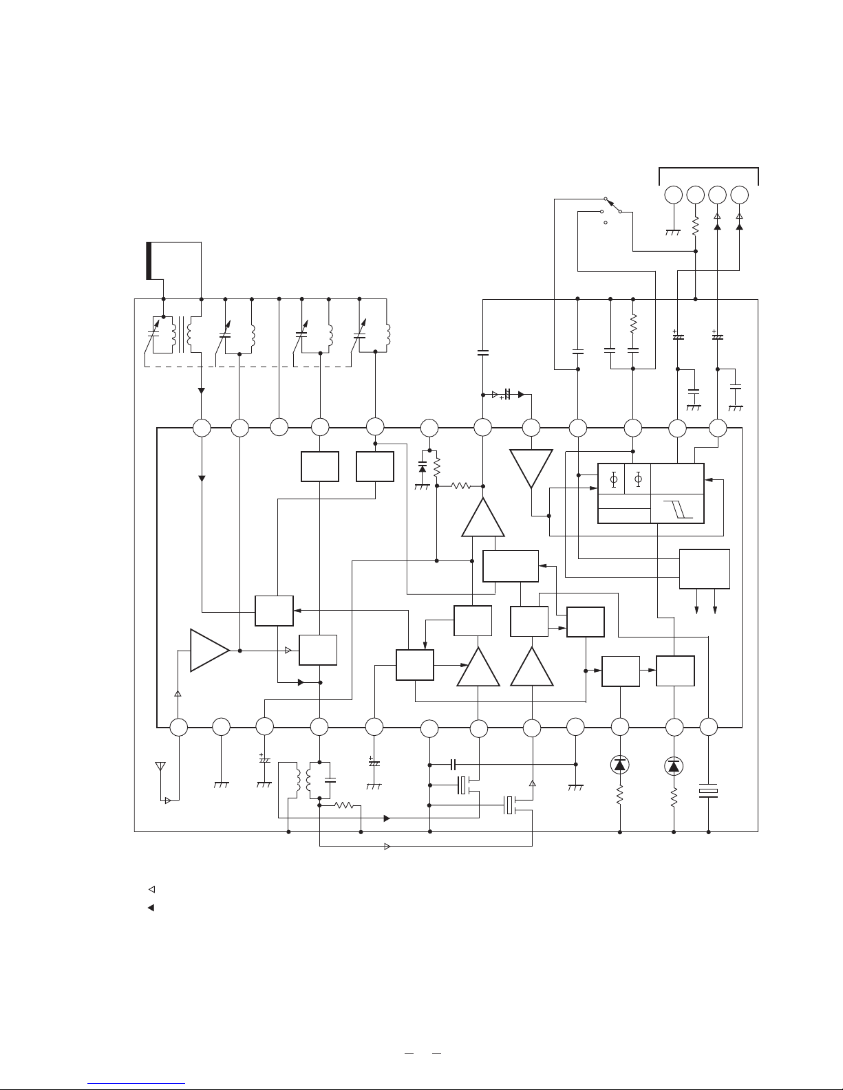
BLOCK DIAGRAMS
TUNER
6
Decode
TUN
LED
ST
LED
Level
DET
AM RFInFM RF
Out
RF VCCFM
OSC
AM
OSC
DET
Out
MPX
In
LPF1
LPF2
GND VCC R ch L ch
FM
RF In
RF
GND
AM Low
Cut
MIX Out
AGC
V
CC
AM IF
In
FM IF
In
GND
QUAD
To Amplifier Block
19 18
17
16 15
14
1324
Bar
Antenna
L1
L4
L3
SW1
BAND SWAM
FMStereo
FM-MONO
FM
Antenna
CF1
CF2
FM Signal
AM Signal
L6
1
3
4 5
76
8
9 10
11
12
AM
MIX
FM
RF
23
2122
FM
OSC
20
AM
OSC
FM
MIX
2
AGC
AM
DET
FM
Mute
AF
BUFF
AM
IF
FM
IF
FM
DET
AF
VCO
Divice
ST/MO
FM/AM
CF3
TUN
LED
ST
LED
31 2 4
CN3
AM Loop Antenna
Page 9
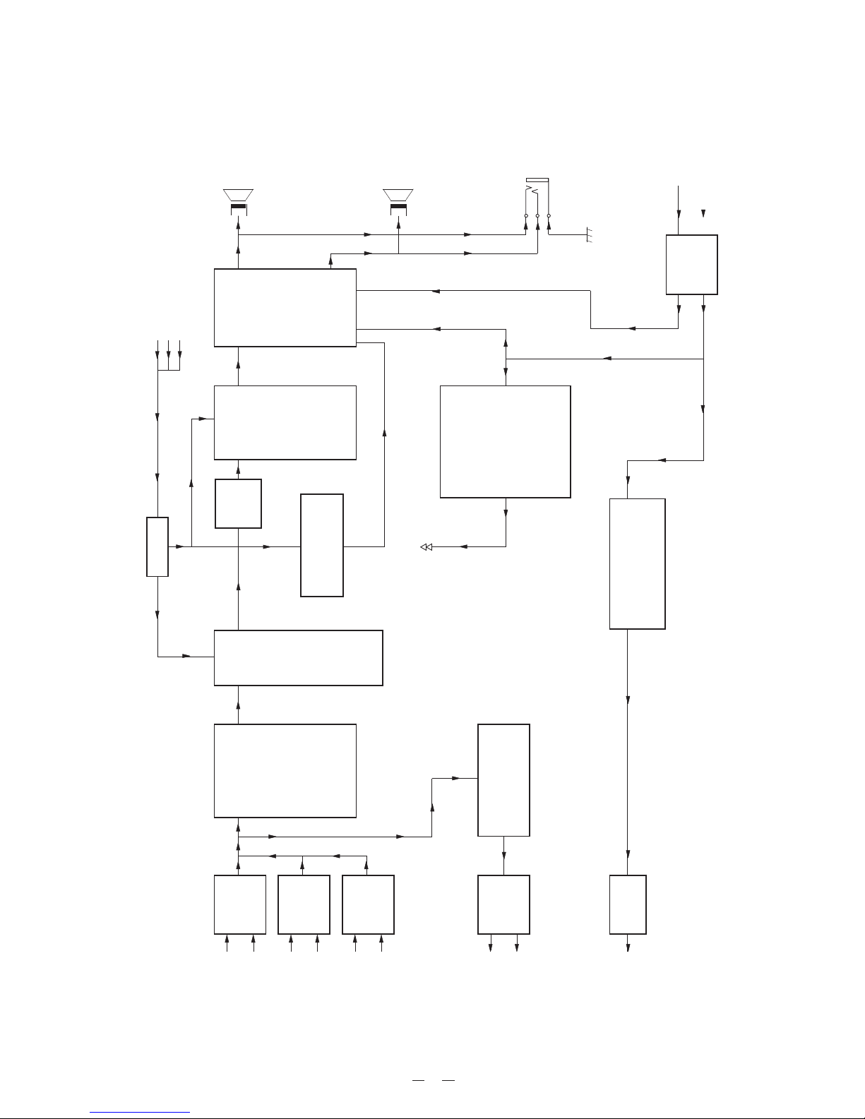
SURROUND
BBS
AFMUTE
CN303
CN301
CN302
Equalizing
Circuit
Q101, Q201
Speaker
L ch
Speaker
R ch
J301
Lipple Filter Circuit
Q303, Q304
MD Power Supply
Circuit
IC303
CN307
Power
Amplifier
Circuit
IC302
Mute
Circuit
Q104,
Q204
BBS
Circuit
IC301
CN303
Record Amplifier
IC300
(DC 7V)
CN301
CN303
MD Play L ch
MD Play R ch
CD Play L ch
CD Play R ch
Tuner In L ch
Tuner In R ch
MD Record L ch
MD Record R ch
MD 5V (DC)
Rotary
Volume
CN304
Surround
Circuit
Q301, Q302
AMP
7
Page 10
CN301
RX1
From CD DOUT
BD UNIT
MDOUT L
ADIN L
AGND
ADIN R
MDOUT R
DGND
HGND
MGND
D+5V
H+5V
M+5V
CN601
MD MUTE
RXD
TXD
RTS
RST
P DOWN
CTS
TEMP DET
CN402
H+5V
M+5V
D+5V
D+3V
A+3V
Power
Supply
IC601
DRAM
IC302
AD/DA
IC501
LPF
IC502
DSP
IC301
System
Control
IC401
RF-AMP
IC101
EEPROM
IC402
OPT
PU
M+5V
Motor
Driver
IC202
M
Loading
FO
TR
CN401 CN201
M
M
Spindle
Sled
CN401
PROTECT
REFRECT
CHACK IN
REC P
PB P
LIMIT IN
M+5V
H+5V
Head Coil
Driver
IC102, Q105,
Q106
Motor
Driver
IC402
CN102
MD MECHA UNIT
OW Head
MD
8
Page 11

4754-032-0
Q702,
Q703
to MD
CN705
to Front
to MD Control
to AMP
Q706, Q707
PS DET Circuit
to VOL
+3.3V
+8.0V
+3.3V
TR-
TR+
FO-
FO+
PD
LD
FEDBC
A
CN701
to Pick Up
to Mecha
KSM-213CJM
PSET
SPSPSL
SL
CN702
1
654
3
212210
9
28277
6
151416
13
12
10
Q701
Laser
Power
Control
PD
LD
F
E
PD2
PD1
83467
5
35
34
393837
36
OUT3+
OUT3-
OUT2+
OUT2-
OUT4+
OUT4-
OUT1-
OUT1+
IC703
BA6898S
Pick Up Mother Driver
VIN-3
VIN-2
VIN4
VIN-4
VIN-1
IC710
BA4510F
Tracking Assist
Circuit
19
11
29
30
4
IC701
CXA2542AQ
System Servo Processor
FEO
TA-O
SL-O
SL-P
TEO
RFO
CLK
XLT
DATA
C-OUT
SENS1
FOK
XRST
SENS2
5
12
15
41
311819202223252124
13
GFS
RF
IC702
CXD3009Q
Digital Signal Processor
SPOA
MDP
DOUT
LOUT1
ROUT2
SCOR
SQCK
SQSO
DATA
XLAT
CLOK
SENS
XRST
FOK
15
21
CN704
1
53
49
35
67
74
CN703
4
2
6
1
7
5
SW701
Door SW
49
644745272625242829
23
SCOR
SQCK
SQSO
DATA
XLT
CLK
SENS1
XRST
FOK
SENS2
DOOR SW
AFMUTE
LMUTE
SURROUND
BBS
RST
PSDET1
PWR/KEY
KEY3
PS-CONT
F TUNER
FMD
FCD
TEMP
DET
PDOWN
RESET
CTS
RTS
TXD
RXD
MUTE
DB3
DB2
DB1
DB0
E
CLK
KEY0
KEY1
KEY2
IC704
CXP740056
Sistem Control
CN706
63
66
67
65
68
70
69
80
8
6
5
4
7
2
3
1
18
17
16
15
14
13
62
61
60
3
4
5
6
7
8
11
12
13
IC707
S-80727AL-AQ-T1
Reset
CN707
Q708, Q709, Q710
REG CD Driver
IC709
PQ15RW11
REG-CD System
IC708
PQ15RW11
REG-Sistem
1
2
97
96
40
79
84
59
9
91
92
93
86345911
12
57
45789
6
79
18
CD
9
Page 12
4754-015-0
To
VR Unit
(GND)
(VCC)
WC 400
(C406)
Rectification
Circuit
D402~D405
Fuse
F401
Power
TRANS.
T401
J401
AC Jack
AC Cable
LCD Module
LCD950
LCD Driver
IC950
WC950
(GND)
(3.3V)
(DB3)
(DB2)
(DB1)
(DB0)
(E)
(CLK)
Control
Switch Circiut
SW970~SW974
SW980~SW984
SW990~SW994
(GND)
(KEYIN)
(KEYIN)
(KEYIN)
(VCC9V)
Stand-by LED
LD950
From CD Unit
From
AMP
Unit
(VCC9V)
(DC9V)
(GND)
(TU9V)
(MD9V)
WC307
WC304
Rotary Volume
With
Loundness
VR350
Control Switch
Circuit
SW350~SW352
Lipple Filter
Circuit
Q350, Q351,
Q352
Function
Switch
S353
WC350
From CD Unit
(VCC9V)
(GND)
(Power Key)
(Key IN3)
(PS CONT)
(DC9V)
(GND)
(CD9V)
(F TU)
(3.3V)
(F MD)
(F CD)
CN400
From
PS
Unit
(VCC9V)
(GND)
VR
DISPLAY
PS
4754-009-0
4754-036-0
10
Page 13
CD PICKUP REPLACEMENT
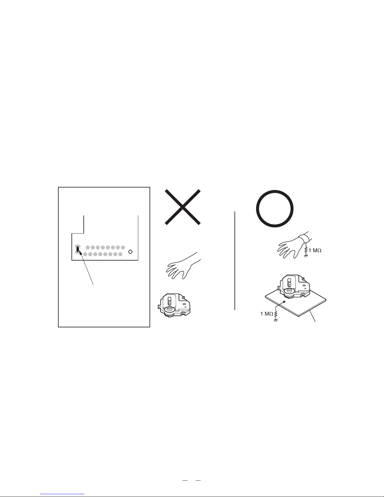
PRECAUTIONS
To prevent damage caused by static electricity, the following procedures for grounding is required when opening
or repairing the unit.
1. Grounding for the human body
Be sure to put on a wrist-strap for grounding (with impedance lower than 106 Ω) whose other end is grounded.
The strap works to drain away the static electricity build-up on the human body .
2. Grounding for the work table
Be sure to lay on the table a conductive sheet (with impedance lower than 106 Ω) such as a sheet of copper
which is grounded.
3. As static electricity build-up on clothes is not drainded away, be careful not to let your clothes touch the unit.
4. The short-pad on the pick-up PCB of a spare part is short-circuited for protection during shipment. To open the
short circuit, remove the soldering quickly with a soldering iron whose insulation resistance is larger than
10MΩ after connection to a suitable APC circuit.
11
Short-pad on pickup PCB
[Note] After the wire connector is
connected, desolder( short-pad).
1. Wrist-strap
for grounding
2. Conductive sheet
Pickup
Page 14

12
TUNER ADJUSTMENTS
Remarks:
* When aligning the range and adjusting tracking, proceed with alignment in a sequence of AM t FM.
* Use a screwdriver with a plastic grip for all alignments.
Equipment Required
* AM signal generator (AM SG)
* Loop antenna
* Output meter
* Oscilloscope
* FM signal generator (FM SG)
* Screw driver (Plastic type)
* Dummy load 32 Ω
Page 15
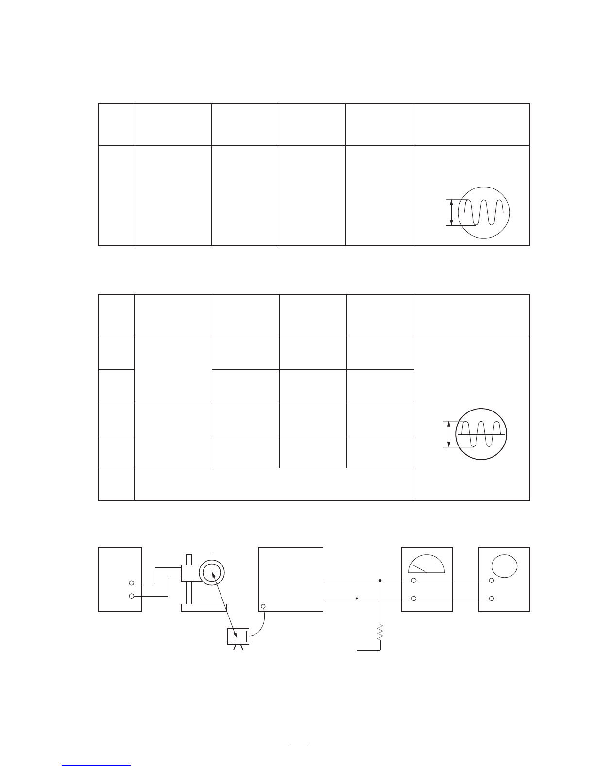
AM IF Alignment (Figures 1 and 3)
Step
Alignment
Frequency
of signal
generator
Tuning
dial
setting
Adjustment Remarks
IF calibratoion
1000 KHz 1000 end L6 Obtain sine-wave and
maximum amplitude.
AM Alignment (Figures 1 and 3)
Figure 1
Max.
13
Adjustment of
tracking
530 KHz
Low End
L2
Obtain sine-wave and
maximum amplitude.
1
1600 KHz
High End
AM-OSC2
3 Repeat the above adjustments.
Step Alignment
Frequency
of signal
generator
Tuning
dial
setting
Adjustment
Remarks
Tuning range
calibration
600 KHz 600 KHz L1
1
2 1400 KHz 1400 KHz AM-ANT
Max.
Output meterAM SG Loop antenna
Set
Osilloscope
Dummy load
32 Ω
60 cm
J301
Headphone jack
GND
Loop antenna
(Accessory)
CH1
Page 16
FM Alignment (Figures 2 and 3)
Output meterFM SG Set Oscilloscope
Dummy
load
32 Ω
GND
Figure 2
FM dummy load
R1=Output impedance
of FM SG
R2=75 Ω - R1/2 Ω
FM ANT
GND
R1
R2
Adjustment of
tracking
88 MHz
Low End
L3
Obtain sine-wave and
maximum amplitude.
1
108 MHz
High End
FM-OSC2
3 Repeat the above adjustments.
Step Alignment
Frequency
of FM signal
generator
Tuning
dial
setting
Adjustment
Remarks
Tuning range
calibration
90 MHz 90 MHz L4
1
2 106 MHz 106 MHz FM-RF
Max.
4754-022-0
14
J301
Headphone jack
Page 17
C28
C31
R3
CF3
IC1
C30
CF2
R4
Q1
C29
R16
L6
R15
R14
R21
C6
C5
C34
C19
C20
C6
C7
BF1
C21
R5
CF4
CF1
R12
C12
C27
D3
D4
CN1
CN2
D2
D1
C10
L5
C8
C11
L1
L4
R1
C4
C2
R8
L3
C14
R6
C3
D5
R2
C7
VC1
L2
R13
C18
C20
D8
C19
TUNER PCB
4754-520-2-91
CN3
R11
CN4
C16
C33
C32
R17
C24
R18
C13
R7
C25
C15
C17
C22
C26
R9
R10
C23
1
12
13
24
TUNER ADJUSTMENT POINTS (TUNER PCB)
15
Top View
Figure 3
FM RF
FM OSC
AM ANT
AM OSC
RF GND
FM ANT AM ANT
GND
Page 18

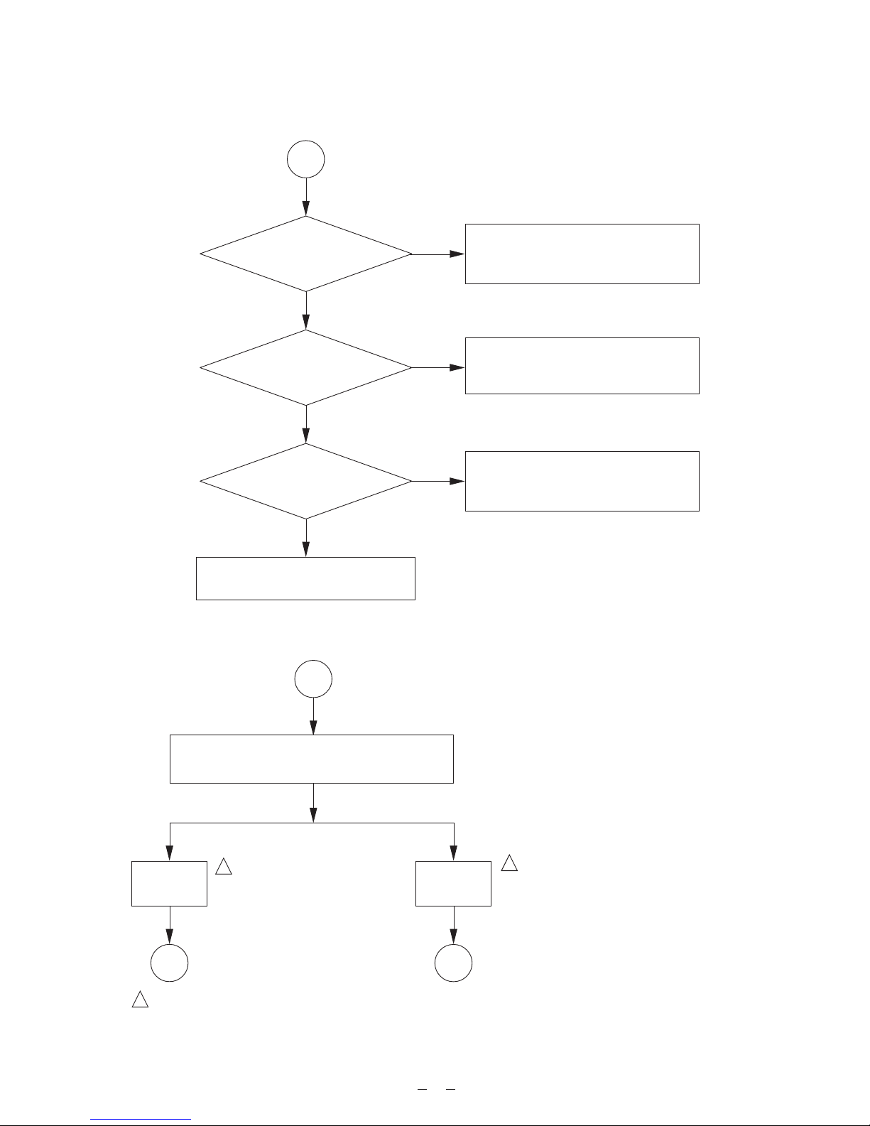
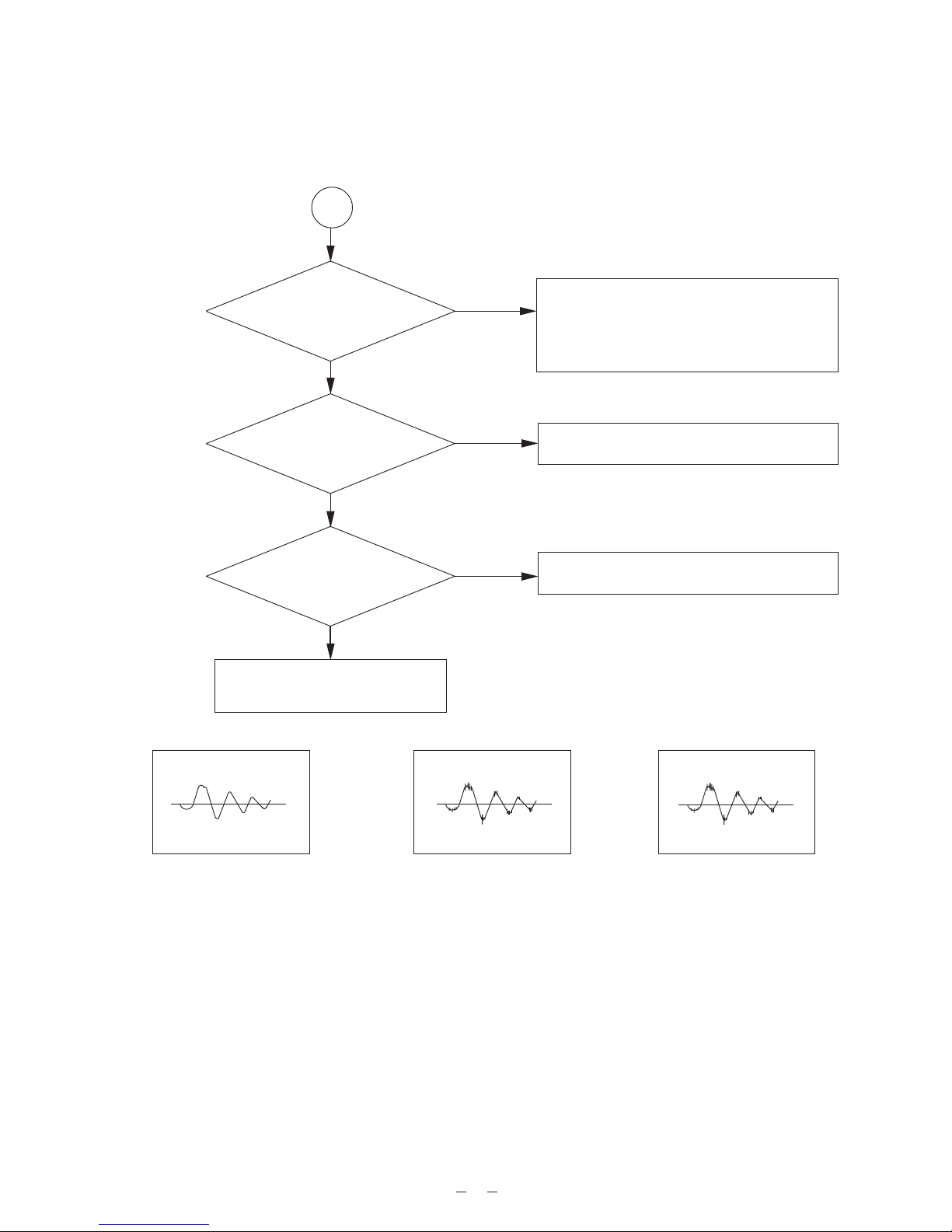
TROUBLESHOOTINGS
Is ” NO DISC”
displayed after “READ”
displayed ?
1
Is the audio signal
present at output
terminals ?
3
5
OK
No
Yes
No
No
Yes
Yes
2
Yes
NoAre total track
numbers and playing
time displayed ?
Can FR and FF be
operated normally ?
Can track number be searched
smoothly ?
4
No
Yes
Power switch on and set function
switch for CD position.
Press FR or FF button.
Turn jog knob to left or right.
Does the audio signal
(digital) present at output
terminals ?
Record on MD from CD.
Load a disc close CD door.
Press CD “ / “ button.
16
CD
Page 19
Is system +3.3 V lines
normal ?
No
Yes
* IC708 or IC709 is defective.
* Check circuit around IC708 and IC709.
Is pin 40 (RESET)
of IC704 high ?
No
Yes
* IC707 is defective.
* Check circuit around IC707.
Does 12 MHz
clock pulse appear at
pin 43 of IC704 ?
No
Yes
* X702 is defective.
* IC704 is defective.
* Check circuit around X702 and IC704.
* Check IC704.
* Check circuit around IC704.
Repair Item 1: ” NO DISC” is not displayed after “ READ” displayed.
A B
Less than
8 sec
More than
8 sec
2
Check how long it takes until “ NO DISC” is
displayed after CD door has closed.
Repair Item 2: Total track number and playing time are not displayed.
1
Note: That shows the time it takes until “ NO DISC” is displayed from when CD tray has been closed perfectly.
Check pickup whether there is it at home position.
!
!
!
17
Page 20
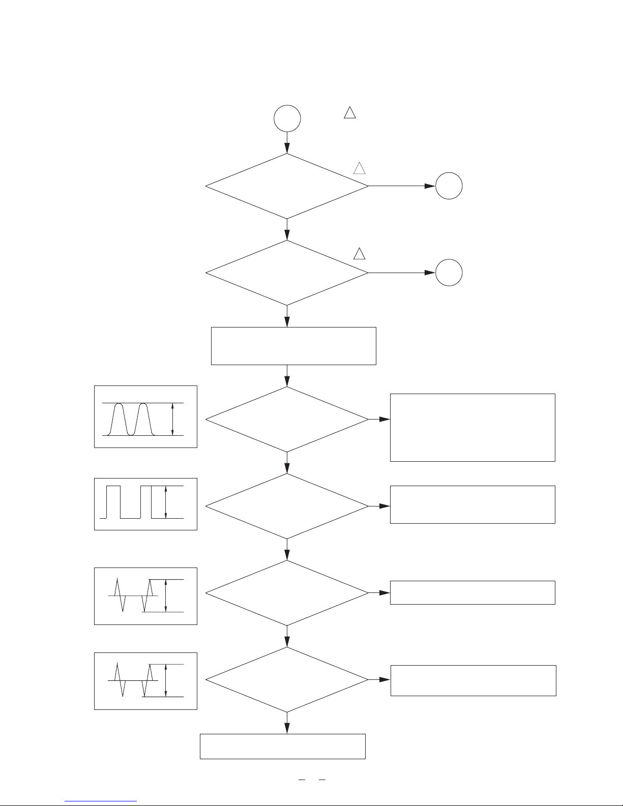
Repair Item 2-A
Note: Open the CD door and check the radiation
power with an optical power meter or by watching
the radiaation through the lens of the pickup unit at
a minimum distance of 30cm from the pickup.
Does the LASER emit ?
Dose the lens move
up and down ?
Load a disc and close CD door.
Then check the following.
Is the waveform
at pin 25 (FOK) of IC701 like
that shown in figure 5 ?
* IC701 is defective.
Is the waveform
at pin 31 (RFO) of IC701 like
that shown in figure 4 ?
* Check FFC connector (CN701) from
pickup.
* Check soldering IC701. IC702 and
IC703.
* IC701 is defective.
* Pickup is defective.
Is the waveform
at pin 48 (FEO) of IC701 like
that shown in figure 6 ?
* Check soldering pins 25, 26 and 27
of IC701.
* IC701 is defective.
* Check circuit around IC801.
No
No
No
No
No
Yes
Yes
Yes
Yes
Yes
Figure 4
Figure 5
E
3.3V
!
!
!
E=nearly 1V
Is the waveform
at pin 1 (FEI) of IC701 like
that shown in figure 7 ?
No
Yes
Figure 6
>2V
Figure 7
>1V
* Check circuit around pins 1 and 48 of
IC701.
A
A1
A2
18
Page 21
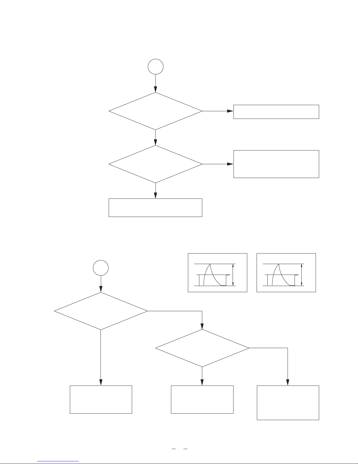
1.6VVC3.6VVC
Figure 20
Is pin 34 of IC701
more than 2.0V at
playing ?
* Check circuit around pin 34 of
IC701.
* Check digital signal pins 18, 19
and 20 of IC701.
* Check FFC connector (CN701).
* Pickup is defective.
No
Yes
Repair Item 2-A2: The lens does not move up and down.
Is waveform at
pins 13 and 16 of CN701 like that
shown in figuer 8 ?
* Check FFC connector
from pickup.
* Pickup is defective.
Is waveforn at
pin 5 (FEO) of IC701 like
that shown in figuer 9 ?
No
No
Yes
Yes
* Check circuit around
IC701.
* IC701 is defective.
* Check circuit around
and soldering pin 16 of
IC701.
* IC701 is defective.
* IC702 is defective.
Figure 21
Is emitta of Q701
3.3V ?
* Check soldering Q701.
No
Yes
Repair Item 2-A1: The laser does not emit.
A1
A2
19
Page 22
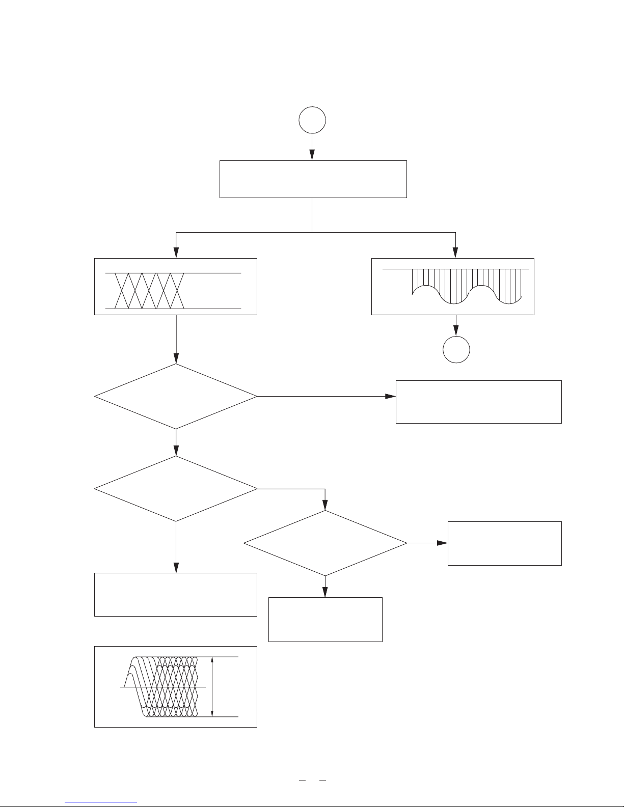
Repair Item 2-B
Watch the waveforn at pin 31 (RFO) of
IC801 an oscilloscope.
Is waveform at
pin 35 (RF) of IC702 like that
shown in figure 10 ?
Is pin 49(GFS) of of IC702
high ?
* Check circuit around C and pin 35 of
IC702 (RF).
* IC702 is defective.
* Check pins 29, 30 and 31 of IC702.
* Check pins 17 and 49 of IC702.
* IC702 is defective.
No
No
Yes
Yes
Figure 10
Waveform
Does 16.93 MHz appear
at pin 70 (XTAL) of IC702 ?
Yes
* Check crystal and circuit
around it.
* IC702 is defective.
* Check circuit around and
soldering IC702.
* IC702 is defective.
0.9 Vp-p
~
1.1 Vp-p
No
Waveform
B
C
20
Page 23
Repair Item: 2-C
Is waveform
at pin 41 (TEO) of IC701 like that
shown in figure 11 ?
Is waveform
at pin 12 (TAO) of IC701 like that
shown in figure 12 ?
Is waveform at
pins 27 and 28 of IC703 like that
shown in figure 13 ?
* Check FFC connector (CN701).
* IC701 is defective.
* Check circuit around TEO line.
* Check circuit around and soldering pins 22,
23, 24 and 42 of IC701.
* IC701 is defective.
* Check circuit around IC703.
* Check FFC connector (CN701).
* Pickup is defective.
No
No
No
Yes
Yes
Yes
Figure 11 Figure 12 Figure 13
C
21
Page 24

* Check circuit around and
soldering IC702.
* IC702 is defective.
Is pin 62 (SYSM) of IC702
low ?
No
Yes
Does audio signal
appear at pins 67 and 74
of IC702 ?
Yes
Is pin 44 (BCKI) of
IC702 4.32 MHz ?
No
Yes
Repair Item 3: No audio signal (analog) present at output terminals.
No
Is pin 40 (LRCKI)of
IC702 88.2 kHz ?
No
Yes
Does digital
signal appear at pin 42
(PCMDI) of IC702 ?
No
Yes
* Check amplifier unit.
* Check circuit around and soldering
IC702.
* IC702 is defective.
* Check circuit around IC702.
* IC702 is defective.
3
22
Page 25

Is the waveform
at pin 15 of IC701 like that
shown in figure 14 ?
No
Yes * Check circuit around and soldering
pins 12, 13, 14 and 15 of IC701.
* Check drive unit.
No
Yes
* Check drive unit.
* IC702 is defective.
Is the waveform
at pin 12 of IC701 like that
shown in figure 15 ?
No
Yes
* Check circuit around and soldering
pins 29, 30, 31, 37 and 38 of IC702.
Is pin 49 (GFS) of IC702
low ?
Repair Item 4: FR and FF be operated cannot normally. Selected track number cannot be
searched.
VC
VC
or
VC
VC
or
Figure 15Figure 14
4
23
Press FR or FF button.
Press FR or FF button.
Press FR or FF button.
Page 26

Repair Item 5: No audio signal (digital) present at output terminals.
* Check circuit around and soldering IC702.
* IC702 is defective.
No
Yes
Does digital signal
appear at pin 53 (DOUT) of IC702
like that shown
figuer 16 ?
* Check control/MD unit.
Figure 16
5
24
234
5
234
5
234
5
234
5
234
5
234
5
234
5
234
5
23
4
23
4
23
4
23
4
23
4
23
4
23
4
0V
3.3V
Page 27

MD
Yes
MD mechanism does not operate.
Is system 5 V lines normal ?
* PS unit (set) or connector is defective.
No
Is system 3.3 V lines normal ?
* Check circuit around IC601.
* IC601 is defective.
No
Does MD mechanism
mi-con operate ?
* Check circuit around MD mechanism mi-con.
* MD mechanism mi-con is defective.
No
Is each switch normal ?
* SW PCB or connector is defective.
No
Yes
Yes
Yes
Is roading motor
circuit normal ?
* Check circuit around IC202.
* IC202 is defective.
No
Yes
Is roading motor
normal ?
* Loading motor is defective.
No
Yes
* MD mechanism is defective.
1. MD mechanism does not operate. (Does not disc loading)
25
Page 28

2. TOC can not be read.
Yes
TOC can not be read.
Does the LASER emit ?
* Check output level control of pickup or laser.
* Pickup or laser is defective.
No
Does pickup move in the
direction of sled motor ?
* Sled motor, drive circuit or limit switch is
defective.
No
No
Is RF waveform normal ?
No
Yes
Yes
Yes
Is TE and FE
signals present at the output
terminals ?
* Check circuit around IC101.
* IC101 is defective.
No
Yes
* Circuit around mechamicon is
defective.
26
Is pickup lens dirty?
* Clean pickup lens.
* Check circuit around IC101.
* IC101 is defective.
No
Yes
Does spindle motor rorate?
* Check circuit around pickup.
* Spindle motor is defective.
Page 29

Yes
Does not play.
Is RF waveform normal ?
No
Is communication of
DSP and DRAM normal ?
* Check circuit around IC201or IC202.
* IC201 or IC202 is defective.
No
Is DAC signal present
at input terminals?
No
No
Yes
Yes
Yes
Does mute button put on?
* Check external mute circuit of IC401.
* IC401 is defective.
No
Yes
Is output waveform
normal ?
No
Yes
* Side of MD mechanism set is
defective.
3. Does not play. (No audio output)
27
* Check circuit around IC101or pickup.
* IC101 or pickup is defective.
* Check circuit around IC201.
* IC201 is defective.
Is DAC signal present
at output terminals?
* Check circuit around IC501or IC401.
* IC501 or IC401 is defective.
* Check circuit around IC502or connector.
* IC502 or connector is defective.
Page 30

Yes
Does not communicate.
Is system 5 V lines normal ?
No
* Check circuit around IC601.
* IC601 is defective.
No
No
No
Yes
Yes
Yes
Does system rock oscillate?
* Check oscillator.
* Oscillator is defective.
No
Yes
Can signal be
gotton at communication
port?
No
Yes
* Mecha mi-con is defective.
4. Does not communicate. (Mecha mi-con does not start.)
28
* PS unit (set) or connector is defective.
* Check RESET circuit (set) or connector.
* RESET circuit (set) orconnector is defective.
Can P-DOWN signal be
gotton ?
* Check communication line.
* Communication line is defective.
Is RESET signal
normal ?
* Check P-DOWN (set) or connector.
* P-DOWN (set) or connector is defective.
Is system 3.3 V lines normal ?
Page 31

Yes
Can not record.
Is rated output of LASER
normal?
No
* Check magnetism head or drive circuit.
* Magnetism head or drive circuit is defective.
No
No
Yes
Yes
* Mechanism is defective.
5. Can not record.
29
* Check pickup or LAZER output control circuit.
* Pickup or LAZER output control circuit is
defective.
* Check IC301or IC401.
* IC301or IC401 is defective.
Is magnetism head normal?
Is U-TOC writtten?
Page 32

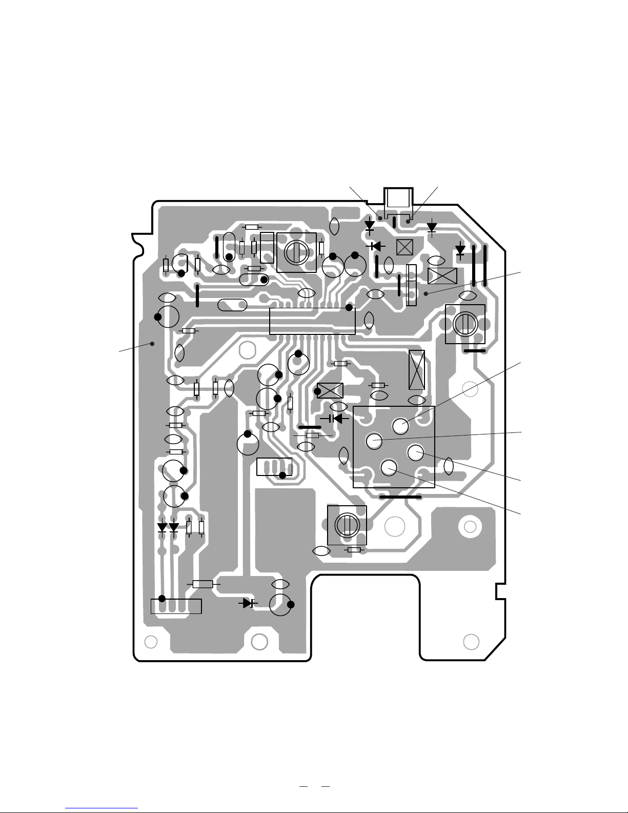
TUNER PCB TOP
PCB VIEWS
C28
C31
R3
CF3
IC1
C30
CF2
R4
Q1
C29
R16
L6
R15
R14
R21
C6
C5
C34
C19
C20
C6
C7
BF1
C21
R5
CF4
CF1
R12
C12
C27
D3
D4
CN1
CN2
D2
D1
C10
L5
C8
C11
L1
L4
R1
C4
C2
R8
L3
C14
R6
C3
D5
R2
C7
VC1
L2
R13
C18
C20
D8
C19
TUNER PCB
4754-520-2-91
CN3
R11
CN4
C16
C33
C32
R17
C24
R18
C13
R7
C25
C15
C17
C22
C26
R9
R10
C23
1
12
13
24
CN5
SW1
4754-520-2-92
SW PCB
SWITCH PCB TOP
30
Page 33

C327
C202
C102
C107
C108
R119
C302
C207
C208
C209
C113
C117
C109
C213
R206
R106
R215
R216
R217
R117
R116
R118
R218
R219
R115
R330
CN304
R204
R104
R205
R105
R107
R108
C311
FB302
FB303
FB301
FB300
FB304
C310
C09
R108
R211
R210
R320
D309
D308
R110
R202
C116
C216
R131
R231
R311
Q302
R111
R207
R209
R109
R103
R203
D100
R309
R308
R319
R304
D301
D300
R331
R126
R312
R313
R130
R323
R302 R212
R301
R214
R112
R113 R213
R114
R230
Q301
R127
R316
R128
R227
R224
R225
R125
R124
Q201
Q101
C201
C101
C200
C100
C305
C303
C306
C341
C307
C329
C215
C115
C119
C120
C112
R305
R303
R325
R324
Q302
Q331
Q103
Q104
Q203
Q204
C206
C211
C212
R226
R228
R307
R317
C217
C111
C304
C106
CN301
D200
C104
C105
C204
C318
C312
D303
R322
D304
C336
R102
C314
C313
FB305
FB306
IC301
D302
R310
IC302
C324
C220
C219
D201
R132
R223
R123
R232
CN305
R329
C222
C122
D101
CN303
CN302
C317
C205
C300
R314
C315
C322
C320
CN307
R321
C321
Q303
C323
C325
R326
IC300
R315
C316
C301
Q304
C319
R318
D307
D306
R328
D305
R327
C118
C328
C218
IC303
4754-500-0-91
AMP PCB
MC4754
MC4754JACK-PCB
4754-500-0-92
J301
R233
R133
WC305
WC306
WC307
AMP PCB TOP
JACK PCB TOP
31
Page 34

VR PCB TOP
32
R350
C352
SW352
SLEEP
C351
SW351
SOUND
C350
SW350
POWER
R351
D350
WC304
C359
C360
R358
C357
C358
R357
WC350
VR350
S353
R355
WC307
R352 R353
Q352
Q351
Q350
C356
C355
L351
L350
CN400
C354
MC-4754 VR PCB
4754-510-0-91
Page 35

PS PCB TOP
33
FUSE:2.5A/125V
FUSE:1.0A/125V
F401
F402
SK401
SW401
J401
C404
C403
C402
C401
D405
D404
D403
D402
C406
WC400
LF401
MC4754
PS PCB
4754-511-0-91
9
1
CN411
S103
S104
SW PCB A
4799-510-0-91
7
1
CN211
S101
2
1
3
SW PCB B
4799-510-0-92
SW A PCB TOP
SW B PCB TOP
Page 36

CD PCB TOP
34
DOOR PCB TOP
R815
R741
D702
D703
C724
C725
C736
C713
C710
R711
L701
R720
R807
L712
CN707
D714
C701
D701
C719
C711
R719
R802
C767
C744
C755
D706
D705
D704
C750
C853
X701
R818
CN708
2
1
CN7021
6
C840
C842
C773
C838
C771
C830
C828
C839
D709
D710
Q708
D708
L706
IC709
IC708
IC703
CN701
1
16
CN705
1
2
9
8
CN704
L716
L706
C827
L705
D707
C850
C832
C849
C814
X702
D780
C881
C781
C884
L719
D880
C704
1
8
CN703
C845
LAY DOWN
MC4754 CD PCB
4754-526-0-91
L718
13
1
CN706
L715
L714
L717
C834
C823
L707
R924
R925
R926
C824
L704
L703
L707
SW701
CN709
1
2
DOOR SW PCB
4754-526-0-92
Page 37

CD PCB BOTTOM
35
R946
Q710
Q709
R945
C837
R947
C843
R948
R949
TP812
C829
C841
TP741
TP742
R941
R940
C825
IC707
R939
TP811
TP807
TP806
TP805
TP808
TO801
TP809
JP900
TP850
R857
R832
TP810
TP942
TP941
TP938
C821
R913
TP939
TP803
TP940
TP944
TP802
TP936
R860
R770
TP937
TP943
JP903
TP739
C818
C820
C819
TP734
TP713
TP716
TP715
TP714
TP711
C846
C765
JP901
R820
R819
R810
R812
R813
TP728
C770
TP714
R814
C768
R811
R809
R808
C769
TP733
R943
R805
R804
R816
C772
TP732
JP906
C766
S706
TP730
TP731
TP935
TP934
TP727
C852
TP729
JP902
TP804
R930
R929
R928
R927
R912
JP910
JP909
JP908
R923
R922
R935
R933
R936
R937
R904
R905
R843
TP918
TP924
TP926
R856
TP903
TP873
TP874
R902
TP875
TP904
TP912
TP913
R844
TP914
Q706
Q707
R903
R934
TP925
TP867
TP814
TP813
TP778
TP921
R938
R833
TP773
R901
R878
R877
R876
R911
R917
R765
R771
C753
C754
R918
R874
R875
R869
R870
C817
R916
R900
R914
R915
R879
TP872
C813
C816
R858
C775
C778
C833
C779
C801
TP767
TP768
TP775
C777
C776
TP772
TP771
TP779
C822
TP774
R835
R836
R834
R837
R838
R919
R920
R921
R825
R827
R828
R826
R829
TP770
TP769
TP777
TP776
TP815
TP929
TP816
TP930
R932
R823
R931
R824
R830
R831
R863
R862
R864
R861
1
TP823
TP840
TP839
TP838
R847
TP837
R845
R848
R846
R849
R850
R851
R852
TP841
TP842
TP843
TP844
TP855
TP856
TP863
TP857
C809
C810
R867
R872
TP859
TP861
R777
R774
R773
R908
R871
TP856
R883
C885
C815
R873
R855
C805
C804
C803
C802
R854
R853
TP747
TP746
TP744
TP745
TP780
TP880
R884
R784
R801
R841
C764
TP749
R840
C847
C774
JP904
R783
R787
R887
Q780
Q880
C782
C882
R785
R885
C783
C883
R786
R886
C854
R778
C855
R747
TP755
TP754
R749
R751
R748
R782
R775
R780
R781
C760
C785
C758
C759
R776
JP907
C780
C756
C880
R881
C757
R882
R880
R772
JP905
R794
TP753
TP736
TP737
R768
R767R766
TP738
R764
C752
IC704
1
IC702
C761
C737
C746
C736
C762
R779
R750
C739
C738
C741
C740
R796
TP758
R797
R798
R795
TP757
TP740
R793
R740
C728
C726
R725
TP725
R944
C714
R942
C742
R752
R806
TP722
C743
R753
TP701
R756
R755
R754
R759
R758
R757
R803
R817
R760
R763
C751
R865
R746
C857
D715
C745
TP785
C747
C748
R859
R799
R701
R761
C749
R762
TP709
TP702
TP724
TP717
Q701
TP710
TP712
TP708
TP718
TP707
TP705
TP706
TP703
TP704
TP720
TP721
TP759
TP760
TP726
TP723
R745
R742
C732
R743
C733
C734
C735
R702
R744
C730
C731
R910
C729
R704
R703
R705
R709
R707
R706
R733
R737
R710
R708
R712
S701
R713
C712
S702
R718
R721
R722
R723
C851
R724
C718
C707
C706
C704
C703
R714
R716
R717
R715
C705
C708
C702
TP719
IC701
S704
S705
R738
R735
R739
R734
C727
R726
C856
R921
R728
R727
C720
R729
R730
R736
R731
R732
C721
C722
C723
Q702
R822
1
C715
C716
C717
S703
Q703
Page 38

R971
C970
C971
R972
R974
R973
C972
C973
C974
C963
C958
C964
C982
R950
C950
C984
C960
C961
C962
C951
C983
C981
C965
Q950
C994
R961
R964
R961
R963
R992
R993
R958
R957
D950
R956
C959
C966
C957
R951
R984
R983
1
5
6
23
24
29
30
35
36
54
55
60
R982
C956
C955
C954
R994
Q951
R960
C991
C990
C992
C993
R991
D954
R969
R962
D951
LCD950
CN950
SW991
PLAY/PAUSE
SW990
STOP
SW992
REC
SW993
MEMORY
LD950
SW994
PLAY
SW980
MBSR
MODE
SW981
DISPLAY
SW982
EDIT
SW983
DELETE
SW984
MD EJECT
SW973
B/SKIP
SW970
FR
SW972
ENTER
SW974
FF
SW971
F/SKIP
R955
R954
R953
R952
MC-4754 DISPLAY PCB
4754-515-0-91
DISPLAY PCB TOP
DISPLAY PCB BOTTOM
36
Page 39

BD PCB TOP
37
61
CN402
C401
C341
R418
R421
R417
R416
R415
R414
R419
R413
R412
R412
R404
R403
R407
C333
C162
+
+
+
+
+
+
+
+
+
+
+
CN401
CN402
9
1
1
3
2
4
C252
C405
C655
C406
Q501
FB303
FB304
FB305
CN302
3
1
L102
C334
L103
L612
L611
C653
RJ611
C612
R503
C553
FB501
R502
R501
L651
C551
C552
CN601
1
11
L604
L603
L602
L601
C654
IC601
C601
C602
C652
C651
C351
L301
X301
Q104
L401
C517
C501
C560
C507
C506
R323
C324
C317
C318
C319
C325
C323
R316
R313
C320
C134
C110
R303
R304
C303
R305
C302
C301
C305
R308
R310
C307
RJ101
C316
C315
C326
Q103
Q102
C352
C328
C327
C304
R328
R307
R309
C306
D301
R314
C308
C126
C125
C206
C340
R312
C309
R303
RJ102
R329
R320
R319
R318
R105
R123
R124
RT101
R315
R322
R317
C311
C136
C106
R115
R109
C137
C135
C101
C104
C103
C102
C310
R107
R106
R125
R104
C105
C312
C138
C128
C123
C108
C109
R321
R126
R127
R121
R122
R120
R103
C314
R331
C107
R128
C130
C139
C339
Q101D101
FB101
R101
R102
FB104
FB103
FB102
CN101
1
21
RJ104
C451
R409
C403
C402
R410
R411
R408
C251
CN201
7
1
C253
Q107
R166
IC102
1
7
14 8
C164
R164
R161
IC402
1
Q105
Q106
C163
D102
D103
CN301
1
2
BD PCB
4799-501-0-91
FB105
Page 40

BD PCB BOTTOM
38
C207
1
IC202
C336
R211
R212
C321R324
R327
R326
R325
C322
Q504
Q503
C558
C559
C512
R519
R518
C513
R521
R520
RJ601
RJ602
RJ603
RJ606
RJ607
RJ604
RJ605
C515
R515
R514
R517
R516
C510
C511
1
Q502
IC502
C562
R529
C404
C554
C555
C512
1
IC501
C557
C556
C516
D501
D502
R425
R513
R512
C506C514
R511
R510
C509
C332
C331
C338
C337
RJ103
C342
C165
C166
R406
R330
R114
C117
C118
C119
C124
C120
C122
C121
R119
R116
R113
R112
R111
R110
R108
C151
R526
R528
R527
R525
R405
C167
C330
C335
R208
R207
R163
R162
FB302
FB301
FB161
FB162
IC401
CR401
1
1
R301
R306
R311
R302
IC301
R204
R206
R203
C204
R205
C205
C203
C202
Q202
R202
R201
Q201
C254
C201
IC201
1
C111
R117
C112
C113
C114
C116
C129
C133
R118
C115
1
IC101
1
IC302
Page 41

39
WIRING DIAGRAM
Blue
Red
Red
Blue
T401
Power Transformer
PS PCB
1
3
WC400
CN709
2
1
DOOR SW PCB
CD Pickup
1
16
1
1
1
1
1
16
1
6
6
2
MOTOR PCB
CD MECHANISM
CN708
CN702
CN701
CN704
CN705
B
A
MD
CD
1
3
CN400
15
WC307
1
12
WC350
Shield
Red
White
Shield
Red
White
WC304
VR PCB
WC307
WC305
WC306
JACK A PCB
Speaker L chSpeaker R ch
4
1
AMP PCB
1
1
1
1
5
CN307
CN302 CN303 CN301
CN411
4
11
8
White
Red
Shield
Red
White
Shield
1
12
CN707
1
8
CN703
A
B
MD Record Head
2
1
MD Pickup
1
21
Disc Motor
Sled Motor
Red
Black
MD MECHANISM
SW B PCB
7
1
CN211
CN201
7
1
DISPLAY PCB
CN950
13
1
13
1
CN706
2
9
CD PCB
3
CN4
CN3
1
1
31
SW PCB
TUNER PCB
CN5
C99
C21
4
CN304
CN305
16
SW A PCB
BD PCB
CN301
CN102
CN101
CN402
CN401
1
1
1
1
1
2
2
9
1
11
CN601
4
1
6
21
Telescopic
Antenna
Page 42

40
IC LEAD IDENTIFICATION AND INTERNAL DIAGRAMS
IC1: TA2111N
1
12
24
13
AM
OSC
1 7532 6 10
12
11
24 23 20 19 17
AF
FM RF In RF GND
AGC V
CC
AM IF In FM IF In GND TUN LED ST LED QUAD
FM
OSC
AM
MIX
FM
RF
22 21
AM
DET
4
FM
MIX
AM IF FM IF
8 9
TUN
LED
ST
LED
ST/MO
FM/AM
Level
DET
FM
DET
AGC
FM
Mute
AF
BUFF
18
VCO
Divide
Decode
15
14 1316
AM RF
In
FM RF
Out
RF V
CC
FM OSC AM OSC AFC DET Out MPX In LPF2 LPF1 L-Out R-Out
AM Low
Cut
MIX Out
Page 43

IC101: AN8771NFH-V
1
16
17
32
3348
49
64
49
48
50
51
47
RF AMP
52
53
54
55
56
57
58
59
60
61
62
IV
IV
IV
63
64
46
43
42
41 40
39
38 37
IV
18Pin
ASOFSET
VCA
BPF
VCA
IV
IV
FBAL/
FOFSET
VCA
VCA
IV
IV
Mirror
Circuit
IV
IV
IV
IV
EQ
45
44
AGC
DSL
3TENV
21Pin
20Pin
Mode Control
36 35
34 33
NRFDET
OFTAMP
32
31
30
29
28
26
25
27
RFBDO
OFTR
23
24
ASBDO
22
21
19
18
20
17
TBAL/
TOFSET
1 2
3
94 5
6
7 8
10
12 14
11
TRCRS
13 15
16
41
Page 44

IC102: TC74VHCT541AFT
1
10
20 11
1920
1 2
18
103
17
4
16
5
15
6
14
7
13
8
12
9
11
V
CC
G2 Y1 Y2 Y3 Y4 Y5 Y6 Y7 Y8
G1 A1 A2 A3 A4 A5 GNDA8A7A6
IC201: AN8814SB-E1
114
1528
78
22 21
18 17 16 15 14 13 12 11
1/2
PV
CC
20
21
1/2
PV
CC
9
8
V
CC
Detect
Thermal
Protect
Circuit
7
6
4
5
3.3V
REG
1
2
22
24 25 26
Direction
Detect
Direction
Detect
27 28
Direction
Detect
Direction
Detect
FIN GND
V
REF
V
CC
2319
PGND 1 IN 1 PC 1
10
IN 2 PC 2 IN 3 IN 4 PGND 2
PV
CC
1 VO 1+ VO 1- VO 2+ VO 2- VO 3+ VO 3- VO 4+ VO 4- PVCC 2
42
Page 45

IC202: BA6289F
14
85
5
4
3
6
2
1
7
8
RIN
FIN
V
CC
V
REF VM
OUT1
OUT2
GND
Control
Logic
Driver
Driver
IC300, IC301: BA15218N
1 2
1 2 3 4 5 6 7 8
Out 1 -In 1 +In 1 GND +In 2 -In 2 Out 2 V
CC
18
43
Page 46

IC301: MN66614RC1
132
33
64
6596
97
128
35 33
TRNPLL
SYSPLL
31 59 58 60
Serial
Interface
3864 3961 37 9940
Digital In
Digital
Out
94
DINPLL
93
91
92
89
88
96,97
102
103
101
100
105
104
Digital
Audio
Interface
FS
Converter
ECC
SPM
Control
90
63
62
7
6
10
16
11
4
5
A/D
Converter
54
9
8
D/A
Converter
14131215262320241922212551119121120565055484947
ADIPDEM FMDEM
Digital
Servo
Processor
12344432829128127152 53
EFMMOD
EFMDEM
EFMPLL
65110~115
57
116
117
118
32
34
42
41
36
TS0
TS1
TS2
TS3
TS4
Chip Control
Data
Interface
87
86
85
74~68
80~77
External
DRAM
Control
126
108
107
ATRAC
Digital Signal
Processor
TRNPLLF
MDAIREF
SYSPLLF
SSCK
SELAD
SSDW
SSDR
CFSYNC
DIBUFO
DIBUFI
DIVCOI
DIPCO
DIULK
RX1
RX2
TX
RXDA
RCL
RSWSA
R384
CV384
CVDA
SDAR
SDAP
SWSA
SWS
SCL
FS384
MDISY
SCTSY
HFRP
VRB
VRT
GTK
GFC
3TMON
AVSS1
TE
FE
AS
XO
XI
NWE
NCAS
NRAS
RAD4~
RAD10
RDT0~
RDT3
EFMSEL
TCSEL
SYSFI
TRNFI
NRST
MONI0~5
VREF5
REFM
NREFM
PEFMS
PEFM1
PEFM2
EFMIREF
EFMPLLF
NRFDET
BDO
ADIP
VREFD
FOTRON
SPON
TVON
APCD
DR
NREC
125
TRCRS
OFTR
RFSWPG
FG
ASGAIN
FOFS
FBAL
TOFS
TBAL
ASOFS
TGAIN
FOD
TRD
TVD
SPD
STP
44
Page 47

IC302: TA8227P
12
1
3 4
6
5
8
2
7
11 10
Bias Circuit
Thermal
Shut Down
Protection
Circuit
9
Vcc1
Vcc2
B.S. 1 Out 1 Power GND
30 kΩ
45Ω
In 1 NF 1
Ripple
In 2 NF 2
30 kΩ
45Ω
Pre GND
(F In)
OUt 2
B.S. 2
Ch 1
Ch 2
16
12
7
IC302: KM44V1000DT-6
Refresh Timer
Refresh Control
Refresh Counter
Row Address Buffer
Col. Address Buffer
Data in
Buffer
Data out
Buffer
Control
Clocks
4
17
3
VBB Generator
10 20
V
CC
8
9
11
12
13
14
15
5
6
7
2
18
19
1
DQ0
DQ1
DQ2
DQ3
16
OE
A0
A1
A2
A3
A4
A5
A6
A7
A8
A9
RAS
CAS
W
Row Decoder
Sense Amps & I/O
Column Decoder
Memory Array
1,048,576 x 4
Cells
1 5 6 10
V
SS
20 16 15 11
45
Page 48

Vo
Vadj
GND
Vin
1 2 3 4
1
2
4
3
IC
IC303, IC708, IC709: PQ15RW11
46
Page 49

IC401: MN101C15F GA1
18
TXD, SBO0, P00
19
RXD, SBI0, P01
20
SBT0, P02
21
SBO1, P03
22
SBI1, P04
23
SBT1, P05
24
DK,BUZZER,P06
26RMOUT,TM0IO,P10
27
TM1IO, P11
28
TM2IO, P12
29
TM3IO, P13
30
TM4IO, P14
Port 0
Port 1Port 2Port 3
31
IRQ0,P20
32
SENS,IRQ1,P21
33
IRQ2, P22
34
IRQ3, P23
35
IRQ4, P24
25
RST, P27
36
SBO2, P30
37
SBI2, P31
Sub
Clock
Generator
System
Clock
Generator
CPU
MN101C00
ROM
96K Byte
RAM
4K Byte
A/D Convertor
Port 4
Watchdog Timer
Time Base Timer 5
External Interrupt
Port 5
15 16
XI
XO
13 12
OSC1
OSC2
14 11
VSSV
DD
17
MMOD
5655545352
P50, WE
P51, RE
P52, CS
P53, A16
P54, A17
57
58
59
60
61
62
63
64
P60, A0
P61, A1
P62, A2
P63, A3
P64, A4
P65, A5
P66, A6
P67, A7
Port 6
Port 7
Port 8
65
66
67
68
69
70
71
72
P70, A8
P71, A9
P72, A10
P73, A11
P74, A12
P75, A13
P76, A14
P77, A15
80
79
78
77
76
75
74
73
P80, LED0, D0
P81, LED1, D1
P82, LED2, D2
P83, LED3, D3
P84, LED4, D4
P85, LED5, D5
P86, LED6, D6
P87, LED7, D7
4544 4746 4948 5150 110
KEY0, P40
KEY1, P41
KEY2, P42
KEY3, P43
KEY4, P44
KEY5, P45
KEY6, P46
KEY7, P47
VREF+
VREF-
38
SBT2, P32
39
BR, P33
40
BG, P34
41
LDDMA, P35
42
STDMA, P36
43
DKDMA, P37
8 bit Timer 0
8 bit Timer 1
8 bit Timer 2
8 bit Timer 3
16 bit Timer 4
Port A
89 67 45 23
AN7, PA7
AN6, PA6
AN5, PA5
AN4, PA4
AN3, PA3
AN2, PA2
AN1, PA1
AN0, PA0
Serial Interface 0
Serial Interface 1
Serial Interface 2
Data Automatic Transfer
1
20
21
40
41
60
61
80
47
Page 50

IC402: BR93LC46F-E2
14
85
6Bit
6Bit
Instruction
Register
Dummy Bit
Add
Buffers
Data
Register
R/W
AMPS
Add
Decorder
Write Disable
High
Voltage
Generator
1024Bit
EEPROM
Array
Detect Supply Voltage
Instruction Decode Control
and
Clock Generation
3
4
5
6
16Bit
16Bit
CS
SK
DI
DO
2 7
V
CC
GND
48
Page 51

IC501: PCM3003E-T2
4
6
21
19
3
5
20
91413212324
22
8
12
11
15
66
18
17
7
10
(+)
(-)
(+)
(-)
Analog
Front-end
Circuit
Reference
Analog
Front-end
Circuit
Analog
Low-pass
Filter
Analog
Low-pass
Filter
Power Supply
Multi-level
Delta-sigma
Modulator
Multi-level
Delta-sigma
Modulator
Delta-sigma
Modulator
Delta-sigma
Modulator
Decimation
&
Low Cut Filter
ADC
Decimation
&
Low Cut Filter
Interpolation
Filter X8
Oversampling
Interpolation
Filter X8
Oversampling
DAC
Clock
Reset and
Power
Down
Mode
Control
Interface
Serial
Interface
VINL
VREF1
VCOM
VREF2
VINR
VOUTL
VOUTR
LRCIN
BCKIN
DIN
DOUT
20BIT
DEM0
DEM1
/PDAD
/PDDA
AGND2 V
CC
2 AGND1 VCC1 VCC1 DGND VDD SYSCK
1
12
24
13
49
Page 52

IC502: BA4510F-E2
+In 2-In2Out 2V
CC
Out 1 -In 1 +In 1 V
EE
2
1
14
8
5
1 2 3 4
5678
IC601: UPC29M33T-E1
1 2 3
4
Start-up
Circuit
Reference
Voltage
Thermal
Shut Down
Error
AMP.
Drive
Circuit
Saturation
Protection
Over Current
Protection
Safe Operating
Area Protection
1
3
2
4
Input
Output
GND
50
Page 53

IC701: CXA2542AQ
36
25
37
48
1
13
24
12
IFB1
IFB2
IFB3
IFB4
IFB5
IFB6
TOG1
TOG2
TOG3
TOG4
36
37
38
35 34
Laser Power
Control
APC
V
CC
33
29
39
40
BAL1
BAL2
BAL3
BAL4
41
42
43
44
45
46
47
48
Tracking
Phase Compensation
V
CC
13
1 2 3 4 5 6 7 8 9 10 11 12
14
Focus
Phase Compensation
FSET
15
16
ISET
17
18
20
19
22
23
24
2528
IIL
TTL
IIL
TTL
IIL
TTL
V
CC
V
CC
FOK
V
EE
Level S
V
CC
V
EE
V
EE
MIRR
FO. Bias
Window
COMP.
FOH
FOL
TGH
TGL
BALH
BALL
ATSC
TZC
FZC
LDON
MIRR
TGFL
LPC
LPCL
DFCT2
CC1
IIL Data Register
Input Shift Register
Address Decoder
Sens Selector
Output Decoder
DFCTO IFB1-6
BAL1-4
TOG1-4
FS1-4 TG1-2 TM1-7 PS1-4
V
EEVEE
TM5
TM2
TM6
TM4
TM3
TM7
TG2
V
cc
V
EE
FS1
FS2
V
cc
V
cc
V
cc
V
cc
V
cc
V
EE
V
EE
V
EE
V
EE
V
EE
RF
Summing AMP.
FE AMP
PD1 IV AMP
PD2 IV AMP
F IV AMP
E IV AMP
TGFL
Track Gain
E-F
Balance
Window
COMP.
ATSC
Window
COMP.
TZC COMP.
FZC COMP.
DFCT
TM1
TG1
FS4
DFCT
FEO FZC VC TDFCT TZC ATSC LPFI TEO V
EE
E F PD2
PD1 PD LD RFTC RF M RF O RF I CP CB CC1 CC2 FOK
FEI FDFCT FGD FLB FE O FE M SRCH TGU TG2 FSET TA M TA O
Window
COMP.
SL P SL M SL O ISET V
CC
CLK XLT DATA XRST C.OUT SENS1 SENS2
21
XDFCT2
27
30 26
31
V
EE
V
CC
V
EE
V
CC
32
V
EE
V
CC
INT
51
Page 54

IC702: CXD3009Q
1
20
21
40
41
60
61
80
PWM PWM
65
AOUT1AIN1
66
67767574141312 532145595857
48
30
29
38
52
33
31
36
37
11
18
10
1716159876 22
XTSL
VPCO
VCKI
V16M
VCTL
XUGF
GFS
EMPH
WFCK
C2PO
LRCK
PCMD
BCK
EMPHI
LRCKI
PCMDI
BCKI
SYSM
XTAO XTAI LMUT RMUT XRST TEST TES1
DATO
XLTO
CLKO
SENS
DATA
XLAT
CLOK
SPOA
SPOB
XLON
SCOR
SBSO
EXCK
SQSO
SQCK
MDP
PWMI
DOUT
LOUT2
AIN2
AOUT2
LOUT1
CNIN SEIN FOK CLTV PCO FILI FILO XPCK BIAS ASYO ASYI RF C4M
Error
Corrector
16K
RAM
Servo
Auto
Sequencer
CPU
Interface
Digital
CLV
Digital
Out
Over Sampling
Digital Filter
3rd-Order
Noise Shaper
Timing
Logic
Serial-In
Interface
D/A
Interface
EFM
Demodurator
OSC
Clock
Generator
Asymmetry
Corrector
Digital
PLL
Sub Code
Processor
27 282551 26 47 49 54 56 55 40 4243413950 6244
3
71
70
2
79
23
24
35
52
Page 55

IC703: BA6898S
1
16
17
32
Level Shift
28 27
Level Shift
22 2129 2026 25
Level Shift
8 9 10
Level Shift
6 754321
V
CC
2332 18 173031
V
CC
1924
11 12 16151413
Driver Mute
Regulator
Bias T. S. D.
Monitor
Regulator
50K
50K
10K
10K
100
10K
10K
13.3K
13.3K
13.3K
13.3K
D. BUF
D. BUF
D. BUF
D. BUF
D. BUF
D. BUF
D. BUF
D. BUF
OP-AMP
T. S. D.
SUB VCC IN4' IN4 OUT4-A OUT4-B NC OPIN-B OPOUT GND OUT3-B OUT3-A IN3 IN3' GND NC
NC V
CC
V
REF
IN IN1' IN1 OUT1-A OUT1-B GND OUT2-B OUT2-A IN2' RESET REG-B REGOUT MUTE SUB
T. S. D. : Thermal shut
down
D. BUF: Drive buffer
10K
BIAS
53
Page 56

IC704: CXP740056-105Q
PF5/AN9
PF6/AN10
PF7/AN11
PK3/SCK0
PK4/SO0
PK5/SI0
PK6/CS0
EXTAL
XTAL
V
SS
RST
PK7/TO1
PH0
PH1
PH2
PH3
PH4
PH5
PH6
PH7
PC5
PC4
PC3
PC2
PC1
PC0
PB7/SI2
PB6/SO2
PB5/SCK2
PB4/TO2
PB3
PB2
PB1
PB0
PJ7
PJ6
PJ5
PJ4
PJ3
PJ2
PJ1
PJ0
PD7
PD6
PD5
PD4
PD3
PD2
PD1
PD0
50
49
48
47
46
45
44
43
42
41
40
39
38
37
36
35
34
33
32
31
1234567891011121314151617181920212223242526272829
30
8079787776757473727170696867666564636261605958575655545352
51
81
82
83
84
85
86
87
88
89
90
91
92
93
94
95
96
97
98
99
100
PI5/SCK1
PI4/INT1/CS1
PI3/TO0/ADJ
PI2/NMI
PI1/RMC
PK2/TEX
PK1/TX
V
SS
V
DD
NC
PA7
PA6
PA5
PA4
PA3
PA2
PA1
PA0
PC7
PC6
PI6/SO1
PI7/SI1
PE0/INT0
PE1/INT2
PE2PWM0
PE3/PWM1
PE4
PE5
PE6
PE7
PG0/T
X
D
PG1/R
X
D
PG2/EC0
PG3/EC1
PG4/EC2
PG5/INT3
PG6/INT4
PG7/CINT
AN0
AN1
AN2
AN3
PF0/AN4
PF1/AN5
PF2/AN6
PF3/AN7
AV
DD
AC
REF
AVSSPE4/AN8
A/D Converter
UART Receiver
URAT Transmitter
UART Baud Rate
Generator
12 Bit PWM Generator 0
12 Bit PWM Generator 1
Remocon In
Interrupt Controller
FIFO
Serial Interface Unit
(CH2)
NMI
INT0
INT1
INT2
INT3
IN
T
4
2
2
2
12
2
6
8
Prescaler/
Time Base
Timer
32 KHz
Timer/
Counter
SPC700
αα
αα
α II
CPU Core
ROM
56K/96K/120K
Bytes
RAM
4096 Bytes
AN0~AN11
R
X
D
T
X
D
PWM0
PWM1
RMC
SI2
SO2
SCK2
ADJ
AVDDAV
REF
TEX
TX
EXTAL
XTAL
RST
V
DD
V
SS
Clock
Generator/
System
Control
PA0~PA7
PB0~PB7
PC0~PC7
PD0~PD7
PE0, PE1
PE2~PE7
PF0~PF7
PG0~PG7
PH0~PH7
PJ0~PJ7
AV
SS
Port APort BPort CPort DPort EPort FPort GPort HPort IPort J
PI1~PI7
Port K
2
5
PK1, PK2
PK3~PK7
16 Bit CAPTURE
Timer/Counter 4
TO2
CINT
EC2
EC0
TO0
8 Bit Timer/Counter 0
8 Bit Timer 1
EC1
TO1
8 Bit Timer/Counter 2
8 Bit Timer 3
Serial
Interface
Unit (CH0)
Buffer
RAM
CS0
SI0
SO0
SCK0
Serial
Interface
Unit (CH1)
Buffer
RAM
CS1
SI1
SO1
SCK1
8
8
8
8
8
8
7
8
54
Page 57

IC707: S-80727AL-AQ-T1
2V
DD
VSS3
Parasitic Diode
1
OUT
1 2 3
55
Page 58

IC950: EOC62A3BF1N
Stopwatch
Timer
FOUT
& Buzzer
Output Port
Clock
Timer
Power
Controller
Serial Interface
OSC
RAM
96 words x
4 bits
LCD Driver
26 SEG x 4 COM
Interrupt
Generator
Input Port
I/O Port
System Reset
Control
Core CPU E0C6200B
ROM
1,536 words x 12 bits
RESET
43
56
55OSC1
OSC2
54
57
53
COM0
SEG0
V
DD
V
D1
V
SS
V
C1
CA
49
48
R00
R01
R02
33
34
35
36
37
P00
P01
P02
P03
TEST
K00
3
4
6
COM3
COM2
COM1
32
~
~
SEG25
1
60
58
59
2
V
C2
V
C3
CB
7
50
51
R03
~
44
~
47 K03
24
35
1
23
36
54
55
60
5
6
5
30
29
56
Page 59

1 432
GND
+5V
R ch
L ch
CN3
!
R11
JP
D7 RB721Q
D6 RB721Q
R20
100K
R19
100K
CF3
C32
1/50V
C33
1/50V
C24 1200P
C25 1200P
C22 0.012
C23 0.012
R9 22K
R10 22K
SW1
BAND SW
C19
470/10V
13
12
8
17
9
16
10
15
11
14
3
4
5
6
7
22
21
20
19
18
1
2
23
24
C31
100/16V
C28 0.022
CF2
10.7MHz
JP9
L6
R4
JP
R5 330
CF1
455KHz
C30
0.047
QUD
SL
TL
GND
FIF
AIF
VCC
C12 4.7/50V
AGC
MIX
C27
0.47/50V
GND
AM-IFT
FIN
C11
22P
JP6
C9
15P
L5
FM ANT
NP
C10 33P
CN2
D3
1SS133
D4
1SS133
ANT1
Rod Antenna
C18 100P
R13 100K
PVC AM-OSC
R3 10
C5
8P (4-12P)
C13
1000P
L2
AM OSC
PVC AM-ANT
PVC FM-OSC
PVC FM-RF
Rch
Lch
R7 3.3K
C16
1/50V
C17 0.1/50V
C14 10/50V
C15 0.1/50V
FOS
VCC
FOT
AIN
R1 JP
FM-RF
L4
C4
C26 0.022
C99 22P
C21
1000P
To Speaker
To VR Unit
CN1
AM Loop
Antenna
C8 0.022
FM OSC
L3
C2
R8 2.2K
C3
5P
L1
AM ANT
C6
0.022
JP2
JP1
Notes:
1. All resistance values are in ohms (k=1000 ohms, M=1000 kohms).
2. All capacitance values are In µF (P=10
-6
µF).
3. All resistors are 1/6 watt, unless otherwise specified.
* Parts marked with are of importance in respect to the safety.
Use the specified type without fail
* NP is no insert parts.
!
SCHEMATIC DIAGRAMS
TUNER
22P
(18-27P)
22P
(18-27P)
AM
FM-MO
FM-ST
To AMP
AM 5.0V 5.0V 5.0V 5.0V 5.0V 0.9V 1.1V 0.7V 5.0V 3.8V 1.3V 1.3V
FM 5.0V 5.0V 5.0V 5.0V 5.0V 0.3V 1.1V 0.7V 3.8V 5.0V 1.3V 1.3V
AM 0V 0V 1.0V 5.0V 0V 5.0V 4.4V 5.0V 0V 0V 0V 4.5V
FM 0.8V 0V 0.3V 4.9V 0V 5.0V 4.4V 5.0V 0V 0V 0V 4.3V
IC1
TA2111N
57
Page 60

Notes:
1. All resistance values are in ohms (k=1000 ohms, M=1000 kohms).
2. All capacitance values are In µF (P=10-6 µF).
3. All resistors are 1/6 watt, unless otherwise specified.
58
1
2
3
4
5
6
7
8
NC
CD R
A GND
CD L
BBS
AF MUTE
SURROUND
D GND
CN301
to CD
R207 68K
R107 68K
4
3
2
1
TU L
TU R
TU 5V
GND
CN302
to Tuner
FB300 FERRITE
FB301 FERRITE
11
10
9
8
7
6
5
4
3
2
1
REC IN (L)
MD OUT L
A GND
REC IN (R)
MD OUT R
D GND (M)
D GND (H)
SYS GND
M+5V
G+5V
+5V (MDLSI)
CN303
to MD
R109
82K
R209 82K
D100
RB721
D200
RB721
2
413
2
4
3
1
9.2
5.0
2.6
0
C104
4.7/50V
C204
4.7/50V
R108
22K
R208
22K
FB302 0
FB303 0
FB304 0
FB305 FERRITE
D303
1SS133
C312
1000/10V
C313
100/10V
R320
10K
R322
2K
R321
1.8K
IC303
PQ15RW11
C314
330/16V
FB306 FERRITE
C316 47/16V
R323 10K
R202 33K
R102 33K
R111 1K
R211 1K
C205
1/50V
R113
47K
R114
470K
R214
470K
R213
47K
R112
220K
R212
220K
C300
100/10V
R301
4.7K
R302
4.7K
C301 100/10V
OUT1
-IN1
+IN1
VEE
+IN2
-IN2
OUT2
VCC
IC300 BA15218N
1234567
8
0
0.6
0 0
0
0.6
8765432
1
VCC
OUT2
-IN2
+IN2
VEE
+IN1
-IN1
OUT1
IC301 BA155218N
C209 10P
R219 10K
C212
0.1/50V
C112
0.1/50V
C109 10P
R119 10K
R117 10K
R116
470K
R118
1.5K
C107 0.082
C108 0.047
C207 0.082
C208 0.047
R216
470K
R218
1.5K
R217 10K
R305 10K
C304
47/16V
C303
470/10V
C302 0.1
R304
9.1K
R115
4.7K
C106
4.7/50V
R215
4.7K
C206
4.7/50V
R303
100(1/4W)
R104
560K
C100
4.7/50V
C101
1/50V
C102
1000P
Q101
2SD1302
C
B
E
R103
22K
R105
2.2K
R205
2.2K
R203
22K
C201
1/50V
C202
1000P
C200
4.7/50V
R204
560K
R206
2.2K
R106
2.2K
C327
470/10V
R330
100(1/4W)
R309
10K
R307
2.2K
R310
100K
C329
22/16V
Q302
2SC3330
E
C
B
C
E
B
Q301
2SD1302
R311
18(1/4W)
C328
47/16V
65432
1
Lch VI
Rch VI
GND
Rch VO
Lch VO
GND
CN304
to Volume
65413321
789
14
101112
IN1
NF1
PREGND
PWGND
BS1
OUT1
VCC2
IN2
NF2
RPL
PWGND
BS2
OUT2
VCC1
IC302
TA8227P
C213 1000P
R226 47K
R126 47K
C113 1000P
R225 4.7K
R125 4.7K
R124 220K
R224 220K
Q203
2SC2120-Y
Q103
2SC2120-Y
R128 1K
R228 1K
R127 100K
R227 100K
Q204
2SD1302
C
B
E
B
E
C
B
E
C
Q104
2SD1302
C
B
E
C211
4.7/50V
C111
4.7/50V
C215
4.7/50V
C115
4.7/50V
C116
2200P
C216
2200P
R130
2.2K
R230
2.2K
R231
180
C218
47/16V
C217
120P
C219
100/16V
C220
1000/10V
C222
0.15
R232
2.2(1/4W)
R132
2.2(1/4W)
C122
0.15
C120
1000/10V
C117
120P
C118
47/16V
R131
180
C307
470/10V
C119 100/16V
C324
470/16V
R329
0
D101
1SS133
D201 1SS133
R123
220K
R223
220KC306
1/50V
R319
22K
R317
100K
R331
100K
R318
100K
Q331
2SC3330
B
E
C
0
0
0.6
C341
0.47/50V
R316
2.2M
C308
22/16V
R312
10K
D302
1SS133
D300 RB721
D301 RB721
R314
47
R315
2.2K
R313
4.7K
4
3
2
1
CN305
CON4
1
2
3
4
5
CN307
VCC9V
DC9V
GND
TUNER9V
MD9V
to VR
3
2
1
GND
DC9V
GND
WC400
to VR
5.2
R325
330(1/4W)
C317
470/10V
C318 00.22
D304 5.1B
C325
470/10V
D305
3.9B
C319
1/50V
R327
120K
2.4
1.8
9.9
R326
100K
D306
1SS133
D307
5.6B
7.3
10.4
CE
Q303
2SB1655
B
C
Q304
2SC3330
B
E
R328
1K
C320 0.022
C321 330/16V
C315
1000/16V
C322 0.022
C323 2200/16V
D308 1T4 D309 1T4
R324 10K
3
4
124
3
1
2
1
2
1
2
C406
4700/16V
D402 1N5401
D404 1N5401
D405 1N5401
D403 1N5401
C401 0.022 C403 0.022
C402 0.022 C404 0.022
F401
FUSE:2.5A/125V
T401
TRANS
INININ
IN
LF401
JUMPERX2
F402
JUMPER
21J401
AC IN
EU: AC230V/50Hz
HK: AC220V/50Hz
4
3
2
1
WC305
CON4R
J301
H. P
R233 270
R133 270
1 GND
5 RIN
4 SPR
3 H. PR
2 H. PL
6 SPL
7 LIN
1
2
2
1
1
2
2
1
WC306
SPL
WC307
SPR
LchA
SP
RchA
SP
AMP UNIT
H/P JACK UNIT
PS UNIT
C305
100/10V
R308
10K
E
C
B
C105
1/50V
2
1
1
2
Q201
2SC1302
AMP
V
Voltage check position
Power on CD stand-by
Power on tuner stand-by
Power on MD stand-by
V
V
Page 61

TP724
C734
0.01
R742
15K
TP717
Q701
2SA1037K
C736
1/50V
C713
100/6.3V
R744
18K
D701
1SS133
C701
100/
6.3V
L701
10uH
TP701
TP708
TP709
TP710
TP711
TP712
1
2
3
4
5
6
7
8
9
10
11
12
13
14
15
16
CN701
TO
MECHA
FFC
VC
VCC
E
D
A
B
C
F
GND
LD
R701
JP
TP702
TP703
TP704
TP705
TP707
TP706
R745
1M
R702
10
R703
68K
R704
68K
R705
68K
R706
68K
F
E
I
1
F
D
F
C
T
2
F
G
D
3
F
L
B
4
F
E
O
5
F
E
M
6
S
A
C
H
7
T
G
U
8
T
G
2
9
F
S
E
T
1
0
T
A
M
1
1
T
A
O
1
2
SL-P
13
SL-M
14
SL-O
15
ISET
16
VCC
17
CLK
18
XLT
19
DATA
20
XRST
21
C-OUT
22
SENS1
23
SENS2
24
F
O
K
2
5
C
C
2
2
6
C
C
1
2
7
C
8
2
8
C
P
2
9
R
F
I
3
0
R
F
O
3
1
R
F
M
3
2
R
F
T
C
3
3
L
D
3
4
P
D
3
5
P
D
1
3
6
PD2
37
F
38
E
39
VEE
40
TEO
41
LPFI
42
ATSC
43
TZC
44
TDFCT
45
VC
46
FZC
47
FEO
48
IC701
CXA2542AQ
R707
68K
R708
68K
D702
1SS133
D703
1SS133
C729
0.068
R743
2.2K
C733
0.1
C730
0.01
C732
15P
R910
220K
R793
1K
C731
0.033
TP760
R749
22K
R750
22K
R751
22K
TP754
TP755
TP757
TP752
TP751
R747
22K
R748
22K
FOK
TP753
SENS2
SENS1
CLK
XRST
XLT
DATA
SCOR
SQSO
SQCK
MUTE
C_GND
C850
220/6.3V
R746
JP
TP758
R798
1K
R797
1K
R796
1K
R795
1K
R779
1K
C763
0.047
TP740
R752
JP
R753
JP
C742
0.1
R944
47K
R740
1K
R737
3.9K
C726
0.015
C727
0.1
R738
120K
TP723
R736
56K
1
2
S702
SHORT/L
TP719
TP720
C704
0.022
C712
0.1
C705
0.01
1
2
S701
SHORT/L
TP718
VR
PD
FO+
TR+
TRFO-
R712
100K
R713
150K
C702
0.033
C703
0.033
R714
100K
C706
4700P
B
C707
4700P
B
TP721
TP722
R723
JP
R721
JP
C708
0.1
C715
0.1
R942
10K
R722
330K
C716
0.1
C717
0.1
R715
100K
R716
100K
C714
2200P
R718
18K
Q703
2SC2412K
R729
510K
R727
JP
C719
4.7u
50V
R725
JP
R730
100K
C721
0.015
C720
0.047
R733
82K
R734
47K
R822
10K
R757
10K
R758
3.3K
R759
3.3K
C743
0.01
C725
0.1/50V
C745
0.047
R806
4.7K
C767
3.3u
50V
C724
3.3/50V
V
S
S
1
L
M
U
T
2
R
N
U
T
3
S
Q
C
K
4
S
Q
S
O
5
S
E
N
S
6
D
A
T
A
7
X
L
A
T
8
C
L
O
K
9
S
E
I
N
1
0
C
N
I
N
1
1
D
A
T
O
1
2
X
L
T
O
1
3
C
L
K
O
1
4
S
P
O
A
1
5
S
P
O
B
1
6
X
L
O
N
1
7
F
O
K
1
8
V
D
D
1
9
V
S
S
2
0
VPCO
25
VCKI
26
VI6M
27
VCTL
28
PCO
29
FILO
30
FILI
31
AVSS
32
CLTV
33
AVDD
34
RF
35
BIAS
36
ASYI
37
ASYO
38
LRCK
39
LRCKI
40
MDP
21
PWMI
22
TEST
23
TES1
24
P
C
M
D
4
1
P
C
M
D
I
4
2
B
C
K
4
3
B
C
K
I
4
4
V
S
S
4
5
V
D
D
4
6
X
U
G
F
4
7
X
P
C
K
4
8
G
F
S
4
9
C
2
P
O
5
0
X
T
S
L
5
1
C
4
M
5
2
D
O
U
T
5
3
E
M
P
H
5
4
P
M
P
H
I
5
5
W
F
C
K
5
6
S
C
O
R
5
7
S
B
S
O
5
8
E
S
C
K
5
9
V
S
S
6
0
VDD
61
SYSM
62
AVSS
63
AVDD
64
AOUT1
65
AZN1
66
LOUT1
67
AVSS
68
XVDD
69
XTAL
70
XTAO
71
XVSS
72
AVSS
73
ROUT2
74
AIN2
75
AOUT2
76
AVDD
77
AVSS
78
XRST
79
VDD
80
IC702
CXD3009Q
C744
1/50V
R756
1M
R755
100K
R754
1K
C737
0.1
R782
12K
R781 12K
R780 12K
R777
JP
R783
JP
R785
100K
C761
0.1
C780
150P
R784
10K
R776
820
C760
22P
R787
100K
R778 100
C785
680P
C782
C847
560P
0.1
C781
10/16V
1
2
3
4
5
6
7
8
CN703
TO AMP
TP749
TP780
Rch
LINE
D780
1SS133
1SS133
C847
0.1
L719
FBA04HA600
C784
TP744
TP745
TP746
TP747
TP880
BBS
SOUND
AMUTE
Lch
GND
BBS
SOUND
AMUTE
D GND
D880
C884
10/16V
10/16V
R882
12K
R880
12K
R881 12K
R774
JP
R775
1M
R885
100K
R883
JP
C757
0.1
C758
0.1
X701
16.9344MHz
C880
150P
R884
10K
C759
22P
R887
100K
C885
680P
C882
560P
C881
10/16V
TP735
R762
100K
R763
10K
C751
0.01
R761
1M
1
2
S706
SP
C747
4700P
C746
1500P
C749
220P
Q702
DTA114TK
1
2
S705
SL
TP726
1
2
S704
TR
R724
150K
C711
100/
6.3V
C710
100/
6.3V
C718
C857 0.047
100P
TP714
TP715
1
2
S703
FO
C846
0.1
C755
100/6.3V
C748
0.1
R760
JP
R770
JP
C750
4.7/50V
D715
5.1B
C752
0.1
R764
JP
TP737
R771
JP
C756
0.1
R772
47K
R766
330
R794
1K
R865
BK2125HS601
TP736
TP741
C773
100/6.3V
R841
100K
R773
100
C845
220/16V
C849
220/6.3V
LMUTE
SVCC
PVCC
CD_GND
DI_GND
CDVCC
R860
BK2125HM601
TP742
R840
10K
R859
BK2125HS601
C771
1000/16V
C772
0.1
R820
15K
TP725
TP761
TP762
R804
10K
R803
12K
R816
22K
NC
1
VCC
2
VREF
3
VIN_1
4
VIN1
5
OUT1+
6
OUT1-
7
GND
8
OUT2-
9
OUT2+
10
VIN_2
11
RESET
12
REG_B
13
REGOUT
14
MUTE
15
SUBGND
16
NC
17
GND
18
VIN_3
19
VIN3
20
OUT3+
21
OUT3-
22
GND
23
OPOUT
24
OPIN-
25
NC
26
OUT4-
27
OUT4+
28
VIN4
29
VIN_4
30
VCC
31
SUBGND
32
IC703
BA6898S
TP730
TP716
TP713
SP
TP732
TP729
1
2
3
4
5
6
CN702
TO MECHA
TP734
TP727
SP
SL
SL
PSET
PSET
TP731
TP733
TP763
TP764
R805
JP
R943
JP
TP728
R809
10K
1
2
CN704
TO MD
TP738
TP739
DOUT
D/GND
R767
JP
R768
L720
JP
PLP3216S551SL2T1
59
Notes:
1. All resistance values are in ohms (k=1000 ohms, M=1000 kohms).
2. All capacitance values are in µF (P=10-6 µF).
3. All resistors are 1/10 watt, unless otherwise specified.
CD 1/2
Page 62

R832
470K
TP816
TP815
TP930
TP929
R838
47K
R837
47K
R836
47K
R835
47K
R834
47K
R833
47K
R863
47K
R862
47K
R861
47K
BBS
C GND
SOUND
AMUTE
LMUTE
SCOR
XRST
SENS2
SENS1
XLT
CLK
DATA
TP837
TP838
TP839
TP840
TP841
TP842
TP843
R855
47K
R854
47K
R853
47K
R845
1K
R846
1K
R847
1K
R848
1K
R849
1K
R850
1K
TP823
R831
1K
R830
1K
R829
1K
R828
1K
R827
1K
R826
1K
R825
1K
L714
10uH
L717
10uH
1
2
3
4
5
6
7
8
9
10
11
12
13
CN706
TO FRONT
TP767
TP769
TP770
TP768
TP771
TP772
TP773
TP774
TP775
TP776
TP777
TP778
LCD/DB3
LCD/DB2
LCD/DB1
LCD/DB0
LCD/E
LCD/CLK
KEY0
VCC
GND
DC9V
K GND
L715
FBA04VA600
L718
FBA04VA600
TP779
TP801
TP802
KEY2
KEY1
GND
PWR/SW
1
2
3
4
5
6
7
8
9
10
11
12
CN707
TO VOL
DC9V
TP850
C833
0.1
C834
100/6.3V
R928
47K
R929
47K
R930
47K
R823
1K
R9321KR931
1K
123344556677889
1
0
1
0
1
1
1
1
1
2
1213141516171
8
1
9
1
9
2
0
2
0
2
1
2
1
2
2
2223242526272
829
3
0
31
31
32
32
33
33
34
34
35
35
36
36
37
37
38
38
CLKSHIFT
39
RST
40
VSS
41
XTAL
42
EXTAL
43
BL/CONT
44
CD/SQSO
45
46
46
CD/SQCK
47
48
48
DOOR/SW
49
50
50
5
1
5
1
A
V
S
S
5
2
A
V
R
E
F
5
3
A
V
D
D
5
4
5
5
5
5
5
6
5
6
5
7
5
7
5
8
5
8
K
E
Y
3
5
9
K
E
Y
2
6
0
K
E
Y
1
6
1
K
E
Y
0
6
2
T
E
M
P
D
E
T
6
3
C
D
/
S
C
O
R
6
4
M
D
/
C
T
S
6
5
M
D
/
P
D
O
W
N
6
6
M
D
/
R
E
S
E
T
6
7
M
D
/
R
T
S
6
8
M
D
/
R
X
D
6
9
M
D
/
T
X
D
7
0
7
1
7
1
7
2
7
2
7
3
7
3
7
4
7
4
7
5
7
5
F
A
N
/
C
O
N
T
7
6
7
7
7
7
P
S
D
E
T
0
7
8
P
S
D
E
T
1
7
9
M
D
/
M
U
T
E
8
0
81
81
82
82
83
83
PWR/KEY
84
85
85
86
86
87
87
VSS
88
VDD
89
90
90
F/TUNER
91
F/MD
92
F/CD
93
94
94
95
95
BBS
96
SURROUND
97
98
98
99
99
100
100
IC704
CXP740056
TP844
R851
1K
TP859
R870
1K
CD_GND
SVCC
PVCC
SQCK
MUTE
FOK
SQSO
CDVCC
DI GND
R867
1M
C809
15P
C810
15P
X702
12MHz
TP856
TP857
TP861
TP863
TP855
TP925
TP926
C823
100/
6.3V
C822
0.1
TP921
R926
1K
R925
1K
R924
1K
R923
1K
TP918
R927
47K
R938
B2125HS601
TP924
TP867
L712
FBA04VA600
L713
FBA04VA600
D707
5.1B
D714
JP
TP803
TP804
TP805
TP806
TP807
TP808
TP809
TP810
TP811
CD9V
VCC
F/MD
F/CD
DC9V
KEY3
F/TUNER
D-GND
PS/CONT
R936
22K
Q707
2SC2412K
R937
56K
TP813
TP913
TP914
R844
1K
Q706
2SC2412K
R934
10K
R935
100K
R933
47K
L707
FBA04VA600
C824
22/6.3V
TP912
TP904
R843
1K
L702
100uH
L703
100uH
TP854
R874
47K
C816
0.1
C813
0.1
R871
22K
R875
1K
R872
1K
TP934
TP935
SW701
DOOR SW
1
2
CN708
TO SW
1
2
CN709
TO CD
GND
DOOR
GND
DOOR
TP936
1
2
3
4
5
6
7
8
9
CN705
TO MD
FFC
CPU GND
TEMP DET
CTS
P DOWN
S RESET
RTS
TXD
RXD
MD MUTE
L716
FBA04VA600
TP937
TP938
TP939
TP940
TP941
R917
47K
R916
47K
R915
47K
R914
47K
R913
47K
TP942
TP943
R912
47K
R911
47K
R905
JP
TP944
R908
22K
R904
JP
R876
1K
R901
1K
R879
1K
R900
1K
R869
1K
TP872
R918
100K
R919
100K
R920
100K
R921
100K
R903
47K
R922
1K
L704
100uH
R902
1K
L705
10uH
R939
47K
1
2
3
IC707
S-80727AL-AQ-T1
C828
1/50V
R858
BK2125HS601
R857
BK2125HS601
L706
10uH
VIN
1
VO
2
VADJ
4
G
N
D
3
IC708
PQ15RW11
TP812
R940
470
TP875
TP874
TP873
R941
1.8K
C829
0.1
C830
220/
16V
TP814
C825
0.1
C827
100/6.3V
TP903
R856
1K
R877
1K
R878 1K
Q708
2SB1655
Q710
2SC2412K
D709
1SS133
D710
1SS133
R945
470
R946
220
Q709
2SA1037K
VIN
1
VO
2
VADJ
4
G
N
D
3
IC709
PQ15RW11
R948
470
R949
1.8K
C842
1/50V
C841
0.1
C843
0.1
C840
2200/16V
C839
1/50V
1/50V
D708
8.2B
R947
680
C838
C837
0.1
C
D
/
M
U
T
E
C
D
/
F
O
K
C
D
/
X
R
S
T
C
D
/
D
A
T
A
L
C
D
/
C
L
K
A
F
/
M
U
T
E
L
/
M
U
T
E
L
C
D
/
E
L
C
D
/
D
B
0
L
C
D
/
D
B
1
L
C
D
/
D
B
2
L
C
D
/
D
B
3
C
D
/
S
E
N
S
2
C
D
/
S
E
N
S
1
C
D
/
C
L
K
C
D
/
X
L
T
P
S
C
O
N
T
60
Notes:
1. All resistance values are in ohms (k=1000 ohms, M=1000 kohms).
2. All capacitance values are in µF (P=10-6 µF).
3. All resistors are 1/10 watt, unless otherwise specified.
CD 2/2
Page 63

Notes:
1. All resistance values are in ohms (k=1000 ohms, M=1000 kohms).
2. All capacitance values are In µF (P=10-6 µF).
3. All resistors are 1/16 watt, unless otherwise specified.
61
21
20
19
18
17
16
15
14
13
12
11
10
9
8
7
6
5
4
3
2
1
49
50
51
52
53
54
55
56
57
58
59
60
61
62
63
64
C340 0.1
CN101
VEE
E
D
C
F
I
VC
A
B
J
VCC
LD-GND
ILCC
MOD
VR
PD
K
FCS+
FCSTRK+
TRK-
TO PICKUP
A0
A1
A2
A3
FB101
HM601
FB102
HM601 FB103
HM601
FB104
HM601
R127 10K
C129 0.1
C152 22/4V
C121 0.22
C122 0.22
R104 470K
C102
0.022
R105 2.2K
R101 4.7K
C101
0.01
R102
6.8K
Q103
DTC114YU
R125
100K
R124
10K
R123
470
Q102
DTA114YU
R121
1
R103
3.9
R122 100K
C125 3300P
Q101
2SB1197K
R126
27
RT101
10K
C126
1
D101
RB751V-40
R201
22K
R202
1K
Q202
DTC114YU
Q301
2SB1197K
C254
10/6.3V
C201
0.1
C251
47/6.3V
141312111098297654321
151617181920213022232425262728
VO2-
VO2+
VO1-
VO1+
PGND1
PVCC1
2/1PVCC1
GND
VREF
IN1
PC1
IN2
PC2
IN3
IN4
VO3+
VO3-
VO4+
VO4-
PGND2
PVCC2
1/2PVCC2
GND
VCC
OP+
OP-
OPO
NC
REGM
REGB
IC201
AN8814SB
C252
100/6.3V
C202
0.1
C253
47/6.3V
C203 0.1
C0
C4
C3
C2
C1
C5
RJ104 0
R203 47K
R208 427K
R207 24K
R205 39K
7
6
5
4
3
2
1
CN201
TO SW PCB
S101
SLED-
SLED+
SPDL-
SPDL+
PROTECT
GND
REFRECT
484746454443424140393837363534
33
32
31
30
29
28
27
26
25
24
23
22
21
20
19
18
17
123456789
10111213141516
A1A0A2
A3
C206
220P
C120 1
C118 1000P
C119 0.1
C124 0.47
C117 0.033
R120
22K
R119
10K
R128
10K
C130
OPEN
C139
0.15
C128
0.1
C133
3300P
C134 0.022
C151
22/4V
B9
R115 15K
C108 1000P
C111 1000P
C112 1000P
C110 2700P
R116 1K
R117 1K
R118 33K
C116 0.1
C113 4700P
C123 0.47
C114 2200P
0.068
B10
B15
B14
B13
B12
B11
B16
C109 0.01
C137 1000P
C138 3300P
R114
10K
R113
1K
R112
15K
B4B5B6B7B8
B1B2B3
B0
C105
1000P
C104
1000P
C103 0.15
R108
47K
C107
0.1
C136 680P
R111
39K
R109 100K
R110
1K
C106
100P
C135 0.01
R106 22K
R107 22K
C339 0.1
FB105
HM601
10
9
8
7
6
5
4
3
2
1
11
12
13
14
15
16
17
18
19
20
IC102 74VHCT541A
Y7
Y6
Y5
Y4
Y3
Y2
Y1
Y0
OE2
VDD
VEE
A7
A6
A5
A4
A3
A2
A1
A0
OE1
H+5V
LDON
DGND H
NRFSTBY
RFSWHL
HFON1
TEMP
A+3V
AGND
ADIPOFF
C330 0.1
C338 0.1
C164 0.1
1
2
3
4
CN102
TO OWH
RJ103
0
C167
1200P
C165
22/6.3V
C166 0.1
D103
MA2QD01
D102
MA2QD01
R161
47K
Q103
2SJ278
Q106
2SK1764
FB161
HM601
R162
330
R163
330
FB162
HM601
R164
47K
C163
0.1
C342 0.1
C162
47/6.3V
128
127
126
125
124
123
122
121
120
119
118
117
116
115
114
113
112
111
110
109
108
107
106
105
104
103
102
101
1009998
97
1
2
3
4
5
6
7
8
9
10
11
12
13
14
15
16
17
18
19
20
21
22
23
24
25
26
27
28
29
30
31
32
33343536373839404142434445464748495051525354555657585960616263
64
C321
0.033
R324
22K
C320 0.1
R326 3.9K
R325
15K
R327
15K
C322
0.01
C325
0.1
C301 6800P
C302 1
R303 390
R301
0
R302
0
R304 2.2K
R305 390
B6
B3
B14
B16
C4
C5
C0
B1
B8
B5
B7
B2
B15
C1
C327 1
C303 1
C328 0.1
R306 33K
R309
2.2K
R311 47K
R307
0
C305
0.47
C307
0.01
C306
2200P
R328
1K
R329
1K
C304 0.047
R308
470
R310
100
B11
B12
B4
Q104
DTC114YU
C323
0.1
C318
15P
C317
0.1
C319
15P
R323 1M
X301
16.9344
MHz
R331 330
96
95
94
93
92
91
90
89
88
87
86
85
84
83
82
81
80
79
78
77
76
75
74
73
72
71
70
69
68
67
66
65
26
25
24
23
22
18
17
16
15
14
1
2
3
4
5
9
10
11
12
13
VREF
RF1
RF2
SWMS
B
A
D
C
F
E
VCC3
LDON
LDO
APCPD+
APCPDREFIN
VCC1
NRFDET
GND1
ADIP
OFTO
OFTIN
CBDOP
OFTR
CBDOG
BDO
GND4
CEA
MON3T
ASGAIN
ASOFS
AS
REFO
GND3
APCREF
TEMPIN+
TEMPIN-
TEMP
TOFS
TBALTENC
CCRS
TRCRS
FBALFETGAIN
FOFS
SVREF
ARFO
EQIN
EQADJ
CRFAGC
OUTRF
EFMINS
EFMIND
PEFM
GND2
PEFMS
VCC2
NRFSTBY
NREC
RFSWPC
RFSWHL
C115
IC101
AN8771NFH
PEFMS
AVSS2
AVDD2
FE
TE
GFC
GTK
VRT
VRB
3TMON
AS
TVD
SPD
STP
TRD
AVSS1
AVDD1
VREF1
TOFS
ASOFS
FOFS
FBAL
TGAIN
TBAL
ASGAIN
FOD
AVSS0
EFMPLLF
EFMIREF
AVDD0
SYSPLLF
TS0
RX1
DVDD3
TX
SDAR
SWSA
SDAP
SWS
SCL
FS384
MWE
NCAS
NRAS
RDT0
RDT1
RDT2
RDT3
RAD0
RAD1
RAD2
RAD3
DVSS2
DVDD2
RAD4
RAD5
RAD6
RAD7
RAD8
RAD9
RAD10
DVSS1
DVDD1
PEFM1
EFMSEL
VREFD
DVSS5
ADIP
DVDD5
OFTR
TRCRS
RFSWPG
TCSEL
SYSFI
TRNFI
MON5
MON4
MON3
MON2
MON1
MON0
VDSS4
XO
XI
VDDD4
CV384
CVDA
R384
RXDA
RSWSA
RCL
DIULK
DVSS3
RX2
PEFM2
MDAIREF
TS1
TRNPLLF
TS2
DIPCO
DIBUFI
DIBUFO
DIVCCI
TS3
TS4
NRFDET
BDO
DVDD0
DVSS0
FOTRON
TVON
SPONDRFG
REFM
NREFM
HFRP
APCD
NREC
NRST
SELAD
SSCK
SSDW
SSDR
MDISY
SCTSY
CFSYNC
VREF5
IC301
MN66614
C308
0.01
C309 2200P
R312
100
R313
2.2K
R316
0
C310
47P
R322
10K
D301
DAN217U
R314
10K
R315
4.7K
R317 4.7K
C312
47P
R318 4.7K
C311
0.22
R319 10K
C313 0.1
R320 10K
C314 3300P
R321 10K
C352
22/4V
C326
0.1
C315 0.1
C316 0.1
C324
0.1
C351
47/6.3V
L301
0(OHM)
FB301 HM601
D-IN
E[0:16]
1
2
GND
RX1
CN301
D GND
D+3V
SDAR
LRCIN
SDAP
SCKIN
SYSCK
D8
D9
D10
D11
D12
CFSYNC
SCTSY
MDISY
SSDR
SSDW
SSCK
SELAD
NRST
PROTECT
REFRECT
M+5V
DGND M
PC
D7
D6
D5
D4
D3
D2
D1
D0
D[0:7]
C2
C3
B10
B13
B0
B9
D0D1D2D3D4D5D6
D7
C[0:5]
D8
D9
D10
D11
D12
E0
E1
E2
E3
E4
E5
E6
E7
E8
E9
E10
E11
E12
E13
E14
E15
E16
E3
E4
E0
E2
E16
E7
E8
E9
E10
D[0:12]
E6
E5
E1
E15
E14
E13
E12
E11
B[0:16]
DQ1
DQ2
WE
RAS
A9
VSS
DQ4
DQ3
CAS
OE
A0
A1
A2
A3
VCC
A8
A7
A6
A5
A4
IC302
MSM51V4400-70
CON2
MD 1/2
GND
GND
OWH
OWH
Page 64

60
59
58
57
56
55
54
53
52
51
50
49
48
47
46
45
44
43
42
41
Notes:
1. All resistance values are in ohms (k=1000 ohms, M=1000 kohms).
2. All capacitance values are In µF (P=10-6 µF).
3. All resistors are 1/16 watt, unless otherwise specified.
62
C336
220P
A-3V
AGND
PROTECT
REFRECT
HF CN1
RFSWHL
NRFSTEY
LDON
NRST
G0
G1
G2
G3
G4
R212 82K
R211 22K
R410 0
M
Motor
8 7 6 5
1 2 3 4
IC202
BA6289F
GND
OUT2
VREF
RN
OUT1VMVCC
FIN
G(0:4)
G4
G3G2G1
G0
S102
S103
S104
S105
CN401
To SW PCB
6
5
4
3
2
1
NC
CHACK IN
GND
REC P
PB P
LIMIT IN
TEMP
PC
ADIPOFF
CFSYNC
SCTSY
MDISY
SELAD
SSCK
SSDR
SSDW
F6
F5
F4
F3
F2
F1
F0
C655
100/6.3V
C334
0.1
C333
0.1
SYSCK
LRCIN
BCKIN
SDAR
SDAP
D+3V
DGND
DGND H
DGND M
H+5V
M+5V
L102 10µH
L103 10µH
80797877767574737271706968676665646362
61
MSPRST
POWER
ADPOWER
DAPOWER
NC
ROMSIZE
ADRSKIP
SPMWE
DACRST
DE0
MUTE
MODE
LD ON
NRF STBY
RFSWHL
NC
HFON1
LODING-
LODING+
NC
1
2
3
4
5
6
7
8
9
10
11
12
13
14
15
16
17
18
19
20
WREFTEMP
NC
NC
NC
NC
NC
NC
NC
VREF+
VDD
OSC2
OSC1
VSS
XI
XO
MMOD
TXD
RXD
RTS
C404
1000P
CR401
CSTCC-
100MG
F7
F8
F9
C402
0.1
C451
47/6.3V
F(0:6)
F(7:13)
F0F1F2
F4F5F6
F3
F10
F11
F12
F13
21222324252627282930313233343536373839
40
SSDW
SSDR
SSCK
CTS
RESET
SELED
CLKPCTEMPDET
ADPOFFNCMDISY
SCTSY
CFSYNC
PDOWNNCNCNCFLOCK
TLOCK
NC
LIMIT IN
NC
REFRECT
PROTECT
NC
CHACK IN
REC P
PB P
NC
NC
NC
NC
NC
EE_P_DATA
EE_P_CK
EE_P_CS
ERROR
BUSY
SLOCK
IC401
MN101C15F
L401
0 (ohm)
R407 47K
R406 47K
R405 47K
R404 47K
R403 47K
R402 47K
C403
0.1
R408
47K
8 7 6 5
1 2 3 4
NC2
GND
D0
D1
NC1
VCCCSCLK
IC402
BR93LC46F
R409
4.7K
C533
10/6.3V
C501 0.1
C551 1/16V
C552 1/16V
R525 330
R527 330
R526 330
R528 330
R529 1K
C554
4.7/10V
C555
4.7/10V
1
2
3
4
5
6
7
8
9
10
11
12
24
23
22
21
20
19
18
17
16
15
14
13
VCC1
VCC1
VINR
VREF1
VREF2
VINL
PDAD
PDDA
SYSCK
LRCIN
BCKIN
DOUT
VCC2
AGND1
AGND2
VCOM
VOUTR
VOUTL
DEM0
DEM1
20BIT
DIN
VDD
DGND
IC501
PCM3003
IC601 µPC29M33T
11
10
9
8
7
6
5
4
3
2
1
CN402
DGND
TEMPDET
CTS
P DOWN
SYS RST
RTS
TXD
RXD
MD MUTE
1
2
3
4
5
6
7
8
9
CN9 To MAIN
C341
100P
R419 1K
R418 1K
R417 1K
R415 1K
R413 1K
R414 1K
R416 1K
R421 1K
C406 0.1
C405 0.1
F12
F11
F10
F9
F7
F8
Q501
DTC114YU
L651
0
C653
100/6.3V
C652
47/6.3V
C651
47/6.3V
C602
0.1
C601
0.1
1
3
2
D501
1SS355
D502
1SS355
Q502
DTA114YU
C517
0.1
C562
4.7/10V
C506
0.1
C557
1/16V
C567
1/16V
C560
10/6.3V
C507 0.1
R502
18
FB501
HM601
R503 10
R501 10
R504 100
C516
0.1
C564
47/6.3V
R515 10K
R516 10K
R517 10K
C510
820P
C515
2200P
C511
100P
R514
220K
R523
4.7K
C561
47/6.3V
R510
220K
R524
3.9K
R512 10K R513 10KR5 11 10K
C508
820P
C514
2200P
C509
100P
C558
4.7/10V
R519 2.2K
R518
100K
C512
1200P
Q504
DTC114TU
5 6 7 8
4 3 2 1
VEE
+IN1
-IN1
OUT1
+IN2
-IN2
OUT2
VCC
IC502
BA4510F
C559
4.7/10V
R520
100K
C513
1200P
Q503
DTC114TUR521 2.2K
RJ601 0
RJ602 0
RJ607 0
RJ603 0
RJ605 0
RJ606 0
RJ604 0
CN601
CON11
MDOUT L
ADIN L
AGND
ADIN R
MDOUT R
MGND
HGND
DGND
D+5V
H+5V
M+5V
MD 2/2
C654
100/6.3V
L603
10µH
L604
10µH
L601
10µH
L602
10µH
Page 65

C359
0.1µ/50V
1
2
3
4
5
6
7
8
9
10
11
12
1
2
3
4
5
1
2
3
6
5
4
3
2
1
D350 RB721Q
SW350
Power
SW351
Sound
R350 24K
SW352
Sleep
C353
2.2µ/50V BP
R355
220K
R351 100K
Q350
2SB1655
C
E
B
R352 100K
Q351
2SA1015
C
B
E
R353
220(1/4W)
R354 10K
Q352
2SC3330
C
B
E
R356
10K
C353
3300µ
16V
L350
FBA04HA600
R357
4.7K
C358
1500P
3
2
6
7
1
5
VR350
50K-B
C360
0.1µ/50V
R358
4.7K
C357
1500P
VR UNIT
WC350
to CD Unit
S353-2
FCD
FMD
3.3V
FTUNER
VCC 9V
GND
POWER KEY
KEY IN3
PS CONT
DC 9V
D-GND
CD 9V
FTUNER
3.3V
FMD
FCD
VCC 9V
DC 9V
GND
TUNER 9V
MD 9V
Function
SW
WC307
to AMP
Function
SW
GND
VCC 9V
GND
to Tuner
to CD Mecha
P300
(MD Shield Case)
Lch VI
Rch VI
GND
Lch VO
Rch VO
GND
WC304
to AMP
CN400
to PS
SEG16
SEG15
SEG14
SEG13
SEG12
SEG11
SEG10
SEG9
SEG8
SEG7
SEG6
SEG5
SEG4
SEG3
SEG2
SEG1
SEG0
COM3
SEG17
SEG18
SEG19
SEG20
SEG21
SEG22
NC
SEG23
SEG24
SEG25
TEST
E
NC
NC
CLKNCNCNCNCNCRST
DB0
DB1
DB2
DB3NCNCNCNCNCVSS
VDD
COM2
COM1
COM0
VC3
VC2
NC
VC1
CB
CA
Vd1
CSC2
CSC1
24
25
26
27
28
29
30
31
32
33
34
35
2322212019181716151413121110987
6
5
4
3
2
1
60
59
58
57
56
55
36373839404142434445464748495051525354
1
2
3
4
5
6
7
8
9
10
11
12
13
14
15
GND
+3.3V
DB3
DB2
DB1
DB0
E
CLK
VCC9V
GND
KEY IN0
KEY IN1
KEY IN2
NC
NC
WC950
to CD
IC950
LCD Driver
C950
F0.1
R950
75K
C954 0.1
C955 0.1
C956 0.1
C957 0.1
C958
F0.1
C959
47µ/6.3V
C966
47µ/6.3V
C964 0.1
C951
2.2m/16V
R956
47K
D950 ISS355
R957
0
SW970
FR
SW971
F/Skip
SW972
Enter
SW973
B/Skip
SW974
FF
R974
270K
R973
82K
R972
43K
R971
24K
SW980
MBSR
SW981
Display
SW982
Edit
SW983
Delete
SW984
MD Eject
R984
270K
R983
82K
R982
43K
R981
24K
SW990
Stop
SW991
Play/
Pause
SW992
REC
SW993
Memory
SW994
Play Mode
R994
270K
R993
82K
R992
43K
R991
24K
LD950
Power LED
R964
120
R969
1K
Q951
2SC2412K-BR
E
C
B
R963
4.7K
R962
100K
R960
4.7K
Q950
2SC2412K-BR
C
B
E
D954
9.1B
C965
0.1
LCD UNIT
63
Notes:
1. All resistance values are in ohms (k=1000 ohms, M=1000 kohms).
2. All capacitance values are In µF (P=10-6 µF).
3. All resistors are 1/10 watt, unless otherwise specified.
VR, LCD
SEG25
SEG24
SEG23
SEG22
SEG21
SEG20
SEG19
SEG18
SEG17
SEG16
SEG15
SEG14
SEG13
SEG12
SEG11
SEG10
SEG9
SEG8
SEG7
SEG6
SEG5
SEG4
SEG3
SEG2
SEG1
SEG0
COM3
COM2
COM1
COM0
CD MD RADIO
RANDAM
MEMORY
1
A. MARK SLEEP BASS
REC. MONO SURROUND
STEREO kHz MHz
LCD
LCD950
302928272625242322212019181716151413121110
987654321
CD 9V
MD 9V
DC 9V
TUNER 9V
S353-1
10.5
10.5
9.6
1.4
0.7
0
L351
FBA04HA600
2.1
2.1
2.0
10.9
0
0
0
0
0.7
Page 66

101
220
F401
3P
T401
a
LC950
270
2P
2P
4P
13P
200
(1/2)
a
330
124
123
200
(2/2)
361
360
EXPLODED VIEWS
UNIT ASSEMBLY 1/3
64
Page 67

5P
6P
12P
210
116
114
117
300
118
250
(2/2)
250
(1/2)
8P
230
4P
3P
UNIT ASSEMBLY 2/3
65
Page 68

122
122
122
122
9P
11P
2P
7P
6P
109
107
108
400
UNIT ASSEMBLY 3/3
66
Page 69

331
331
351
347
345
339
334
351
344
346
348
CASE UNIT
67
Page 70

315
316
317
318
305
303
303
304
323
304
306
16P
6P
TOP CASE UNIT
68
Page 71

MD MECHANISM UNIT
69
Page 72

CD MECHANISM
70
Page 73

PARTS LIST
ZD-3
Notes: 1. Prices and specifications are subject to change
without pointer notice.
2. As for spare parts order and supply, refer to the
“GUIDEBOOK for Spare parts Supply”, published
separately.
3. The numbers in item column correspond to the
same numbers in drawing.
71
Page 74

PARTS PRICE LIST
ZD-3
N Item Parts Code Parts Name Specification Q Price Code R Remarks
ELECTRICAL PARTS
FUSE
N F- 401 94820455 FUSE/2A,250V 0045-024-0-41 1 AB B
IC
IC 001 94820456 IC TA2111N 1 AT C
N IC 101 94820474 IC AN8771NFH-V 1 BV C
N IC 102 94820471 IC
TC74VHCT541AFT
1 AL C
N IC 201 94820475 IC AN8814SB-E1 1 BA C
N IC 202 94820476 IC BA6289F 1 AP C
IC 300 19094171 IC BA15218N 1 AI C
N IC 301 94820473 IC MN66614RC1 1 CB C
IC 302 19100405 IC TA8227P 1 AP C
IC 303
IC 708-709
19157745 IC PQ15RW11 3 AL C
N IC 401 94820472 IC GA1 1 BT C
N IC 402 94820469 IC AK93C45AF 1 AJ C
IC 501 94820020 IC PCM3003E-T2 1 BN C
IC 502 94820021 IC BA4510F-E2 1 AE C
N IC 601 94820468 IC UPC29M33T-E1 1 AL C
IC 701 19157898 IC CXA2542AQ 1 AV C
IC 702 19157831 IC CXD3009Q 1 BN C
N IC 703 94820458 IC BA6898S 1 AV C
N IC 704 94820459 IC CXP740056-105Q 1 CA C
IC 707 94820026 IC S-80727AL-AQ-T1 1 BG C
N IC 950 94820460 IC EOC62A3BF1N 1 BJ C
JACK
J- 301 19157874 JACK/MINI 0033-529-0-0013 1 AD C
J- 401 36131547 SOCKET/AC 0033-030-0-00 1 AO X
LCD
N LC 950 94820117 LCD 0040-444-0-0013 1 BC C
TRANSFORMER
N T- 401 94820454 TRANSFORMER(230V-9V) 0019-472-0-0013 1 BJ C
OSCILLATOR
N X- 301 94820466 OSCILLATOR/CRYSTAL(16.9344MHz) 0038-210-0-00 1 AK C
X- 701 19096518 OSCILLATOR/CRYSTAL 0038-136-0-00 1 AM C
N X- 702 94820457 OSCILLATOR/CRYSTAL(12.00MHz) 0038-211-0-00 1 AH C
COMPONENT PARTS
UNIT
N 200 94820439 PCB ASSY/AMP UNIT 4754-003-0-00 1 CL A
N 210 94820130 PCB ASSY/VR UNIT 4754-009-0-00 1 BQ B
N 220 94820441 PCB ASSY/PS UNIT 4754-015-0-00 1 BW B
N 230 94820442 PCB ASSY/TUNER UNIT 4754-022-0-00 1 CA B
N 250 94820443 PCB ASSY/CD UNIT 4754-032-0-00 1 DG B
N 270 94820134 PCB ASSY/DISPLAY UNIT 4754-036-0-00 1 CK B
N 300 94820445 CASE UNIT/TOP 4754-085-0-03 1 BY C
305 94820112 MECHA UNIT/CD 4754-601-0-00 1 CX A
N 330 94820444 CASE UNIT 4754-080-0-04 1 CR C
N 360 94820138 CASE UNIT/REAR 4754-090-0-01 1 BN C
N 400 94820617 MECHA UNIT/MD MC-479981I 1 EH A
CASE UNIT
N 331 94820116 SPEAKER 0023-292-0-0013 2 AW C
N 334 94820181 MD DOOR SPRING/MD DOOR 4754-700-0-00 1 AA X
N 339 94820189 DOOR/MD 4754-812-0-01 1 AC X
N 344 94820461 KEY L/CARSOL 4754-860-0-02 1 AG X
N 345 94820462 KEY R/CARSOL 4754-861-0-02 1 AG X
N 346 94820463 KEY/REC 4754-862-0-02 1 AD X
N 347 94820464 KEY/ENTER 4754-863-0-02 1 AG X
N 348 94820198 KEY/FRONT 4754-864-0-01 1 AG X
N 351 94820204 JOINT 4754-879-0-00 2 AA X
Q-Quantitiy
R-Rank
- 72 -
Page 75

N Item Parts Code Parts Name Specification Q Price Code R Remarks
TOP CASE UNIT
N 315 94820200 CD OPEN KEY 4754-869-0-01 1 AA X
N 316 94820201 KEY A/TOP 4754-874-0-01 1 AA X
N 317 94820202 KEY B/TOP 4754-875-0-01 1 AA X
N 318 94820203 KEY C/TOP 4754-876-0-01 1 AA X
CASE B UNIT
N 361 94820118 ANTENNA/TELESCOPIC 0046-137-0-0013 1 AS C
OUTER PARTS
N 107 94820139 FLAT CABLE 9P/FLEXIBLE 4754-551-0-00 1 AB C
N 108 94820140 CONNECTOR 11P/WIRE 4754-555-0-00 1 AM X
N 109 94820141 CONNECTOR 2P/WIRE 4754-556-0-00 1 AC X
114 94820191 LENS/VOLUME 4754-829-0-01 2 AA X
N 116 94820142 KEY/FUNCTION 4754-870-0-01 1 AA X
N 117 94820143 KEY/VOLUME 4754-872-0-01 2 AA X
N 118 94820449 KEY/BAND 4754-871-0-01 1 AA X
N 122 94820147 CUSHION/RUBBER 4799-880-0-00 4 AB C For MD Mecha
N 123 94820190 WINDOW 4754-825-0-01 1 AD X
N 124 94820192 TAPE/ADHESIVE 4754-831-0-00 1 AA X
303 94820120 CUSHION G 2422-890-0-00 2 AC C For CD Mecha
304 94820177 CUSHION R 2422-891-0-00 2 AC C For CD Mecha
N 306 94820179 FLAT CABLE 16PIN/FLEXIBLE 4754-550-0-00 1 AD C
323 94820199 COVER/PICK UP 4754-865-0-01 1 AE X
ACCESSORY
N 101 94820585 ANTENNA/LOOP/AM 0046-907-0-0005 1 AL C
Z-001 19157797 CORD WITH PLUG/AC 0047-431-0-0013 1 AP C
Q-Quantitiy
R-Rank
- 73 -
Page 76

AF1100101A
CASIO TECHNO CO.,L TD.
Overseas Service Division
Nishi-Shinjuku Kimuraya Bldg. 1F
5-25, Nishi-Shinjuku 7-Chome
Shinjuku-ku, Tokyo 160-0023, Japan
 Loading...