

Page 1
ZD-1
SEP.1998
(without price)
INDEX
Model-B: U.S.A.
Model-C: Europe
MD CD SYSTEM
Page 2

CONTENTS
Specifications................................................................................................................................... 1
Disassembly Instructions ................................................................................................................. 2
Reassembly of Tuning Pointer ......................................................................................................... 4
CD Pickup Replacement .................................................................................................................. 5
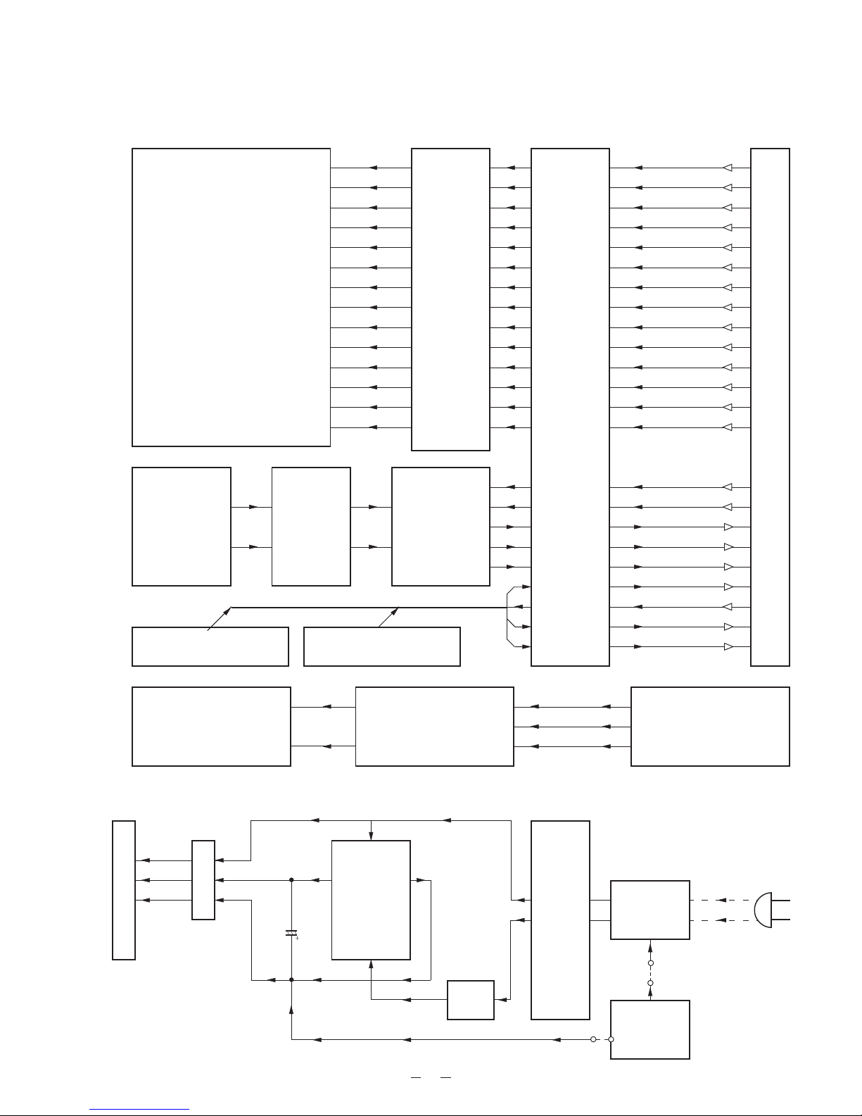
Block Diagrams................................................................................................................................ 6
Tuner.......................................................................................................................................... 6
AMP ........................................................................................................................................... 7
CD.............................................................................................................................................. 8
MD Unit ...................................................................................................................................... 9
Display Unit .............................................................................................................................. 10
PS Unit ..................................................................................................................................... 10
CD MD Test ................................................................................................................................... 11
CD Adjustments ............................................................................................................................. 12
CD Troubleshooting ....................................................................................................................... 15
Operation Troubleshooting............................................................................................................. 25
PCB Views .................................................................................................................................... 26
Tuner PCB Top ........................................................................................................................ 26
AMP PCB Top.......................................................................................................................... 27
Display PCB Top/Bottom................................................................................................................ 28
MD PCB Top/Bottom...................................................................................................................... 29
CD PCB Top/Bottom ...................................................................................................................... 31
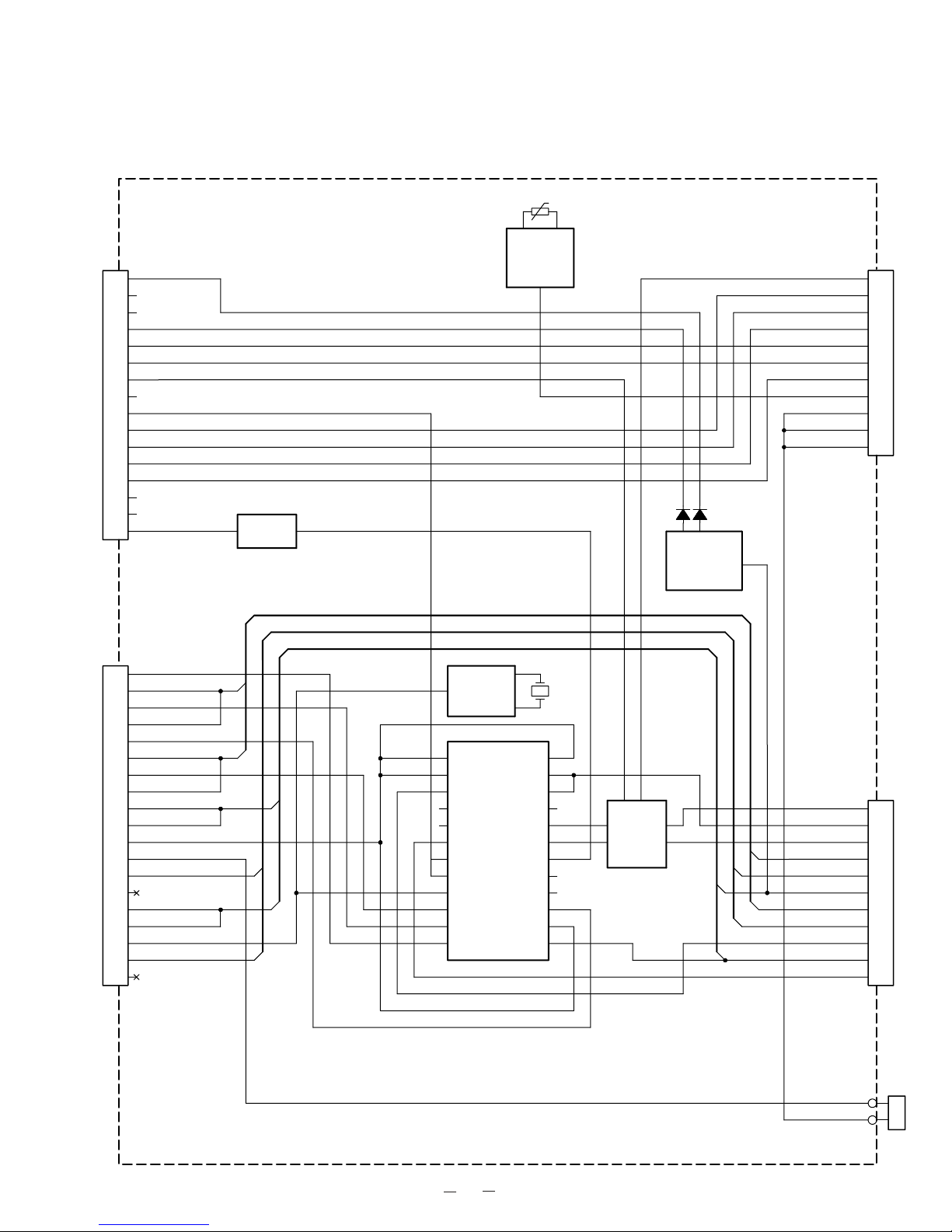
Wiring Diagram .............................................................................................................................. 33
IC Lead Identification and Internal Diagrams ................................................................................. 34
Schematic Diagrams ...................................................................................................................... 46
Tuner........................................................................................................................................ 46
AMP, PS................................................................................................................................... 47
MD ........................................................................................................................................... 48
CD............................................................................................................................................ 49
Front......................................................................................................................................... 50
Parts List ........................................................................................................................................ 51
Exploded Views.............................................................................................................................. 55
IMPORTANT:
DEMONSTRATION
CONDENSATION
When the power cord is plugged into an AC household outlet or the unit is loaded with the
batteries, Demonstration Mode starts. To cancel the Demonstration mode, press the
POWER button or hold the BBS button pressed for more than 3 seconds.
When the unit is moved to a location where the temperature is around 0 degrees C to a
warm location, the unit may not function properly. It is due to condensation generated
inside the unit. Leave the unit for about one hour to let it dry before normal operation.
Page 3

SPECIFICATIONS
MD SECTION
System: MiniDisc digital audio system
Laser: Semiconductor laser
Error correction: Advanced cross interleave read Solomon code (ACIRC)
Channel: 2 channels
Frequency response: 20 to 20,000Hz +/-3dB
Wow and flutter: Less than measurement limit
Recording system: Magnetic field modulation overwrite method
Coding: Adaptive Transform Acoustic Coding (ATRAC)
CD SECTION
System: Compact disc digital audio system
Laser: Semiconductor laser
Channel: 2 channels
Frequency response: 20 to 20,000Hz !3dB
Wow and flutter: Less than measurement limit
TUNER SECTION
Tuning range: FM: 88 to 108MHz
AM: 530 to 1710kHz for Model-B
: 530 to 1600kHz for Model-C
Antenna: FM: Telescopic antenna
AM: Loop antenna (supplied)
GENERAL SECTION
Dimensions: 360 (W) x 158 (H) x 244 (D)
Weight: 4.0kg (without batteries)
Power source: AC 120V, 60Hz for Model-B
: AC 230V, 50Hz for Model-C
DC 9V, 6 x “D” size (R20P)
Power consumption: 21W
Output power: 2.5 (W) + 2.5 (W)
Design and specifications are subject to change without prior notice.
1
Page 4
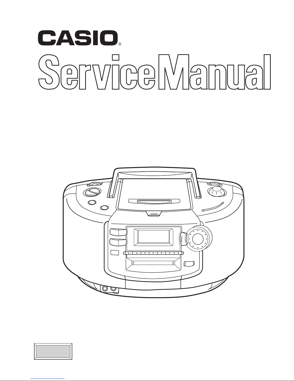
DISASSEMBLY INSTRUCTIONS
1. Remove the battery cover and batteries.
2. Remove ten screws A holding case B unit.
Case B Unit
Battery Cover
Figure 1
3. Open the CD door, remove four screws B holding the case kit.
CD Door
Top Panel Kit
CaseKit
Figure 2
2
Page 5
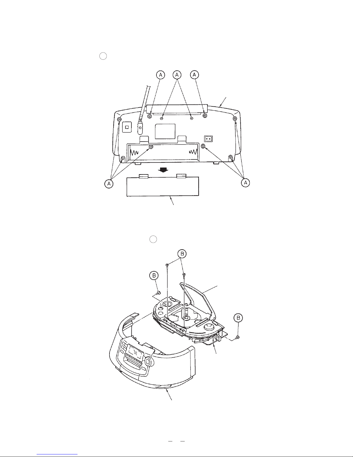
4. Pull out the function knob and tuning knob.
5. Remove four screws C holding the tuner unit.
6. Remove four screws D holding the AMP unit.
7. Remove nine screws E holding the CD unit.
8. Remove three screws F holding the CD mechanism set.
Function Knob
Tuning Knob
Top Case Assembly
9. Pull out the jog knob.
10. Remove six screws G holding the MD assembly.
11. Remove seven screws H holding the display unit.
12. Remove screw I holding the LED PCB.
AMP Unit
Figure 3
CD
Mechanism
Set
CD Unit
Tuner Unit
Model-C only
LED
PCB
Jog Knob
Figure 4
MD Assembly
I
Case Assembly
3
Page 6
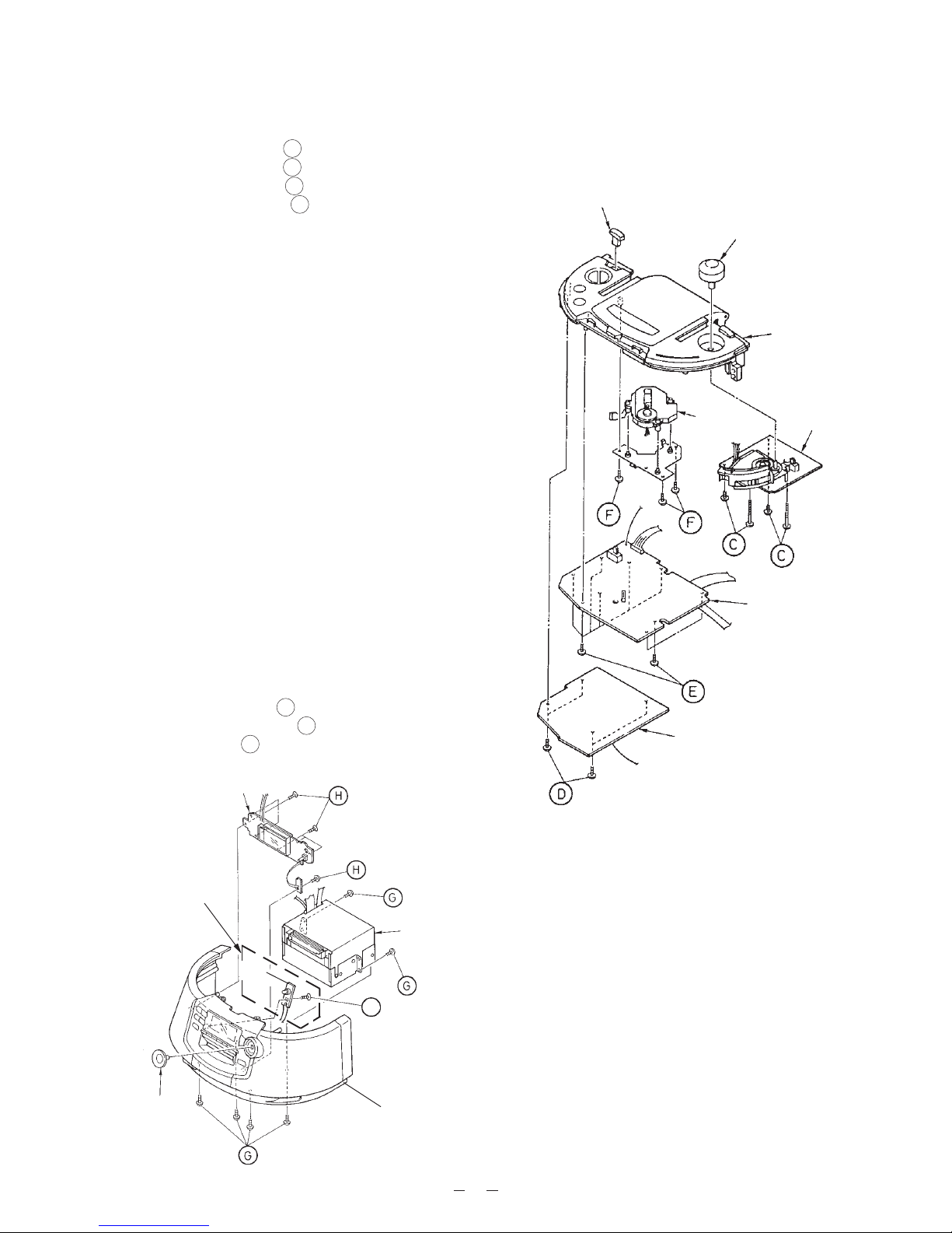
REASSEMBLY OF TUNING POINTER
1. Turn the varicon unclockwise stop position.
2. Set the pointer ; mark position. (refer figure 6)
3. Set the varicon gear of figure 6 position.
4. Insert the tuner gear, fixed the screws L ( tuner collar and tuner plate) and K. (refer figure 5)
K
Varicon Gear
Pointer
Tuner Gear
Varicon
Tuner Chassis
L
Figure 5
Pointer
Mark
Varicon Gear
Tuner Chassis
Tuner Gear
Figure 6
4
Page 7
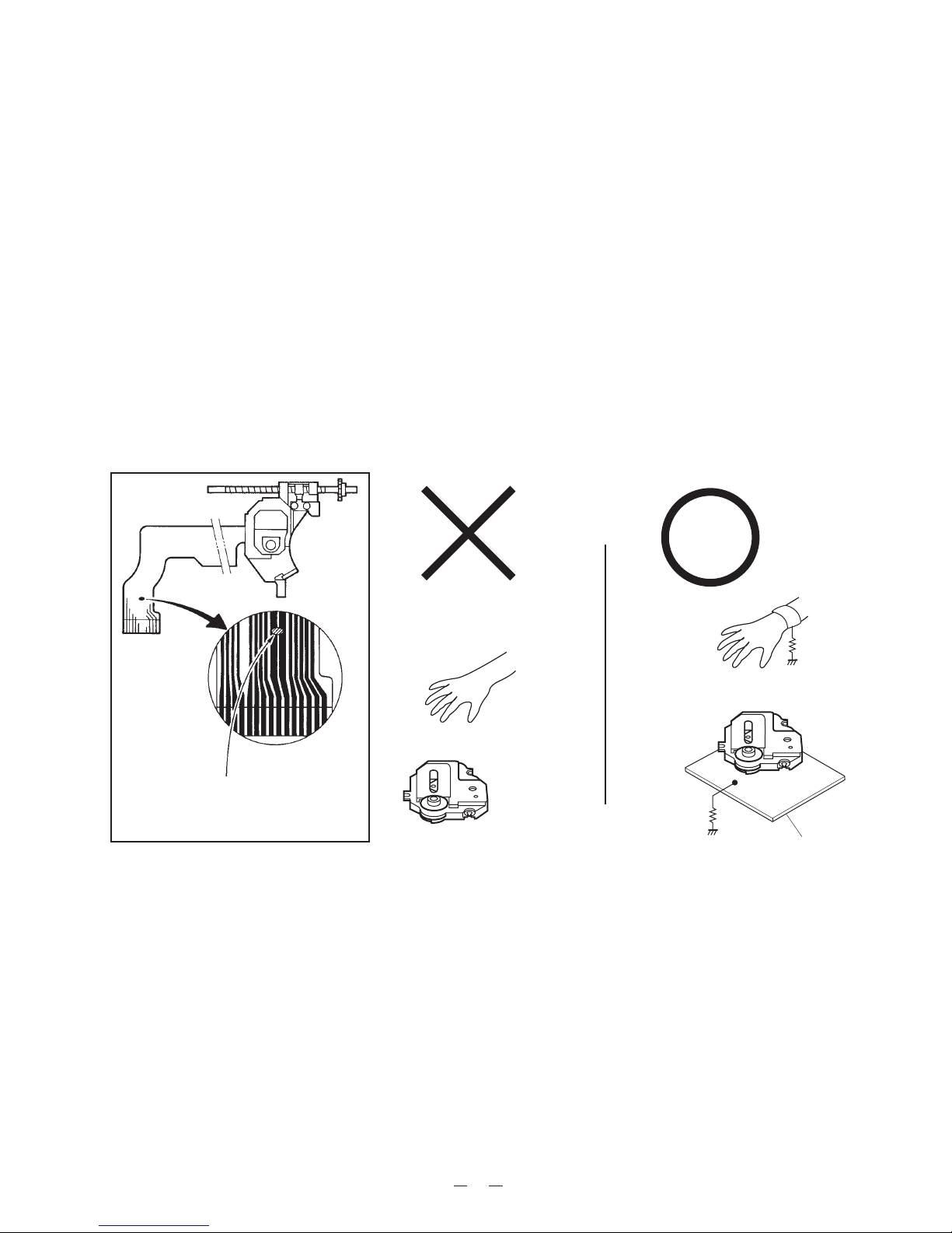
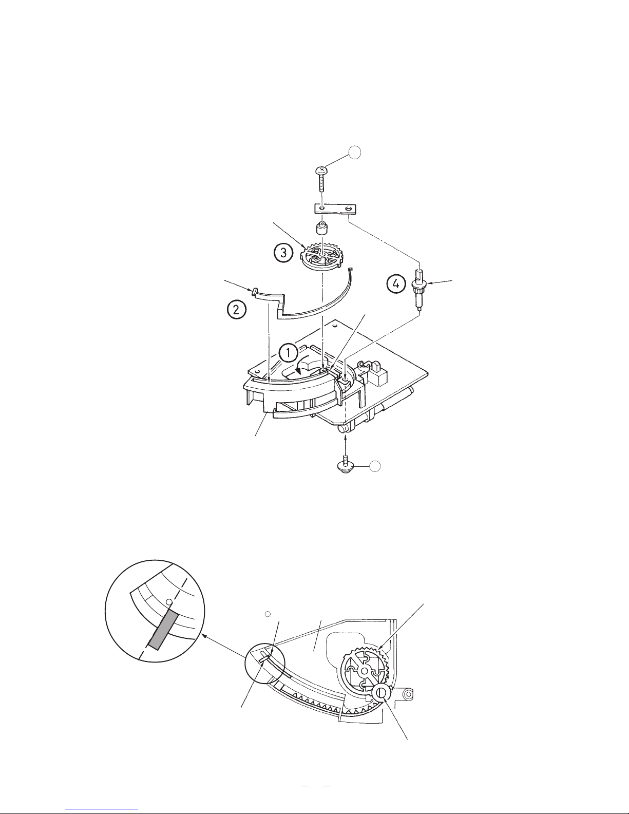
CD PICKUP REPLACEMENT
Precautions
To prevent damage caused by static electricity, the following procedures for grounding is required when opening
or repairing the unit.
1. Grounding for the human body
Be sure to put on a wrist-strap for grounding (with impedance lower than 106 Ω) whose other end is grounded.
The strap works to drain away the static electricity build-up on the human body.
2. Grounding for the work table
Be sure to lay on the table a conductive sheet (with impedance lower than 106 Ω) such as a sheet of copper
which is grounded.
3. As static electricity build-up on clothes is not drainded away, be careful not to let your clothes touch the unit.
4. The short-pad on the pick-up PCB of a spare part is short-circuited for protection during shipment. To open
the short circuit, remove the soldering quickly with a soldering iron whose insulation resistance is larger than
10MΩ after connection to a suitable APC circuit.
Short-pad on pickup PCB
[Note] After the wire connector is
connected, desolder( short-pad).
Pickup
1. Wrist-Strap
for grounding
1MΩ
1MΩ
2. Conductive Sheet
5
Page 8
Tuner
BLOCK DIAGRAMS
Loop Antenna
L2 L5
AM
RF In
FM
RF Out
To Amplifier Block
SW1
AM
BAND SW
FM-MONO
L4
FM
VCC1
22 21 20 19 18 17 16 15 14 1324 23
OSC
FM
OSC
OSC
AM
AF
AM
L3
AM
OSC
AM
DED
DET
Out
MPX In
PRE
FM
AF
AM/FM
SW
FMStereo
LPF1 LPF2
VCO
F.F
GND VCC R ch L ch
VCO
HYS
31 2 4
D3
Decode
SW
FM
RF
FM
MIX
1 2 3 4 5 76 8 9 10 11 12
Rod
Antenna
FM
RF In
GND1
L7
FM Signal
AM Signal
FM MIX AM MIX
AM
MIX
AGC
L8
AGC
AM
IF
VCC2
CF1
Level
DET
AM IFInFM IF
CF2
FM
IF
In
TUN
LED
GND2 QUAD
6
ST
LED
FM
DET
L9
Page 9
AMP
Speaker
L ch
Speaker
R ch
J400
PSCONT
VCC 9V
CN403
STB
DATACKBBS
CN404
AFMUTE
Power
Circuit
Amplifier
Mute
Circuit
Circuit
Volume
Electron
BBS
Circuit
IC402
Q204
Q304
Q202
Q302
IC401
Q403
Q404
Q405
(DC 7V)
Q402/D400
Q400/Q401
Lipple Filter Circuit
IC404
Circuit
MD Power Supply
Circuit
Equalizing
CN402
MD Play L ch
MD Play R ch
Q200/Q300
Q201/Q301
Q203/Q303
CN403
CD Play L ch
CD Play R ch
CN400
Tuner In L ch
Tuner In R ch
CN401
Line In L ch
Line In R ch
7
IC403
Record Amplifier
CN402
MD Record L ch
MD Record R ch
V-BAT. Carcuit
D417/C421/R430
CN402
MD V-BAT.
CN402
MD 5.5V (DC)
Q452/D450
EL Drive Power Supply Circuit
ELCONT
EL PS 3.5V
Page 10
CD
PS Unit
MD Unit
Display Unit
Amp Unit
Q711
Remote
Power
Control
SW706
Door SW
Q901,902
Mute
Circuit
Q702
Laser
Power
Driver
IC709
MD
Bus
Level
Shifter
Q713
Door SW
Driver
IC707
Analog
Filter
IC705
+5V
Power
Driver
+5V
IC705
System
Reset
Circuit
IC704
Micro
Processor
IC702
Digital
Signal
Processior
AC9V
Q709,710
Low Battey
Detect
Circuit
X703
16MHz
X702
32.769KHz
+5V
X701
16.93MHz
+9V
Q707,903
+9V
Power
Driver
Q708
Power
Control
Driver
IC708
CD +5V
Power
Driver
GND
VCC9V
+5V
Function
+9V
+9V
SW701
SW
+9V
Q704,705
CD +9V
Power
Driver
+9V
Q701
Laser
Driver
CD
Mechanism
Q702,703
Anti
Traverse
Circuit
Objective
8
Lens
IC701
Servo
Signal
Processor
Laser
Coupler
M
Disc
Motor
IC703
Motor
Driver
Motor
M
Sled
Reset
Switch
Page 11
MD Unit
TH501
2
1
SYS_+3.3V
1
2
3
VBAT
4
SYSTEM-RST
5
POWER-DOWN
6
7
8
DA-RST
9
RXD
10
TXD
11
12
13
14
15
16
CN501
16P(FFC)
TO BD BOAD
(CN103)
TO MD BOAD
(CN102)
CN502
19P(FFC)
ADDT
1
M-GND
2
BCK
3
4
5
6
7
8
9
10
11
12
13
14
15
16
17
18
19
AMUTE
RTS
CTS
EMPHASIS
M-GND
DADT
M+5V
LRCK
M+5V
GND
GND
3.3V-OUT
D-IN
H+5V
D OUT
+5V
+5V
512FS
H-GND
256FS
INVERT
Q501
1
2
3
4
5
6
7
8
9
10
11
12
OSC
IC502
TC7WU04
IC503
VCC1
VCC1
VINR
VREF1
VREF2
VINL
1PDAD
1PDDA
SYSCK
LRCIN
BCKIN
DOUT
PCM3003
TEMP
DETECTOR
IC505
BA10358
X501
22MHz
24
VCC2
23
AGND1
22
AGND2
21
VCOM
20
VOUTR
19
VOUTL
18
DEM0
17
DEM1
16
ZOBIT
15
DIN
14
VDD
13
DGND
MUTE
CIRCUIT
Q502
Q503
Q504
D502
S-81340HG
D501
1SS133
POWER
SUPPLY
IC501
TO CD PCB
CN504
MD_MUTE
RXD.
TXD.
RTS.
SYSTEM_RST
P_DOWN
CTS.
TEMPDET
GND_UCOM
TO AMP PCB
CN503
MD_OUT(R)
A_GND
MD_OUT(L)
M+5V.
H+5V.
DGND(M)
DGND(H)
A_IN(R)
SYS_GND
A_IN(L)
11
10
9
8
7
6
5
4
3
2
1
1
2
3
4
5
+5
6
7
8
9
10
11
JOIN
WIRE
FROM
D_OUT(CD)
D_GND(CD)
CD PCB
1
2
9
Page 12
Display Unit
MD Out
Switch
SW962
Rotary Encoder
LCD Module
LC950
EN950
CN953
Remocon Photoreceiver
IC951
CN951
Control Switch
Circuit
SW950~SW961
CN952
(DB7)
(DB6)
(DB5)
(DB4)
(DB3)
(DB2)
(DB1)
(DB0)
(E)
(RW)
(RS)
(V0)
(5V)
(GND)
(GND)
(5V)
(KEYIN3)
(KEYIN2)
(KEYIN1)
(REMOTE)
(REMOPOWER)
(JOG1)
(JOG0)
From CD UNIT
EL Panel
EL950
PS Unit
(AC)
(GND)
(+8V)
To CD UNIT
CN101
C105
EL Draive Circuit
Rectification
Circuit
D101~D104
IC951
10
Fuse
F101
(VCC)
(GND)
(EL-CONT)
Power
TRANS.
T101
From AMP UNIT
J101
AC Jack
AC Cable
Battery
9V
Page 13
CD MD TEST
1) Check of CD Mechanical Unit
Item Check Test CD Check Way
Interruption in
a
Information Layer
Black Dot on
b
Read Out Side
c Finger Print
Scratch on Read
d
Out Side
e Eccentricity
Vertical Deviation
f
Sound Skip for
g
Sound Pressure
TCD-726
(A*BEX)
TCD-726
(A*BEX)
TCD-726
(A*BEX)
TCD-721R
(A*BEX)
TCD-712R
(A*BEX)
TCD-732RA
(A*BEX)
TCD-784
(A*BEX)
By using track No.6 (0.5 mm), there shoud not be no noise and no
skip on the playback sound.
By using track No.13 (0.5 mm), there shoud not be no noise and
no skip on the playback sound.
By using track No.18, there shoud not be no noise and no skip on
the playback sound.
By using track No.2 (0.4 mm), there shoud not be no noise and no
skip on the playback sound.
By using the disc (140 ! 5 µm), there shoud not be no noise and
no skip on the playback sound.
By using track No.9 (650 µm), there shoud not be no noise and
no skip on the playback sound.
By using track No.23 (20Hz~2kHz), there shoud be no noise and
no skip on the playback sound at volume Max./ BBS On.
2) Test CD
The following Test CDs are available from A*BEX or parts center of Casio.
Item Part code Part Name Specifications Test Purpose
a~c 1904 5424 Test CD TCD-726 (A*BEX) Defects Test
d 1904 5423 Test CD TCD-721R (A*BEX) Scratch Test
e 1904 5421 Test CD TCD-712R (A*BEX) Eccentric Test
f 1904 5422 Test CD TCD-732RA (A*BEX) Vertical Deviation Test
g 1904 5425 Test CD TCD-784 (A*BEX) Function Test
3) Check of MD Mechanical Unit
* MD Mechanical Unit cannot be adjusted in the field. Only the MD factory can adjust by using special equipment.
a. Playback Test
* Any regular music MD can be used. However the music MD should be supplied by Authorized Music Company, and the
surface of internal disk should be no scratch.
EX) Music MD SRLY-7233 (Sony) can be recommended.
* There should be no any noise on the playback sound for the aging check.
b. Record Test
* Any regular MD can be used. However the regular MD should be supplied by Authorized MD company, and the surface
of internal disk should be no scratch.
EX) Test MD MDW-74 (Sony) can be recommended.
* There should be no any noise on the playback sound after record for the aging check.
4) Test MD
The following Test MDs are available from A*BEX or parts center of Casio. However Test MDs of Sony cannot
be available from Casio.
Item Part code Part Name Specifications Test Purpose
a 1904 5428 Test MD TMD-321W (A*BEX) Scratch Test
b 1904 5429 Test MD TMD-325W (A*BEX) Defect Test
c 1904 5433 Test MD TMD-381 (A*BEX) Function Test
11
Page 14
CD ADJUSTMENTS
Pre-Adjustment Procedures
* Remove the bottom chassis assembly. (Refer pages 3, 4)
* Use the plastic screwdriver.
Equipment Required
* Oscilloscope
* Screwdriver (Plastic type)
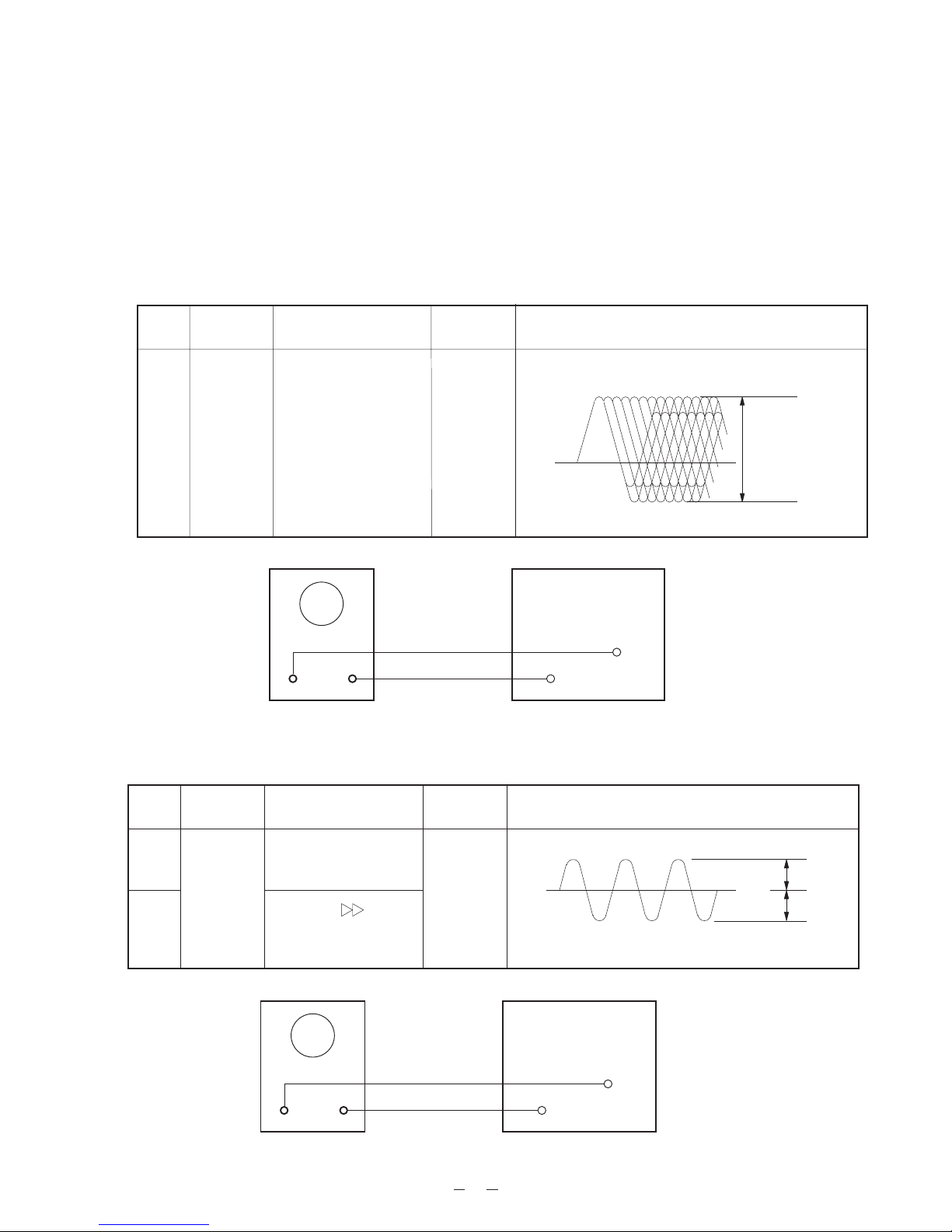
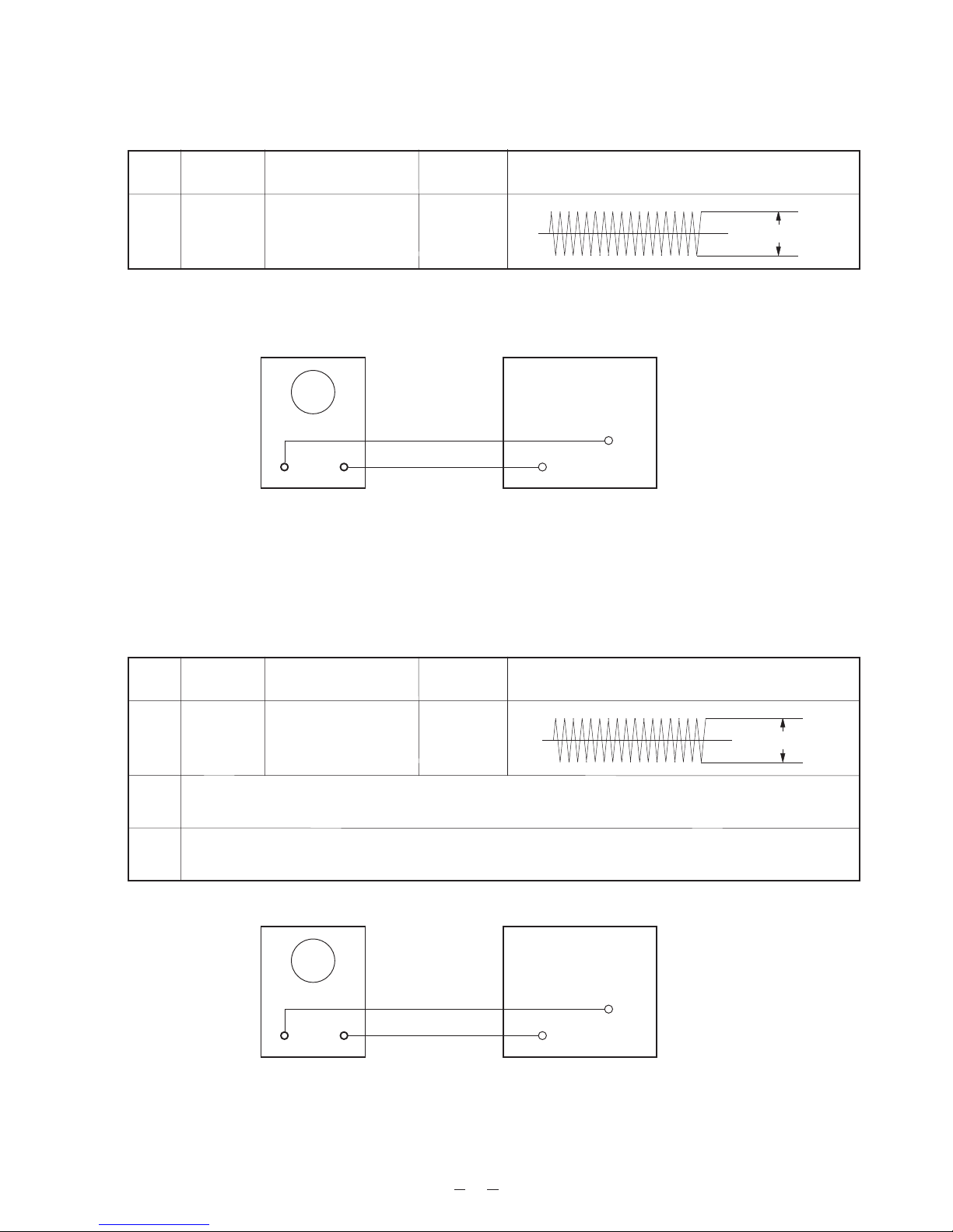
Focus Sarvo Offset Adjustment (Figures 7 and 11)
Step Connect Setting Adjust Result
1
Figure 7
Play the regular disc.See
VR702
Adjust VR701 for the amplitude of the waveform
at maximum.
0V
Measuring on oscilloscope.
Oscilloscope
CD PCB
TP709
GND
TP710
Figure 7
Focus Servo E-F Balance Adjustment (Figures 8 and 11)
Step Connect Setting Adjust Result
>1.0V p-p
Play the regular disc.1
See
Figure 8
2
Keep the button
depressed.
Oscilloscope CD PCB
VR702
GND
Figure 8
12
E-F balance signal
TP706
TP710
0V
(Vref)
A=B
A
B
Page 15
Focus Servo Gain Adjustment (Figures 9 and 11)
Step Connect Setting Adjust Result
1
See
VR704Play the regular disc.
Figure 9
Oscilloscope CD PCB
GND
Figure 9
Tracking Servo Adjustment (Figures 10 and 11)
0V 250 mV p-p
TP750
TP710
Step Connect Setting Adjust Result
1
Figure 10
VR703Play the regular disc.See
0V 100 mV p-p
2 Swap the regular disc for the test disc A*BEX TCD-726 and play it at the black dod of 600 µm.
Confirm that there is no skipping.
3
If there is any skipping, adjust VR 703 to reduce the tracking servo gain until no skipping occurs.
Oscilloscope
GND
CD PCB
TP751
TP710
Figure 10
13
Page 16
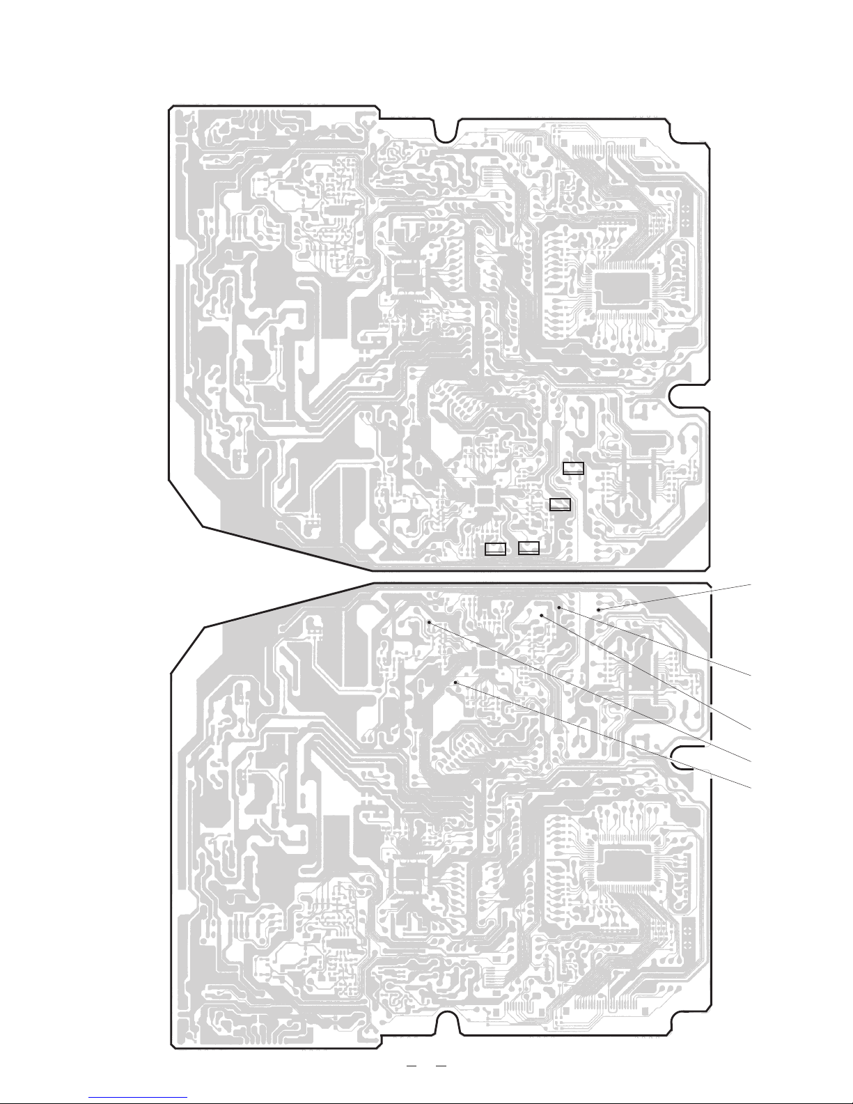
CD Adjustment Points
Top View
VR701
Bottom View
VR704
VR702
VR703
TP750
TP710
TP706
TP751
TP709
Figure 11
14
Page 17
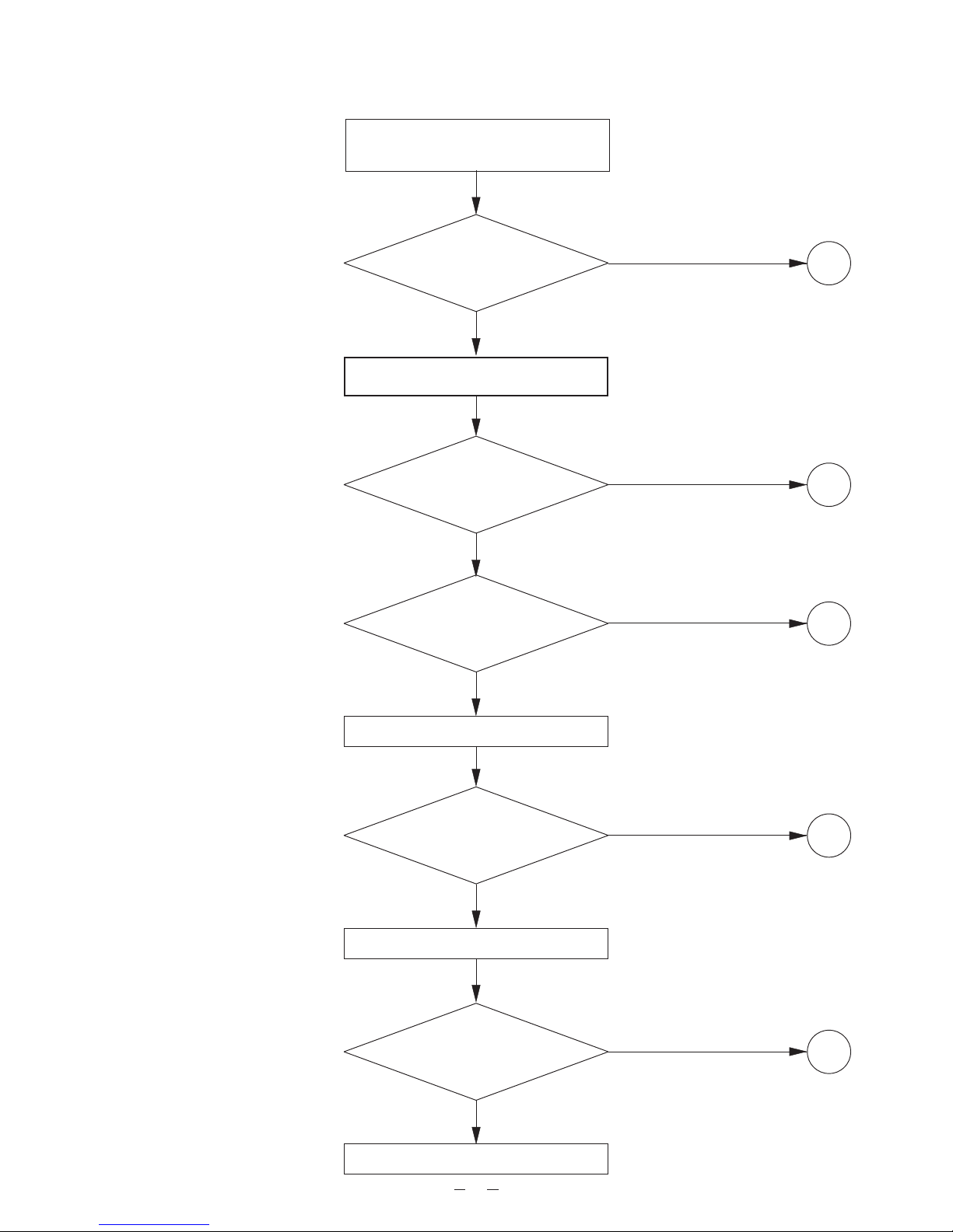
CD TROUBLESHOOTING
Open CD door and set function switch
for CD position.
Is “CD OPEN”
display on LCD ?
Yes
Load a disc close CD door.
Is “CD CLOSE”
display on LCD ?
Yes
Are total track
number displayed?
Yes
No
1
No
2
No
3
Press PLAY/PAUSE key.
Is the audio signal
present at the output
terminals ?
Yes
Press SEARCH key.
Can a selected
track number be searched
smoothly ?
Yes
OK
No
4
L ch: CN709-9 pin
R ch: CN709-7 pin
No
5
15
Page 18
1. “CD OPEN” is not displayed.
1
Is +5 V lines pin 72
of IC704 normal ?
Yes
Is the waveform
at pin 30 of IC704 like that
shown in Fig. 12 ?
Yes
Does 16 MHz
clock pulse appear at
pin 31of IC704 ?
Yes
* Check IC704.
* Check circuit around IC704.
* Check soldering CN705 and FFC.
No
No
No
* Check IC705.
* Check circuit around IC705.
* Check Q713.
* Check circuit around IC706.
* Check X703.
* Check circuit around X703.
100 mS
5 V
Power on
Figure 12
16
Page 19

2. “CD CLOSE” is not displayed.
2
Is the waveform
at pin 43 of IC704 like that
shown in Fig. 13 ?
Yes
Is the waveform
at base of Q713 like that
shown in Fig. 14 ?
Yes
Does +5 V output
appear at pin 1 of
IC708 ?
Yes
Does +9 V
appear at pin 3 of
IC704 ?
No
No
No
No
* Check IC704.
* Check circuit around IC704.
* Check Q713.
* Check SW706.
* Check IC708.
* Check circuit around IC708.
Yes
Does +9 V
appear at emitter
of Q704 ?
Yes
* Check Q707, Q708 and Q903.
* Check circuit around Q707, Q708
and Q903.
5 V
Door close
Figure 13
Figure 14
No
5 V
Door close
* Check Q704 and Q706.
* Check circuit around Q704 and Q706.
17
Page 20

3. Total track number is not displayed.
3
Check how much times it takes until “NO DISC” is
displayed after CD door has closed.
About
6 sec
A
About
10 sec
B
About
15 sec
C
18
Page 21

3-A
A
Does the LASER emit ?
Yes
Dose the lens move
up and down ?
Yes
Load a disc and close CD door.
Then check the following.
Note: Open the CD door and check the radiation
!
power with an optical power meter or by watching
the radiaation through the lens of the pickup unit at
a minimum distance of 30cm from the pickup.
!
No
A1
!
No
A2
E=more than 1V
Figure 15
Figure 16
Figure 17
E
5V
>2V
>0.3V
Is the waveform
at pin 31 (RFO) of IC701 like
that shown in Fig. 15 ?
Yes
Is the waveform
at pin 25 (FOK) of IC701 like
that shown in Fig. 16 ?
Yes
Is the waveform
at pin 1 (FE) of IC701 like
that shown in Fig. 17 ?
Yes
Is the waveform
at pin 2 (FEI) of IC701 like
that shown in Fig. 18 ?
* Check CN701.
No
* Check soldering IC701.
* Check IC701.
* Check pickup.
* Check pins 25, 26 and 27 of IC701.
No
* Check IC701.
No
* Check IC701.
* Check pins 1 and 2 of IC701.
* VR704 adjustment is no good.
No
Readjust VR704.
(Refer to CD Adjustments)
Figure 18
* Check circuit around IC701.
Yes
19
Page 22

3-A1
A1
3-A2
* Check circuit around Q701.
* Check CN701.
* Check Q701.
* Check pickup.
A2
Dose +9 V
appear at pins 19 of
IC703 ?
Does <3 V
appear at pin 33 (LD)
of IC701 ?
Yes
No
No
* Check IC701.
* Check circuit around IC703.
Yes
Is waveform at
pin 16 of IC703 like that
shown in Fig. 19 ?
Yes
* Check CN701.
* Check pickup.
No
Figure 19
Is waveforn at
pin 6 (FEO) of IC701 like
that shown in Fig.20 ?
Yes
* Check circuit around
IC701.
* Check IC703.
1.10V
No
* Check circuit around
and soldering IC703.
* Check IC701 and IC702.
750mV
Figure 20
20
Page 23

3-B
B
Does
disc motor rotate ?
Yes
No
Does CD mechanism
operateing normary ?
Yes
Is waveform at
pin 13 of IC703 llike that
shown in Fig. 21 ?
Yes
No
No
* Check CD mechanism
* Check CD turn table unit.
* Check CN702 and CN703.
* Check disc motor.
* Check soldering IC702.
* Check IC702.
Is waveform at
pin 11 of IC703 like that
shown in Fig. 22 ?
Yes
* Check CN703.
Figure 21
21
No
* Check soldering IC701.
* Check IC701.
2.5V
Figure 22
Page 24

3-C
C
Is waveform at
pin 42 (TEO) of IC701 like that
shown in Fig. 23 ?
Yes
Is waveform at
pin 44 (TE1) of IC701 like that
shown in Fig. 24 ?
Yes
Is waveform at
pin 13 (TAO) of IC701 like that
shown in Fig. 25 ?
Yes
No
No
No
Is pin 3 (DEFECT)
of IC701 high ?
* Check CN701.
* Check IC701.
* Check circuit around TE-Amp lines.
* VR703 adjustment is no good.
Readjust VR703.
(Refer to CD Adjustments)
No
* Check IC701.
Is waveform at
pin 18 of IC703 like that
shown in Fig. 26 ?
Yes
* VR704 adjustment is no good.
Readjust VR704.
(Refer to CD Adjustments)
* Check pickup.
100mV
Figure 23 Figure 24
No
* Check circuit around IC703.* Check CN701.
50mV
Yes
* Check circuit around IC701.
* Check IC701.
200mV
Figure 25 Figure 26
0.4V
22
Page 25

4. No audio signal to output terminals.
4
Does audio signal
appear at pins 1 and 7
of IC707 ?
No
Does 4.23 MHz
appear at pin 11 (CLOK)
of IC702 ?
Yes
Does 88.2 kHz
appear at pin 42 (LRCK)
of IC702 ?
Yes
Does digital signal
appear at pin 9 (DATA)
of IC702 ?
Yes
* Check Q901 and Q902.
* Check circuit around Q901 and Q902.
No
No
No
Yes
* Check IC707.
* Check circuit around IC707.
* Check circuit around and soldering
IC702.
* Check IC702.
23
Page 26

5. Selected track number cannot be searched.
5
Press the” “ or “ “ key.
0
Figure 27
Figure 28
0
pin 42 (TEO) of IC701 like that
pin 42 (TEO) of IC701 like that
* Check IC701.
Is waveform at
shown in Fig. 27 ?
No
Is waveform at
shown in Fig. 28 ?
No
Yes
Yes
* VR702 adjustment is no good.
Readjust VR702.
(Refer to CD Adjustments)
* Check CD mechanism and disc
motor.
* Check pickup.
24
Page 27

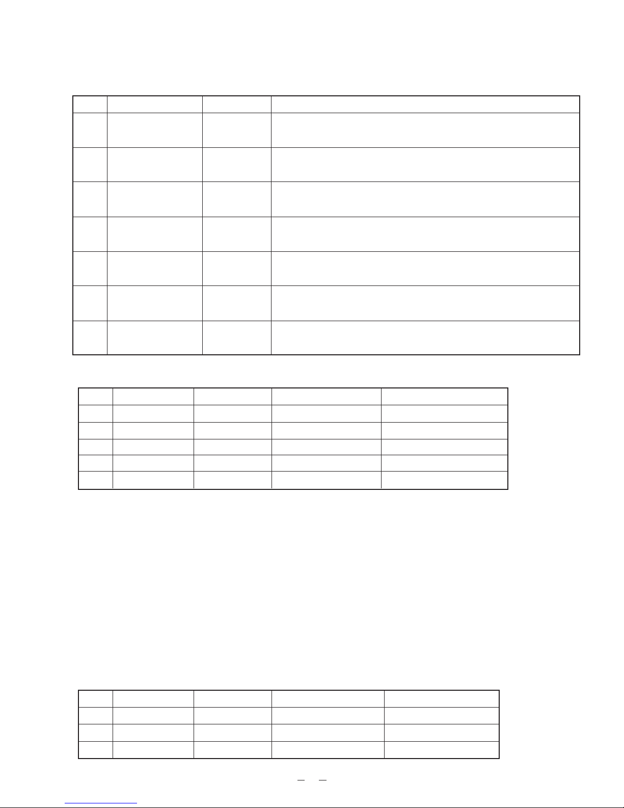
OPERATION TROUBLESHOOTING
Symptom
No operation after power cord is
plugged into an AC household outlet.
Only LCD display is scrolling.
The unit functions are not properly
when the unit is moved to a location
where the temperature is cold to warm.
Sound skip occurs during CD play.
Recording is not possible.
Even if an MD is loaded, “NO DISC” or
“ERROR” appears.
Playback sound is interrupted.
Remote controller is not possible.
The unit under DEMONSTRATION mode.
Due to dew condensation of inside, the unit cannot
work properly.
The unit is used in a location subject to shock and
vibration.
The condition of the disc is bad. Dirt, scratches or warp
exists.
MD is in a state of prevention of accidental erasing.
A pre-recorded MD (MD only for play) is used.
MD is in a state of TOC FULL.
The disc is scratched.
MD is used in an unstable location subject to vibration.
Condensation has occurred.
An MD or CD is not loaded in the unit.
Cause Countermeasure
Press the power button or hold the BBS
button pressed for more than 3 seconds.
Leave the unit for about one hour to let it
dry before normal operation.
Change the installation location.
Wipe the CD to remove the dirt. If the
CD is scratched or warped, it cannot be
used.
Move the accidental erasing tab to the
recordable side.
Replace it with a recordable MD.
Replace it with a new recordable MD.
Replace it with a new MD.
Move the unit to a level, stable location.
Leave the unit for about one hour to let it
dry and then operate it.
Insert an MD or CD is into the unit.
Error Message when operating MD
When such a display appears Cause Countermeasure
NO DISK
DISK ERR
?DISK
DISK FULL
BLANK MD
00:00
PLAYBACK MD
NAME FULL
MECHA ERR#
# means figures and symbols.
PROTECTED
TOC FULL#
# means figures and symbols.
TEMP OVER
Can’t EDIT
*An MD is not loaded.
*Data on the MD cannot be read.
*The disc is scratched.
*TOC is not written on the MD or data is abnormal.
*TOC information cannot be read.
*An MD not conforming to standards is used.
*Data other than audible data has been recorded.
*TOC information is not made properly due to shocks
or scratches on the disc.
*TOC information recorded on the MD does not
conform to the standards or cannot be read.
*Data is abnormal and an MD not conforming to the
standards is used.
*This indication is displayed when recording is made
immediately after loading an MD. It is due to the
fact that TOC information has not been read.
*There is no blank section on the MD to record on.
*A blank disc is used. (Neither music nor disc name
is written.)
*Music has not been recorded.
*Recording or editing has been made using a pre-
recorded MD (MD only for play).
*The disc name or the track name exceeds the limit
of 100 characters.
*MD does not function properly.
*The MD is in the accidental erasure prevention
state.
*There is no blank section where track numbers and
character information (disk name and track name)
can be written.
*The temperature has been markebly increased
inside the unit.
*Editing is not performed.
*Insert an MD.
*Insert the MD again.
*Insert the MD again.
*Replace the MD with another one.
*Select another track.
*Change the MD.
*Turn off the power and write TOC again. Do not
give the unit a shock while the TOC is written.
*Replace the MD with another one.
*Erase all data on the MD and record again.
*Replace the MD with another one.
*Wait unit TOC information on the MD has finished
being read.
*Replace the MD with another recordable one.
*Use a pre-recorded MD to play.
*Use an MD on which music has been pre-
recorded.
*Replace it with a recordable MD.
*Shorten the disc name or the track name.
*Turn off the power and remove the MD.
*Move the prevention tab the recordable side.
*Replace the MD with another recordable one.
*Turn off the power and do not operate the unit
until the temperature returns to normal.
*Change the position where the music stops and
try to perform editing again.
25
Page 28

Tuner PCB Top
PCB VIEWS
26
Page 29

AMP PCB Top
27
Page 30

Display PCB Top
Display PCB Bottom
28
Page 31

MD PCB Top
29
Page 32

MD PCB Bottom
30
Page 33

CD PCB Top
31
Page 34

CD PCB Bottom
32
Page 35

33
LCD Panel
Shield Plate
Speaker R ch Speaker L ch
CN954
114
114
1
23
CN952
1
DISPLAY PCB
Heat Sink
1 MD SW PCB
JACK PCB
1
1
7
4
TUNER PCB
1
4
Telescopic Antenna
Battery 1.5V x 6
1 2
BATTERY PCB
1
3
41
1
3
CN405
CN406
CN407
144
1
1
7
1
7
CN401
CN404
AMP PCB
2 1
CN101
13
PS PCB
Model-C
Only
1 2
4 1
CN400
1
9
1
11
CN402
CN403
LED
PCB
1
15
Red
Black
1 2
2 1
Pickup
Preset Switch
Sled MotorDisc MotorPickup
CD MECHANISM
CN704
CN702
CN703
CN701
1 2
1 2
15
1
1 2
3
1
CN710
19
CN709
White
Shield
7
1
CN707
CN706
1 11
1 23
CN705
111
11
1
13
1
1
19
CN501
CN502
CN503
CN504
Shield
White
Shield
White
White
Shield
CD PCB
MD PCB
16 1
19 1
CN103 CN102
MD MECHANISM
WIRING DIAGRAM
Page 36

IC3: TA8167N
24
IC LEAD IDENTIFICATION AND INTERNAL DIAGRAMS
13
FM
12
AM
AM
DET
AM
IF
DET
Out
MPX In LPF1 LPF2 VCO L ch Out R ch Out
PRE
FM
AF
AM/FM
AM IF In
SW
Level
DET
FM IF In
FM
IF
GND2 TUN LED
VCO
F.F
TUN
LED
VCC1 FM OSC AM OSC
22 21 20 19 18 17 16 15 14 13
FM
MIX
FM
OSC
AM
MIX
OSC
AM
AF
AGC
1
AM
RF In
RF Out
24 23
FM
RF
1 2 3 4 5 76 8 9 10 11 12
FM RF In GND1 FM MIX AM MIX AGC VCC2
IC401: TC9260P
16 9
Decode
HYS
ST
LED
ST LED QUAD
SW
FM
DET
Out
LD1
LD2
CS
CK
8
2
3
In
4
5
6
7
8
1
L-ch
Volume
A-GND
V
SS
L-ch
Latch
Data Decoder, STB Generator
Shift Register (13 bit)
34
V
DD
161
R-ch
Latch
15
14
13
12
11
10
9
R-ch
Volume
Out
In
LD1
LD2
A-GND
STB
DATA
Page 37

IC402: TA8227P
12
16
Vcc1
Vcc2
7
B.S. 1 Out 1 Power GND
3 4
2
12
Ch 1
1
6
In 1 NF 1
30 kΩ
45Ω
5
Bias Circuit
Thermal
Shut Down
Protection
Circuit
9
Ripple
OUt 2
11 10
30 kΩ
Ch 2
8
7
In 2 NF 2
45Ω
B.S. 2
Pre GND
(F In)
IC403: BA15218N
1
8
1 2
1 2 3 4 5 6 7 8
Out 1 -In 1 +In 1 GND +In 2 -In 2 Out 2 V
35
CC
Page 38

IC404: PQ15RW11
1 2 3 4
IC501: S-81340HG-KJ-T1
V
1 2 3
IN
Vin
1
IC
3
GND
3
Vref
2
Vo
Vadj
4
*Parasitic
Diode
IC502: TC7WU04FU-TE12L
85
14
2
GND
VCC Out 1 In 2 Out 3
8 7
6
5
V
1
OUT
1 2
In 1 Out 2 In 3 GND
3 4
36
Page 39

IC503: PCM3003E-T1
24
1
VINL
VREF1
VCOM
VREF2
VINR
21
13
12
Analog
6
4
5
3
Front-end
Circuit
Reference
Analog
Front-end
Circuit
(+)
(-)
(+)
(-)
Delta-sigma
Modulator
Delta-sigma
Modulator
Decimation
&
Low Cut Filter
ADC
Decimation
&
Low Cut Filter
Serial
Interface
10
11
15
12
LRCIN
BCKIN
DIN
DOUT
VOUTL
VOUTR
Analog
19
20
AGND2 VCC2 AGND1 VCC1 VCC1 DGND VDD SYSCK
Low-pass
Filter
Analog
Low-pass
Filter
Power Supply
22
Multi-level
Delta-sigma
Modulator
Multi-level
Delta-sigma
Modulator
Interpolation
Oversampling
DAC
Interpolation
Oversampling
Filter X8
Filter X8
Clock
91413212324
Mode
Control
Interface
Reset and
Power
Down
66
18
17
7
8
20BIT
DEM0
DEM1
/PDAD
/PDDA
37
Page 40

IC505: BA10358
85
14
CC
8 7 6 5
2
1
1 2 3 4
Out 1 -In 1 +In 1 GND
+In 2-In2Out 2V
38
Page 41

IC701: CXA1782BR
37
36
25
24
FE
BIAS
VEE
TEO
LPFI
TEI
ATSC
TZC
TDFCT
VC
48
1
13
12
PHD2 PHD1 PHD LD RF M RF O RF I CP CB CC1 CC12
FOK
36
APC
RF
Amp.2
RF
Amp.1
FOK
LEVEL
3132333435
30
MIRR
29
28
27
DFC1
37
FZC
TM1
IIL Date Register
Input Shift Register
Adress Decoder
HPF
Comparator
Comparator
TG1
FCS Phase
Compensation
TOG1~3
BAL1~3
LPF
FS1
FS2
Output Decoder
TG1~2
FS1~4
Tracking
Phase
Compensation
TM1~7
TM6
TM5
TM4
TM3
TM7
TG2
F
E
E
FIV Amp.
38
EIV Amp.
39
40
41
BAL1 BAL2 BAL3
42
TOG1
43
44
45
46
47
48
TOG2
TOG3
Window Comparator
ATSC
EF Amp.
EF Amp.
Defect
TTL
IIL
Comparator
TZC
Comparator
DFCT
FS4
26
PS1~4
I SET
25
TM 2
F Set
IIL
TTL
IIL
TTL
VCC
ISET
SL O
SL M
SL P
TA O
XLT
CLK
24
23
22
21
20
19
18
17
16
15
14
13
SENS
C
OUT
XRST
DATA
9
1 2 3 465 7 8
10 11 12
FEO FEI FDFCT FGD FLB FEO FEM SRCH TGU TG2 FSET TAM
39
Page 42

IC702: CXD2508AR
61
60
41
40
EMPHI
LRCKI
PCMDI
BCKI
MUTE
BCK
PCMD
LRCK
WDCK
C2PO
RFCK
MNTO
MNT1
MNT3
WFCK
EMPH
GFS
XUGF
GTOP
41
43
56
55
54
62
60
49
47
46
61
45
44
42
40
39
52
50
20
EFM
21
D/A
Interface
XTAI
XTAO
71 72 63
Digital Filter
1 bit DAC
Digital
Out
16K RAM
SUB Code
Processor
+
ZEROL
64
ZEROR
Digital
CPU
Interface
CLV
67
68
76
75
59
53
25
24
23
22
3
2
1
80
79
20
16
9
8
7
5
NLPWM
LPWM
RPWM
NRPWM
DOUT
XROF
LOCK
MDS
MDP
MON
SQCK
SQSO
EXCK
SBSO
SCOR
XLON
SPOA~C
CLOK
XALT
DATA
SENS
80
1
4
Error
Corrector
Demodulator
19
XTSL
Clock
Generator
57
FSTT
58 34
C4M
36 37
RF
Asymmetry
Corrector
38 35
ASYI
ASYO
ASYE
40
BIAS
Digital
PLL
48 27 28
FILO
XPCK
FILI
29
PCO
Sequencer
32 21
CLTV
Servo
Auto
11
FOK
12
SEIN
CNIN
15
14
13
CLKO
XLTO
DATO
Page 43

IC703: BA5941FP
28 15
1
VIN4’ VIN4 VIN3’ VIN3 OP Out OP In(-) OP In(+)
27 26 25 24 23 22 21 20 19 18 17 16 15
28
13.3K
13.3K
10K
10K
13.3K
13.3K
10K
7
10K
1
V
BIAS In VIN1’ VIN1 VIN2’ VIN2 GND GND MUTE VCC VO2(-) VO2(+) VO1(-) VO1(+)
CC
3 4 5 6
2
14
GND NC VCC VO3(-) VO3(+) VO4(-) VO4(+)
Level shift
Level shift
Level shift
Level shift
MUTE
8
9 10
11 12 13 14
41
Page 44

IC704: CXP84648-122Q
P14/INT4
P13/INT3
P12/INT2
P11/INT1
P10/INT0
PE5/TO/ADJ
PE4
PE3/NMI
PE2/RMC
PE1/EC1
PE0/EC0
PB7/SO1
PB6/SI1
PB5/SCK1
PB4/SO0
PB3/SI0
PB2/SCK0
PB1/CSO
PB0/CINT
PA7/AN7
PA6/AN6
PA5/AN5
PA4/AN4
PA3/AN3
AN0~AN7
P
T
PWM0
PWM1
RMC
OS0
SI0
SO0
SCK0
SI1
SO1
SCK1
SI2
SO2
SCK2
EC0
TO
CINT
EC1
SCL0
SCL1
SDA0
SDA1
ADJ
6463626160595857565554535251504948474645444342
V
NC
65
66
67
68
69
70
71
72
DD
73
74
75
76
77
78
79
80
P15/SCK2
P16/S12
P17/SO2
PG0
PG1
PG2
PG3
PG4
PG5
PG6
PG7
PF0/SCL0
PF1/SCL1
PF2/SDA0
1234567891011121314151617181920212223
D
D
X
X
PF6/T
PF3/SDA0
AV
SS
8
A/D Converter
D
X
D
X
UART Receiver
URAT Transmitter
UART Baud Rate
Generator
12 Bit PWM Generator 0
12 Bit PWM Generator 1
Remocon In
Serial
Interface
Unit (Ch0)
Serial
Interface
Unit (Ch1)
Serial Interface Unit
8 Bit Timer/Counter 0
8 Bit Timer 1
16 Bit CAPTURE
Timer/Counter 2
Interface Unit
(Ch2)
2
C BUS
I
AV
FIFO
Buffer
RAM
FIFO
REF
PF7/R
PF5/PWM1
PF4/PWM0
INT1
INT0
NMI
NMI
2
2
2
PD3
PD2
PD1
PD0
INT4
INT3
INT2
Interrupt Controller
PD4
PD5
PD7
PD6
SPC700
CPU Core
40K Bytes
Prescaler/
Time Base
Timer
PC0
ROM
PC1
PC2
PC3
PC6
PC5
PC4
XTAL
EXTAL
TX
TEX
Clock
Generator/
System
Control
RAM
2048 Bytes
32 KHz
Timer/
Counter
PC7
PH0
RST
DD
V
PH1
SS
V
41
40
39
38
37
36
35
34
33
32
31
30
29
28
27
26
25
24
PH2
PA2/AN2
PA1/AN1
PA0/AN0
AV
REF
AV
SS
TEX
TX
V
SS
XTAL
EXTAL
RST
PH7
PH6
PH5
PH4
PH3
8
Port APort BPort CPort DPort EPort FPort G
8
8
8
4
2
7
8
8
Port HPort I
8
PA0~PA7
PB0~PB7
PC0~PC7
PD0~PD7
PE0~PE3
PE4, PE5
PF0~PF6
PF7
PG0~PG7
PH0~PH7
PI0~PI7
42
Page 45

IC705: S-81350HG-KD-T1
1 2 3
*Parasitic
V
IN
3
Diode
Vref
V
1
OUT
2
GND
IC706: RH5VL29CA-T1
1 2 3
V
2
DD
1
OUT
Vref
3
GND
43
Page 46

IC707: BA4510F
8
5
14
IC708: NJM2930F05
CC
+In 2-In2Out 2V
2
1
1 2 3 4
Out 1 -In 1 +In 1 V
5678
EE
3 2 1
3
1
2
Input
Output
Common
44
Page 47

IC709: TC74VHCT08AFT
14 8
17
IC950: REC SPS-444-1
1 2 3
4 5
V
CC
4B 4A 4Y 3B 3A 3Y
14 13 1112 10 89
1 32 4 65 7
RL
AMP
Limiter
Detector
Waveform
Shaper
BPF
+
TRAP
ABLC
GND1A 1B 1Y 2A 2B 2Y
3
V
CC
2
V
OUT
1
GND
4
(GND)
IC951: SM8140AM-ET
14
17
8
ENA
CPO
CP1
CP2
10
11
12
5
(GND)
V
DD
LDR CHV OUT1 OUT2
9 2 1 14 13
8
Enable Circuit
High Voltage
Switching Circuit
Charging Pump
Circuit
Level Shifter
Deviding Circuit
Oscillator for
boosting voltage
Level Shifter
Deviding Circuit
Oscillator for
EL
5 4 7 63
VSS1 OCL1 OCL2 OCE1 OCE2
45
Page 48

Tuner
FM-IFT
AM-IFT
0
10
4
R
CF2
FFE1070MA
C29
100PF(B)
C28
C32
FM-QUAD DET
D1
D2
C10 33PF(SL)
CF1
FFD455MB
0.022
100/16V
R5
4.7K
1SS133
1SS133
L6
L7
L8
C30
0.047(X)
SCHEMATIC DIAGRAMS
CN2
ANT1
AIN
FOT
VC1
FOS
AOS
DET
MPX
LP1
LP2
VCO
L CH
R CH
ROD ANT
C26
0.022(X)
PVC FM-RF
C4 18-27PF
24
23
22
R1 27
21
20
19
C14 10/10V
18
17
16
15
14
13
C23*
C22*
R10 15K
FM-ANT
C11
C12
33/10V
L9
C9
15PF(SL)
22PF(SL)
1
2
3
4
5
6
7
8
9
10
11
12
C27
100PF(B)
IC3
TA8167N
FMI
GD1
FMX
AMX
AGC
VC2
AIF
FIF
GD2
TL
SL
QUD
C25 3300PF(X)
D6
SD115
SL(22PF)
L5
FM-RF
C1 22PF
C15
0.33/50V
C16 3.3/25V
C17*
C21 1000PF(P.S)
R8 12K
R9 15K
C3
CH
R7 1K
SVR1
10K (B)
D3
MTZJ5.1B
C20
0.022(X)
C19
100/16V
C7
0.022(X)
R2
100K
5PF(CH)
C2 18-27PF
CH
L4
FM-OSC
C13
PVC FM-OSC
C8
0.022(X)
1000PF(B)
R3 10
FB1
FBA04VA600
C6
0.022(X)
R6 1M
BAND SW
L1
AM LOOP ANT.
(CH)
(8PF)
R13 56K
FM-S
CN1
PVC AM-ANT
L2
AM ANT
L3
AM OSC
FM-M
SW1
C5
3-12PF
PVC AM-OSC
AM
R11
220
1/2W
1
2
3
4
CN3
C24 3300PF(X)
D5
46
1SS133
C18 1000PF(B)
D4
1SS133
*
Model-B Model-C
C17 0.082 0.01
C22 0.018 0.012
C23 0.018 0.012
Notes:
1. All resistance values are in ohms (k=1000 ohms, M=1000 kohms).
2. All capacitonce values are in uF (P=10 uF).
-6
3. All resistors are 1/4 watt, unless otherwise specified.
Page 49

R341
4.7k
1
2
3
4
5
6
7
CN401
FROM JACK
R340
100k
R339
180k
R239
180k
Q308
2SD1302
OUTRCH
OUTGND
OUTGND
OUTLCH
AGND
LMRCH
Q208
2SD1302
R240
100k
R351
150k
R251
150k
1
2
3
4
CN400
FROM TUNER
LMLCH
TLCH
TRCH
R241
4.7k
R201
560k
R203
2.2k
C203
4.7
50V
R204
5.6k
R205
2.2k
R414
10k
Q410
2SA1015
C204
100p
C205
1800p
R208
27k
R209
18k
C207
0.1
R249
10k
C209
4.7
50V
Q201
2SC1815
R214
2.2k
C206
6800p
R212
560k
C211
4.7
50V
R215
39k
R216
39k
R217
180k
C213
6800p
R222
2.2k
R219
330k
C215
1
50V
C212
0.1
50V
R223
2.2k
R247
8.2k
C230
1500p
R248
330k
R406
100
C216
4.7
50V
C217
4.7
50V
C460
47
10V
D460
1SS133
R460
47k
R425
R424
R224
C219
C222
100
16V
R234
220k
Q206
2SC1815
R235
3.3k
R227
330
C223
1000
10V
C404
470
16V
FR401
47(1/4W)
C221
10
16V
R328
2.2
R228
2.2
C325
0.15
C225
0.15
V
C
C
2
1
O
U
T
1
2
B
S
1
3
P
W
G
N
D
1
3
P
R
E
G
N
D
4
N
F
1
5
I
N
1
6
I
N
2
7
N
F
2
8
R
P
L
9
P
W
G
N
D
1
4
B
S
2
1
0
O
U
T
2
1
1
V
C
C
1
1
2
IC402
TA8227P
Q204
2SD1302
Q304
2SD1302
R225
2.2k
R325
2.2k
C218
C318
C220
120p
C320
120p
C224
4.7
50V
C324
4.7
50V
C331
0.1
C231
0.1
R226
10k
R326
10k
D403
1SS133
D409
7.5B
R426
V
S
S
1
O
U
T
2
I
N
3
L
D
1
4
L
D
2
5
A
G
N
D
6
C
S
7
C
K
8
D
A
T
A
9
S
T
B
1
0
A
G
N
D
1
1
L
D
2
1
2
L
D
1
1
3
I
N
1
4
O
U
T
1
5
V
D
D
1
6
IC401
TC9260
R321
39k
R221
39k
R408
10k
R407
10k
C411
1000
10V
C412
22
16V
D462
1SS133
D461
1SS133
Q202
2SC1815
Q302
2SC1815
R318
12k
R218
12k
Q303
2SC1815
C214
470p
C314
470p
Q203
2SC1815
R220
100
R320
100
R310
82k
R210
82k
R211
27k
R311
27k
C308
1000p
C208
1000p
Q301
2SC1815
R213
820
R313
820
C310
2200p
C210
2200p
C202
1000p
C201
1
50V
C302
1000p
Q300
2SC1815
Q200
2SC1815
R202
2.2k
R302
2.2k
R206
100k
R306
100k
R307
5.6k
R207
5.6k
C301
1
50V
C300
4.7
50V
C200
4.7
50V
T9V
AGND
L405
FERRITE
BEAD
L404
FERRITE
BEAD
R350
270k
R250
270k
O
U
T
1
1
I
N
1
2
+
I
N
1
3
V
E
E
4
+
I
N
2
5
I
N
2
6
O
U
T
2
7
V
C
C
8
IC403
BA15218N
R301
560k
R303
2.2k
C303
4.7
50V
R304
5.6k
R305
2.2k
C304
100p
C305
1800p
R308
27k
R309
18k
C307
0.1
R349
10k
C309
4.7
50V
R314
2.2k
C306
6800p
R312
560k
C413
C311
4.7
50V
R315
39k
R316
39k
R317
180k
C313
6800p
R322
2.2k
R319
330k
C315
1
50V
R411
10k
D415
1SS133
C312
0.1
50V
R323
2.2k
R347
8.2k
C330
1500p
C409
22
16V
R410
220
R348
330k
C410
470
10V
C316
4.7
50V
C317
4.7
50V
C408
0.01
R404
10k
R405
10k
C407
3.3
50V
D408
7.5B
D407
7.5B
C319
R324
D405
RB100A
C322
100
16V
C405
2200
16V
R327
330
C406
100
10V
R335
3.3k
Q306
2SC1815
R334
220k
C420
0.47
50V
R418
2.2M
R417
C323
1000
10V
C321
10
16V
C419
1200p
R329
56k
R229
56k
1
2
3
4
5
6
7
CN404
FROM CD
LMUTE
STB
DATA
FTUNER
C401
0.022
C400
2200
16V
1
2
3
4
5
6
7
8
9
CN403
FROM CD
CK
BBS
AFMUTE
ELCONT
VCC9V
DC9V
GND
C402
0.022
Q402
2SC1815
D400
5.6V
Q400
2SB1655
D401
1SS133
R402
100k
R409
4.7k
D406
JUMPER
R422
100k
Q405
2SC1815
R420
47k
Q406
2SC1815
R419
15k
D414
1SS133
R423
Q403
2SA1015
R421
10K
R416
4.7k
R415
4.7k
C329
1
50V
C414
100
10V
C430
100
10V
C457
1
50V
C229
1
50V
R246
470k
R346
470k
R244
270k
R344
270k
C328
1
50V
C228
1
50V
R245
47k
R345
47k
5V(MOTOR)
R338
220k
R238
220k
1
2
3
4
5
6
7
8
9
10
11
CN402
FROM MD
MDRCH
AGND
MDLCH
R242
1k
R342
1k
R343
R243
C403
1
50V
R401
120k
D404
3.9B
R400
1k
12
CN102
CON2
BATTERY
BAT PCB
FMD
CDRCH
CDGND
CDLCH
1
2
J101
AC SOCKET
4
312
T101
PS PCB
12
CN102
CON2
D102
1N5401
D101
1N5401
D103
1N5401
D104
1N5401
C105
3300
25V
C102
0.022
C101
0.022
C103
0.022
C104
0.022
1
2
3
CN101
2
1
L ch
SP
R428
2k
2
2
4
4
3
3
1
1
IC404
PQ15RW11
C416
100
16V
C415
470
16V
R427
1.8K
L400
FERRITE BEAD
D410
1SS133
R429
10k
C418
100
10V
C417
100
10V
L402
FERRITE BEAD
Q452
2SD1302
C452
0.022
R453
390
GND(SYS)
GND(HEAD)
GND(MOTOR)
5V(SYS)
5V(HEAD)
1
2
3
CN405
FROM FRONT
MDRECRCH
MDRECRCH
EL
ELGND
ELCONT
R454
470
C453
47
10V
C451
100
16V
D450
3.9A
C450
100
16V
R450
150
Use the specifed type without fail .
*Parts maker with are of importance in respect to the safty .
1
2
3
4
CN407
FROM JACK
1
2
3
4
CN406
TO SP
1
2
3
4
2
1
R ch
SP
1
2
F101
FUSE Model-B: T2.5A/250V, Model-C: T2.5A/250V
AMP PCB
AMP, PS
Notes:
1. All resistance values are in ohms (k=1000 ohms, M=1000 kohms).
2. All capacitonce values are in uF (P=10 uF).
3. All resistors are 1/6 watt, unless otherwise specified.
-6
47
Page 50

MD OUT(R)
L522
10uH
R521
47k
L507
JP
SYS +3.3V
LEDO
1
2
3
4
5
6
7
8
9
10
11
12
13
14
15
16
CN501
16P(FFC)
TO MD BOAD
(CN103)
C514
TP41
TP42
L509
JP
VCC1
1
VCC1
2
VINR
3
VREF1
4
VREF2
5
VINL
6
1PDAD
7
1PDDA
8
SYSCK
9
LRCIN
10
BCKIN
11
DOUT
12
DGND
13
VDD
14
DIN
15
ZOBIT
16
DEM1
17
DEM0
18
VOUTL
19
VOUTR
20
VCOM
21
AGND2
22
AGND1
23
VCC2
24
IC503
PCM3003
L506
JP
C519
10u
FB557
0
C527
4.7u
C529
4.7u
C528
0.1
C530
JP581
FBA04HA900
FB556
0
FB555
HS601
R523
D504
1SS133
C505
Q502
DTA114E
D503
1SS133
C548
Q504
DTC114T
L501
JP
L502
JP
MD OUT(L)
A GND
L
1
G
2
L
3
EF502
EMIFIL
L
1
G
2
L
3
EF504
EMIFIL
L
1
G
2
L
3
EF505
EMIFIL
L521
10uH
SYS GND
A IN(R)
DGND(H)
DGND(M)
+5V(MDLSI)
H+5V
M+5V
1
2
3
4
5
6
7
8
9
10
11
CN503
11P(2.0mm)
L
1
G
2
L
3
EF506
EMIFIL
L
1
G
2
L
3
EF507
EMIFIL
L
1
G
2
L
3
EF508
EMIFIL
EF510
FBA04HA600
L523
10uH
TO AMP
TP6
TP7
C501
1000U
C502
330U
L503
FBA04HA600
L504
JP
C535
R527
R518
C545
C543
0
C546
0
R525
0
R517
C544
C547
0
R526
0
2
1
3
4
IC504A
6
7
5
8
IC504B
R510
10k
Q501
DTC114E
R511
10k
C616
1u
C615
1u
R520
R514
4.7k
R516
0
R519
R513
4.7k
R515
0
C541
470p
C540
470p
FB554
0
J
C531
0.1
R509
C520 0.1
C610
R627 0
TP43
R617 1k
R508
C538
1u
C539
1u
R507
0
R506
0
G
H
I
L
1
G
2
L
3
EF512
EMIFIL
SYSTEM-RST
RXD
TXD
RTS
CTS
POWER DOWN
STB
V BAT
A MUTE
X LATCH
DA-RST
SCLK
SWDT
C515
C516
C518
C517
C
B
F
E
D
A
TP33
TP35
TP34
TP37
R625 HM601
R626
HM601
TP39
TP40
FB550
HS601
EMPHASIS
TP32
C522
4.7u
C521
C524
4.7u
C523
C525
4.7u
C526
0.1
R524
C542
0
C549
R528
Q503
DTC114T
L505
JP
TP11
JP586
FBA04HA900
A IN(L)
D GND(CD)
D OUT(CD)
TP13
SHIELD PLATE
TP12
L524
10uH
W
BK
1
2
TO CD
CTS
P DOWN
SYSTEM RST
RTS
TXD
RXD
TEMPDET
GND(UCOMGND)
TO CONTOL
1
2
3
4
5
6
7
8
9
10
11
CN504
11P(FFC)
R611
0
R613 0
A
B
C
D
E
F
TP14
R615
1k
R614 1k
R612 1k
C504
100u
8
4
7
1
IC502A
TC7WUO4FU
2
6
IC502B
TC7WUO4FU
C534
0.1
FB551
0
R650
10(1/4W)
123
IC501
S81340HG-KJ-X
R504
HM601
R503
HM601
L508
FBA04HA600
FB508
0
D501
1SS133
D502
1SS133
TP44
ADDT
BCK
DADT
LRCK
M GND
M GND
DADT
M+5V
M+5V
G(SYS)
G(SYS)
1
2
3
4
5
6
7
8
9
10
11
12
13
14
15
16
17
18
19
CN502
19P(FFC)
TO MD BOAD
(CN102)
I
H
J
G
TP26
TP27
TP28
TP29
R618
0
TP30
TP31
R621
330
R620
1k
R619
1k
FB552
HS601
3.3V OUT
D IN
H+5V
D OUT
+5V(SYS)
+5V(SYS)
512FS
H GND
256FS
R624
0
L511
LHL06TB100K
L510
LHL06TB100K
TP22
TP23
TP24
TP21
FB521 HS601
R622
0
C512
C511
100u
C510
0.1
C509
100u
FB501
FERRITE BEAD
FBA04VA600
FB502
FBA04VA600
JP584
FBA04HA600
C508
0.1
C507
100u
JP545
FBA04HA600
C611
47P
C612
120P
5
3
IC502C
TC7WUO4FU
C533
13p(CH)
C532
13p(CH)
X501
22MHz
R502
820
R501
1M
C503
C550
0
FB553
0
TP2
R532
6.8k
R533
15k
R535
1.5k
R536
330
R537
10k
TP18
VR501
(2/2)
R540
10k
R539
470k
6
7
5
8
IC505B
BA10358
(1/2)
R531
0
C506
10u
2
1
3
4
IC505A
BA10358
MD MUTE
R616
1k
C537
0.1
R538
10k
R534
8.2k
C536
10u
TP18
2
1
TH501
10k(F)
SHIELD PLATE
C613
SHIELD PLATE
C614
MD
Notes:
1. All resistance values are in ohms (k=1000 ohms, M=1000 kohms).
2. All capacitonce values are in uF (P=10 uF).
3. All resistors are 1/10 watt, unless otherwise specified.
-6
48
Page 51

FCD
1
2
3
4
SW701A
FSW
M
D
R
X
D
M
D
T
X
D
M
D
R
T
S
M
D
R
E
S
E
T
M
D
P
D
O
W
N
M
D
C
T
S
T
M
P
D
E
T
G
N
D
G
N
D
M
D
M
U
T
E
1 2 3 4 5 6 7 8 91011
CN706
CON11
X702
32.769KHZ
C786
CH39P
C787
CH15P
C788
CH15P
X703
16MHZ
C785
CH18P
C934
B1000P
Q712
2SA1037
R735 18K
C726
CH8P
TP709
RFO
R732
22
L701
10
Q701
2SA1037
R736
10K
TP718
LD
PD2
PD1
E
PD
VR
GND
LD
VCC
VC
F
AL
TRK+
TRK-
1
2
3
4
5
6
7
8
9
10
11
12
13
14
15
CN701
CON15
TP725
PD1
TP724
PD
R701
91
TP728
VR
TP713
VCC
TP727
F
TP726
TRK-
R702
100K
VR701
20K
R703100K
R706 10K
R707
10K
VR702
100K
F
E
O
1
F
E
I
2
F
D
F
C
T
3
F
G
D
4
F
L
B
5
F
E
_
O
6
F
E
_
M
7
S
R
C
H
8
T
G
U
9
T
G
2
1
0
F
S
E
T
1
1
T
A
_
M
1
2
TA_O
13
SL_P
14
SL_M
15
SL_O
16
ISET
17
VCC
18
CLK
19
XLT
20
DATA
21
XRST
22
COUT
23
SENS
24
F
O
K
2
5
C
C
2
2
6
C
C
1
2
7
C
B
2
8
C
P
2
9
R
F
_
I
3
0
R
F
_
O
3
1
R
F
_
M
3
2
L
D
3
3
P
D
3
4
P
D
1
3
5
P
D
2
3
6
FEBIAS
37
F
38
E
39
EI
40
VEE
41
TEO
42
LPFI
43
TEI
44
ATSC
45
TZC
46
TDFCT
47
VC
48
IC701
CXA1782BR
C701
10
C702
1
C703
B0.01
C725
100
D701
1SS355
R704 27K
R705 27K
R737
12K
R709
820K
R708
820K
TP712
+5V
R710
1.5M
TP729
E
TP719
GND
TP717
VC
C727
CH2P
C729
B0.033
C730
B0.01
C731
B0.01
C732
F0.1
D702
1SS355
D703
1SS355
C724
47
R727 NC
C793
F0.1
R726
180K
C728
B4700
R733
22K
R734
1K
R793
000
C789
C
SW702
POWER
R794
27K
R792
22K
TP748
GND
R791
100K
MD PDOWN
1
MD RESET
2
MD RTS
3
MD TXD
4
MD RXD
5
F TUNER
6
F MD
7
F CD
8
F LINE
9
BBS
10
LCD RS
11
LCD RW
12
LCD E
13
LCD DB7
14
LCD DB6
15
LCD DB5
16
LCD DB4
17
LCD DB3
18
LCD DB2
19
LCD DB1
20
LCD DB0
21
PH0
22
JOG0
23
JOG1
24
M
D
M
U
T
E
2
5
P
H
4
2
6
P
H
5
2
7
P
H
6
2
8
P
H
7
2
9
R
E
S
E
T
3
0
E
X
T
A
L
3
1
X
T
A
L
3
2
V
S
S
3
3
T
X
3
4
T
E
X
3
5
A
V
S
S
3
6
A
V
R
E
F
3
7
K
E
Y
I
N
0
3
8
K
E
Y
I
N
1
3
9
K
E
Y
I
N
2
4
0
KEYIN3
41
PSDET1
42
CD DOORSW
43
FANSEL
44
TEMPDET
45
FANCONT
46
PB1/CS0
47
CD SQCK
48
PB3/SI0
49
CD SQSO
50
PB5/SCK1
51
PB6/SI1
52
PB7/SO1
53
PE0/EC0
54
PE1/EC1
55
REMOTE
56
PE3/NMI
57
PE4
58
ADJUST
59
MD CTS
60
CD SCOR
61
PI2/INT2
62
PI3/INT3
63
PSDET0
64
C
D
C
L
K
6
5
C
D
X
L
T
6
6
C
D
D
A
T
A
6
7
C
D
X
R
S
T
6
8
C
D
S
E
N
S
6
9
C
D
M
U
T
E
7
0
A
F
M
U
T
E
7
1
V
D
D
7
2
N
C
7
3
V
O
L
C
L
K
7
4
V
O
L
S
T
B
7
5
V
O
L
D
A
T
A
7
6
P
G
7
7
7
P
F
0
/
S
C
L
0
7
8
E
L
C
O
N
T
7
9
P
S
C
O
N
T
8
0
IC704
CXP84640-110Q
C799
F0.1
C963
100P
R891
6.8K
R892
3.3K
1
1
2
2
3
3
4
4
5
5
6
6
778
8
9
9
10
10
11
11
12
12
13
13
14
14
IC709
TC74VHCT08
A
B
C
D
E
R951
100K
R952
100K
R953
100K
C852
100P
C855
100P
C854
100P
R852 1K
R855 1K
R854 1K
R856 1K
R851 1K
R857 1K
D721 1SS355
C965
B1000P
C755
NC
C752
NC
BBS
FMD
FTUNER
LINEMUTE
ELCONT
VOLDATA
VOLSTB
VOLCLK
AFMUTE
1
2
3
4
5
6
7
CN707
TO AMP
5V
C853
NC
C856
100P
C851
100P
C857
100P
DB7
DB6
DB5
DB4
DB3
DB2
DB1
DB0
E
RW
RS
VO
5V
GND
1
1
2
2
3
3
4
4
5
5
6
6
7
7
8
8
9
9
10
10
11
11
12
12
13
13
14
14
15
15
16
16
17
17
18
18
19
19
20
20
21
21
22
22
23
23
CN705
TO LCD
GND
5V
KEYIN3
KEYIN2
KEYIN1
R967 1K
R968 1K
R969
1K
R970
1K
R971 1K
R972 1K
R973
1K
R974
1K
R789
NC
C964
F0.1
R897 1K
R896 1K
R895 1K
R790
270
C962
100P
C960
100P
C961
100P
R885
3.3K
R884
3.3K
R883
3.3K
R795
27K
C790
C
SW703
VRUP
R796
47K
C791
C
SW704
VRDOWN
R797
100K
C792
C
SW705
BBS
TP703
TP
TP704
TP
R888
000
D719
1SS355
C860
56P
JW122
560
R718
680K
R720
510K
R724 68K
R728
10K
R729
10K
C713
B0.1
C714
B0.1
C715
CH100P
C716
4.7
C717
B0.033
C718
B0.01
C723
B0.01
C733
47
Q702
2SA1037
Q703
2SC2412
C719
B0.022
R719
82K
R725
5.6K
R721
560K
R722
150K
R723
150K
C720
4.7
R717
39K
R730
NC
C721
100
R731
39K
R711
100K
R712
220K
R713
220K
R714
10K
VR703
20K
R715
10K
VR704
20K
R716
10K
C705
B4700P
C706
B4700P
C707
B1500P
C709
F0.1
C710
47
C711
B2200P
C712
B0.1
SL701
SLAND
SL702
SLAND
C708
B0.1
C704
B0.022
TP708
FE'
TP707
FE
TP706
TE
TP705
TE'
TP710
VC
FCSFCS+
TP722
FCSTP723
FCS+
TP721
TRK+
SL+
SL-
SPSP+
1
2
CN702
CON2
1
2
CN703
CON2
TP734
SP+
TP733
SP-
TP731
SL+
TP732
SL+
R738
NC
R740
NC
V
O
3
+
1
4
V
O
3
-
1
3
V
O
2
+
1
2
V
O
2
-
1
1
V
C
C
1
0
M
U
T
E
9
G
N
D
8
G
N
D
7
V
I
N
2
6
V
I
N
2
5
V
I
N
1
4
V
I
N
1
3
B
I
A
S
2
V
C
C
1
V
O
4
+
1
5
V
O
4
1
6
V
O
3
+
1
7
V
O
3
1
8
V
C
C
1
9
N
C
2
0
G
N
D
2
1
O
P
I
N
+
2
2
O
P
I
N
2
3
O
P
O
U
T
2
4
V
I
N
3
2
5
V
I
N
3
2
6
V
I
N
4
2
7
V
I
N
4
2
8
IC703
BA5941FP
C737
F0.1
C741
F0.1
C743 470
C736 F0.1
C742
F0.1
C770
47
R739
12K
R741
22K
5V
R742
000
C734
47
C735
B0.01
C954
F0.1
L705
100
R960
000
Q713
NC
C869
56P
C870
56P
C871
56P
C995
F0.1
A B C
D
E
R879 22K
R878 22K
L706
100
C872
56P
R785
100K
R782
47K
R886
22K
D722
NC
R880
6.8K
R882
6.8K
R881
6.8K
1
1
2
2
3
3
IC705
S81350
R780
100K
C784
470
Q711
2SC2412
R786
1K
C794
100
D713
5.6B
D709
1SS133
D706
5.1B
TP742
+9V
R788
100
(1/4W)
D708
5.1B
REMOPOWER
REMOTE
JOG1
JOG0
R787 100
D707
1SS133
C911
F0.1
FTUNER
FMD
DGND
PS9V
VCC9V
PSCONT
1
2
3
4
5
6
7
8
9
CN709
TOAMP
C991
470u
TP711
GND
R781
10K
Q709
2SC2412
C907
100P
C908
4.7u
R776
10K
Q902
2SC2412
R779
56K
R778
24K
R956
10K
TP714
PS CONT
TP737
RcH
C783
22
1
2
F701
FUSE 251200
C904
B1200P
C905
82P
C906
10
R907
33K
R908
33K
R909
100
D710
1SS355
C768
220
C769
47
L704
100
C781
F0.1
C780
F0.1
R784
18K
R783
120K
C782
F0.1
Q710
2SC2412
3
2
8
4
1
IC707A
4510
R912
1K
C994
10u
D901
1SS355
1
1
2
2
3
3
IC706
RH5VL29CA
R910
6.8K
C902
B1200P
C903
82P
R905
33K
C763
F0.1
C766
22
C765
F0.1
R906
33K
C764
1000
D720
1SS133
D715
1SS355
D716
1SS355
D717
1SS355
D718 1SS355
R959
560
R761
22K
R762
22K
R764
22K
R765
22K
R766
22K
R759
000
R758
22K
D712
5.1B
R763
22K
R760
22K
SW706
DOORSW
D711
5.1B
R958
22K
JW116
560
JW117
560
JW119
560
JW118
560
EB701
HS330
EB702
HS330
C952
NC
R750
NC
C953
NC
C950
NC
R749
NC
C996
F0.1
R744
NC
R746
NC
R747 NC
R748 NC
C740
F0.1
C739
NC
R743
15K
R745
12K
GND
PSET
1
2
CN704
CON2
TP736
GND
TP735
PSET
R752
3.3K
R753
3.3K
R754
10K
R755
1M
R756
100K
E
X
C
K
1
S
Q
S
O
2
S
Q
C
K
3
M
U
T
E
4
S
E
N
S
5
X
R
S
T
6
D
A
T
A
7
X
L
A
T
8
C
L
O
K
9
V
S
S
1
0
S
E
I
N
1
1
C
N
I
N
1
2
D
A
T
O
1
3
X
L
T
O
1
4
C
L
K
O
1
5
S
P
O
A
1
6
S
P
O
B
1
7
S
P
O
C
1
8
X
T
S
L
1
9
X
L
O
N
2
0
FOK
21
MON
22
MDP
23
MDS
24
LOCK
25
TEST
26
FILO
27
FILI
28
PCO
29
VDD
30
AVSS1
31
CLTV
32
AVDD1
33
RF
34
BIAS
35
ASYI
36
ASYO
37
ASYE
38
WDCK
39
LRCK
40
L
R
C
K
4
1
P
C
M
D
4
2
P
C
M
D
I
4
3
B
C
K
4
4
B
C
K
I
4
5
G
T
O
P
4
6
X
U
G
F
4
7
X
P
C
K
4
8
G
F
S
4
9
R
F
C
K
5
0
V
S
S
5
1
C
2
P
O
5
2
X
R
O
F
5
3
M
N
T
3
5
4
M
N
T
1
5
5
M
N
T
0
5
6
F
S
T
T
5
7
C
4
M
5
8
D
O
U
T
5
9
EMPH
6
0
EMPHI
61
WFCK
62
ZEROL
63
ZEROR
64
DTS1
65
VDD
66
NLPWM
67
LPWM
68
AVDD2
69
AVDD3
70
XTAI
71
XTAO
72
AVSS3
73
AVSS2
74
NRPWM
75
RPWM
76
DTS2
77
DTS3
78
SCOR
79
SBSO
80
IC702
CXD2508AR
C744
B0.047
C747
B1500P
C748
B0.01
C749
B0.01
R751
5.6K
C746
F0.1
C745
10u
C993
10u
C992
10u
C922
F0.1
R767
1M
C901
470P
C801
470P
C802
B1200P
C803
82P
R803
22K
R804
22K
R901
22K
R902
22K
R903
22K
R904
22K
R805
33K
X701
16.93MHZ
R806 33K
R801
22K
R802
22K
C753
CH30P
C754
CH30P
C933
100
R769
2.2K
R770 2.2K
C804
B1200P
C805
82P
C806
10
1
1
2
2
3
3
IC708
NJM2930F05
R807
33K
R808
33K
R809
100
L703
FERITE
3
2
8
4
1
IC707B
4510
D704
1SS355
(1/4W)
R812
1K
R768
47
D801
1SS355
C762
NC
R811
6.8K
R911
6.8K
R810
6.8K
C760
1
Q704
2SB1655
R771
470
(1/4W)
C807
100P
Q707
2SB1655
Q903
2SA1037
D714
9.1C
Q706
2SC2412
R961
220
(1/4W)
D705
1SS133
C808
4.7u
Q901
2SC2412
L709
600S
C990
470u
R955
10K
TP715
+9V
TP716
A-GND
TP738
LcH
C932
B1000P
LCH
AGND
RCH
VCC9V
AC9V
FCD
FMD
FTUNER
1
2
3
4
SW701B
FSW
PS9V
GND
1
2
3
CN710
TO PS
C921
F0.1
C761
470
L708
600S
TP743
AC9V
TP744
VCC9V
TP740
T 9V
LUG WIRE
TO MD
C997
470P
TP746
GND
1
2
CN711
Q708
2SC2412
(1/4W)
(1/4W)
R774
100K
R775
220
TP745
GND
C962
220
C758
100
C757
470
C759
470
C756
100
R889
680
R890
1.5K
1 2
TO MD
4750-587
R757
10K
C750
4.7
C751
B0.01
!
CD
Notes:
1. All resistance values are in ohms (k=1000 ohms, M=1000 kohms).
2. All capacitonce values are in uF (P=10 uF).
3. All resistors are 1/6 watt, unless otherwise specified.
-6
49
TO LED
USE THE SPECIFED TYPE WITHOUT FAIL.
* PARTS MARKER WITH
ARE OF IMPORTANCE IN RESPECT TO THE SAFETY.
D999
1SS355
R999
470
C999
22
R998
270
LD999
LT5711G-41
1
2
TO CD
4750-581
LED PCB
CD PCB
!
Model-C Only
Model-C Only
Page 52

Front
EL950
2 1
2 1
EL LIGHT
CON14
123456789
123456789
123456789
123456789
1011121314
1011121314
CN952
1011121314
1011121314
1
1
2
2
3
3
4
4
5
5
6
6
7
7
LCD
8
8
9
10
11
12
13
14
4750LCD
9
10
11
12
13
14
CON23
123456789
1413121110
10111213141516171819202122
987654321
From CD
23
R951
CN952
10K
C951
0.1uF
L951
470uH
C954
10u / 6.3V
From Amp.
CN401
R ch
321
R950
1K
D950
1SS376
R954 Jumper
R953
3.9M
From Amp.
GND
L ch
L ch
GND
432
R952
100K
Pre in
1
NF
2
Pre out
3
CS
4
VCC
5
Pre out
6
NF
7
Pre in
8
SMB140AM
C953
B0.01
L952
Ferrite Bead
To Amp.
GND
R ch
R ch
432
1
Rec out
Rec out
IC951
GND
GND
R951
Rec in
ALC
GND
Rec in
CN950
CON3
L ch
1
470
16
NF
15
14
13
12
11
NF
10
9
CN407
L950
10uH
C952
R955
Open
R955
VCC
GND
Elcont
321
From Amp.
CH470P
Open
C963
Open
SW960
Ent.
Open
SW
Open
C964
Open
SW961
Rec.
C965
Open
CN950
CON2
2
1
CN953
CON3
2
1
C
R976
100K
R978
R980 R979
SW955
27K
SW956
Disp.
27K
SW957
47K
SW958
Chara.
R969
100K
C958
Open
Edit.
C959
C
C960
Open
Del.
C961
Open
C962
Open
SW959 Memo
R971
R972
R973
R974
SW950
Play
27K
SW951
27K
Stop
SW952
47K
F.F.
C956
Open
SW953
Rew.
100K
Open
R962
100K
C953
Open
C954
Open
C955
Open
C957
SW957 Mode
R964
R965R966
R967
27K
27K
47K
100K
R950
10K
IC950
REMO-Resive
C970
B0.01
1
EN950
2
3
Encoder
CN401
1234567
J401
Line In
Jack PCB
H.P Jack
J400
SW962
MDEJE
50
Notes:
1. All resistance values are in ohms (k=1000 ohms, M=1000 kohms).
2. All capacitance values are In µF (P=10
-6
µF).
3. All resistors are 1/10 watt, unless otherwise specified.
Page 53

PARTS LIST
ZD-1
Notes: 1. Prices and specifications are subject to change
without pointer notice.
2. As for spare parts order and supply, refer to the
“GUIDEBOOK for Spare parts Supply”, published
separately.
3. The numbers in item column correspond to the
same numbers in drawing.
51
Page 54

N
Item
Part Code
Part Name
Specification
Q'tyRRemark
ELECTRICAL PARTS
AMP UNIT
IC
IC 401
1915 7129
IC/TC9260P
0911-205-6-00
1BZD-1 common
IC 402
1910 0405
IC/TA8227P
0911-188-5-00
1BZD-1 common
IC 403
1909 4171
IC/BA15218N
0911-083-1-00
1BZD-1 common
N
IC 404
1915 7745
IC/PQ15RW11
0911-208-5-00
1BZD-1 common
Jack
J- 400
1915 7173
JACK/MINI/3.5 HSJ706401440
0033-456-0-00
1CZD-1 common
J- 401
1909 5601
JACK/MINI/3.5 HSJ171501110
0033-485-0-01
1CZD-1 common
Transistor
Q- 400
1915 7113
TRANSISTOR/2SB1655-E
0901-005-6-00
1CZD-1 common
Q- 200~203,
206, 300, 301,
Q- 204, 208,
Q- 403, 410
1915 7115
TRANSISTOR/TRP-2SA1015-GR
0906-200-2-55
2CZD-1 common
Ceramic Filter
N
CF 001
1915 7746
FILTER/CERAMIC/FFD455NB
0039-154-0-00
1XZD-1 common
N
CF 002
1915 7747
FILTER/CERAMIC/FFE1070MA13CBL
0039-153-0-00
1XZD-1 common
IC
IC 003
1909 3353
IC/TA8167N
0911-105-3-00
1BZD-1 common
Coil
N
L- 002
1915 7748
COIL/ANTENNA/10 MW
0014-913-0-00
1XZD-1 common
N
L- 003
1915 7749
COIL/OSC/10 MW (OA-812631)
0014-126-0-00
1XZD-1 common
L- 004
1909 3372
COIL
0014-312-0-00
1XZD-1 common
L- 005, 006
1909 3371
COIL
0013-024-0-00
1XZD-1 common
N
L- 007
1915 7750
COIL/FM IFT-10 (F-812630)
0012-009-0-00
1XZD-1 common
N
L- 008
1915 7751
COIL/AM IFT-10 (A-814867)
0012-339-0-00
1XZD-1 common
N
L- 009
1915 7752
COIL/FM IFT-10 (F-812628)
0012-010-0-00
1XZD-1 common
Switch
SW 001
1915 7181
SWITCH/SLIDE/SS-43D01-G10
0028-422-0-00
1CZD-1 common
Variable Capacitor
N
VC 001
1915 7753
VARIABLECAPACITOR/20-160P
0030-165-0-00
1XZD-1 Model-B
N
VC 001
1915 7754
VARIABLECAPACITOR/20-140P
0030-164-0-00
1XZD-1 Model-C
Variable Resistor
VR (S,002)
1915 7180
POTENTIOMETER/TRIMMER/10K
0031-777-1-03
1CZD-1 common
ICNIC 501
1915 7755
IC/S-81340HG-KJ-T1
0911-209-3-00
1BZD-1 common
N
IC 502
2105 6083
IC
TC7WU04FU-TE12L
1BZD-1 common
N
IC 503
1915 7756
IC/ PCM3003E-T1
0911-844-4-00
1BZD-1 common
N
IC 505
1915 7757
IC/BA10358
0911-110-0-00
1BZD-1 common
Oscillator
N
X- 501
1915 7758
CRYSTAL/22.5792MHZ(AT-49)
0038-204-0-00
1XZD-1 common
Transistor
Q- 501
1909 7433
TRANSISTOR/TRC-DTC114EK
0906-504-6-00
1CZD-1 common
N
Q- 502
1915 7759
TRANSISTOR/TRC-DTA114EK
0906-516-0-00
1CZD-1 common
Q- 503, 504
1909 5850
TRANSISTOR/TRC-DTC114TKA
0906-502-5-00
1CZD-1 common
52
302, 303, 402,
405, 406 1909 3379 TRANSISTOR/TRP-2SC1815-GR 0906-200-4-55 12 C ZD-1 common
304, 308, 452 1909 9831 TRANSISTOR/TRP-2SD1302-T 0906-201-2-20 5 C ZD-1 common
TUNER UNIT
MD UNIT
N - New parts
M - Minimum order/supply quantity
R - Rank
Page 55

N
Item
Part Code
Part Name
Specification
Q'tyRRemark
CD UNIT
IC
IC 701
1909 8257
IC/CXA1782BR
0911-179-6-00
1BZD-1 common
IC 702
1909 8261
IC/CXD2508AR
0911-182-7-00
1BZD-1 common
IC 703
1915 7492
IC/BA5941FP
0911-205-5-00
1BZD-1 common
N
IC 704
1915 7760
IC/CXP84648-122Q
0037-458-0-00
1BZD-1 common
N
IC 705
1915 7761
IC/S-81350HG-KD-T1
0911-186-6-00
1BZD-1 common
N
IC 706
1915 7762
IC/RH5VL29CA-T1
0911-846-2-00
1BZD-1 common
N
IC 706
1915 7763
IC/XC61AC2902PR
0911-846-3-00
1BZD-1 common
IC 707
1909 5840
IC/BA4510F
0911-166-3-00
1BZD-1 common
IC 708
1909 3363
IC/NJM2930F05
0911-097-2-00
1BZD-1 common
N
IC 709
1915 7764
IC/TC74VHCT08AFT
0911-844-6-00
1BZD-1 common
Transistor
Q- 701, 702,
Q- 703, 706,
Q- 704, 707
1915 7113
TRANSISTOR/2SB1655-E
0901-005-6-00
2CZD-1 common
Switch
SW 701~705
1915 7181
SWITCH/SLIDE/SS-43D01-G10
0028-422-0-00
5CZD-1 common
SW 706
1909 8266
SWITCH/PUSH/ESE11SV1
0028-060-0-00
1CZD-1 Model-C
Volume
VR 701, 703,
VR 702
1909 6937
VOLUME CONTROL/SF/100K
0031-834-1-04
1CZD-1 common
Oscillator
N
X- 701
1915 7765
OSCILLATOR/CERAMIC/16.93MXJ040
0038-803-0-00
1XZD-1 common
N
X- 702
1915 7766
OSCILLATOR/CRYSTAL/32.768KHz
0038-201-0-00
1XZD-1 common
N
X- 703
1915 7767
OSCILLATOR/CRYSTAL/16.00MHZ
0038-202-0-00
1XZD-1 common
ICNIC 950
1915 7768
IC/REC/SPS-444-1
0039-648-0-00
1BZD-1 common
N
IC 951
1915 7769
IC/SM8140AM-ET
0911-844-0-00
1BZD-1 common
Switch
SW 950~962
1909 5986
SWITCH/TP-TACT/SOR-123HS
0028-650-0-00
13CZD-1 common
COMPONENT PARTS
1
1915 7191
ANTENNA/TELESCOPIC
0046-115-0-00
1CZD-1 common
N21915 7770
CASE B
4750-804-0-02
1XZD-1 Model-B
N21915 7771
CASE B
4750-803-2-02
1XZD-1 Model-C
3
1915 7193
HANDLE
4750-810-0-01
1XZD-1 common
N41915 7772
UNIT/PS (UL)
4750-013-0-00
1CZD-1 Model-B
N41915 7773
UNIT/PS (EU)
4750-012-0-00
1CZD-1 Model-C
N51909 3368
SOCKET/AC
0033-046-0-00
1XZD-1 Model-B
N51909 2662
SOCKET/AC
0033-030-0-00
1XZD-1 Model-C
N61915 7774
POWER TRANS/ 120/9V EI57X25
0019-645-0-0013
1BZD-1 Model-B
N61915 7775
POWER TRANS/ 230/9V EI57X25
0019-466-0-0013
1BZD-1 Model-C
N81915 7777
PANEL SET/TOP
4750-812-0-02
1XZD-1 Model-B
N81915 7778
PANEL SET/TOP
4750-812-0-03
1XZD-1 Model-C
9
1915 7200
KNOB/BBS
4750-867-0-01
1XZD-1 common
10
1915 7201
KNOB/VOLUME
4750-866-0-01
1XZD-1 common
53
712, 903 1909 5849 TRANSISTOR/TRC-2SA1037K-S 0906-505-2-19 4 C ZD-1 common
708, 709, 710,
711, 901, 902 1909 3809 TRANSISTOR/TRC-2SC2412K-BR 0906-500-9-18 8 C ZD-1 common
704 1908 5742 VOLUME CONTROL/SF/20K 0031-834-2-03 3 C ZD-1 common
DISPLAY UNIT
N - New parts
M - Minimum order/supply quantity
R - Rank
Page 56

N
Item
Part Code
Part Name
Specification
Q'tyRRemark
11
1915 7202
KNOB/POWER
4750-868-0-01
1XZD-1 common
12
1915 7203
LEVER/LOCK
4750-872-0-00
1XZD-1 common
13
1915 7204
GUIDE/KNOB
4750-873-0-00
1XZD-1 common
N141915 7779
DOOR/CD
4750-809-0-05
1XZD-1 common
15
1915 7209
WINDOW/DOOR
4750-821-0-01
1XZD-1 common
16
1915 7210
KNOB/CD OPEN
4750-869-0-01
1XZD-1 common
17
1915 7211
SPRING/DOOR
4750-400-0-00
1XZD-1 common
18
1915 7225
COVER/BATTERY
2451-808-0-04
1XZD-1 common
19
1915 7563
SHAFT
4750-306-0-00
1XZD-1 common
20
1915 7564
DOOR SET/MD
4750-308-0-01
1XZD-1 common
21
1915 7228
KNOB/JOG
4750-860-0-01
1XZD-1 common
22
1915 7229
KNOB/FUNCTION
4750-865-0-01
1XZD-1 common
23
1915 7230
KNOB/TUNING
4750-871-0-01
1XZD-1 common
N71915 7795
UNIT/MD MECHANICAL
4750-070-0-00
1BZD-1 common
N
7-1
1915 7776
MD MECHANIZM/KMK-260AAB
4750-165-2-00
1AZD-1 common
(7-1)
(1915 7562)
(MD MECHA, KMK-260AAB)
(4750-165-0-00)
(1)AZD-1 common
24
1915 7240
FOOT
4750-895-0-00
1XZD-1 common
25
1915 7241
KNOB/BAND
4750-870-0-01
1XZD-1 common
N261915 7781
PANEL/FRONT
4750-817-1-02
1XZD-1 common
N271915 7782
WINDOW/LCD
4750-820-0-02
1XZD-1 Model-B
N271915 7783
WINDOW/LCD
4750-820-0-03
1XZD-1 Model-C
28
1915 7567
WINDOW/REMOTE
4750-823-1-01
1XZD-1 common
29
1915 7245
KNOB/TACT A
4750-861-1-01
1XZD-1 common
30
1915 7246
KNOB/TACT B
4750-862-1-01
1XZD-1 common
31
1915 7247
KNOB/ENTER
4750-863-0-01
1XZD-1 common
32
1915 7248
KNOB/EJECT
4750-864-0-01
1XZD-1 common
33
1915 7249
PANEL/CENTER
4750-808-0-01
1XZD-1 common
34
1915 7252
UNIT/CD MECHANICAL/KSM-542AAA
4750-150-0-00
1AZD-1 common
35
1909 4774
GEAR
2401-872-0-00
1XZD-1 common
36
1909 4775
HOLDER/GEAR
2401-873-0-00
1XZD-1 common
37
1915 7253
SPEAKER/80PF173A
0023-279-0-0013
2CZD-1 common
N381915 7784
SPRING/EXT
4750-307-0-00
1XZD-1 common
N391915 7785
CASE SET
4750-825-0-01
1XZD-1 common
N401915 7786
PANEL ASSY/TOP
4750-800-0-05
1XZD-1 Model-B
N401915 7787
PANEL ASSY/TOP
4750-800-0-06
1XZD-1 Model-C
N411915 7788
UNIT/AMP PCB ASSY
4750-003-0-00
1BZD-1 common
N421915 7789
UNIT/TUNER PCB ASSY
4750-022-0-01
1BZD-1 Model-B
N421915 7790
UNIT/TUNER PCB ASSY
4750-021-0-01
1BZD-1 Model-C
N431915 7791
UNIT/MD PCB ASSY
4750-029-0-00
1BZD-1 common
N441915 7792
UNIT/CD PCB ASSY
4750-033-0-00
1BZD-1 Model-B
N441915 7793
UNIT/CD PCB ASSY
4750-032-0-00
1BZD-1 Model-C
N451915 7794
UNIT/DISPLAY PCB ASSY
4750-037-0-00
1BZD-1 common
N461915 7799
EL/PANEL/NEL-TA-3086-G(A2)
0040-705-0-0001
1CZD-1 common
47
1915 7188
LCD/PANEL/LMG102C20-NPT
0040-429-0-0021
1CZD-1 common
48
1909 2908
LED/LT5711G-41
0916-013-4-31
1XZD-1 Model-C
N
1915 7780
NET/SPEAKER
4750-828-0-01
2XZD-1 common
ACCESSORIES
N
1915 7796
CORD/AC/WITH PLUG UL/CSA
0047-178-0-0013
1XZD-1 Model-B
N
1915 7797
CORD/AC/WITH PLUG
0047-431-0-0013
1XZD-1 Model-C
Z-14
1915 7255
LOOP ANTENNA/AM
0046-906-0-0013
1XZD-1 common
N
Z-15
1915 7798
REMOTE CONTROLLER/4750A21
0088-040-0-01
1XZD-1 common
N - New parts
54
M - Minimum order/supply quantity
R - Rank
Page 57

1/3
37
EXPLODED VIEWS
46
45
47
37
39
27
21
26
30
33
48
41(2/2)
29
28
24
31
32
24
44(1/2)
Model-C Only
55
Page 58

2/3
Z-15
22
16
18
3
Z-14
1
6
5
24
4
15
24
40
14
2
18
11
10
44(2/2)
9
12
34
44(1/2)
17
25
23
13
42
35
36
56
Page 59

3/3
19
7-1
20
38
7
43
57
Page 60

CASIO TECHNO CO.,LTD.
Overseas Service Division
8-11-10, Nishi-Shinjuku
Shinjuku-ku, Tokyo 160-0023, Japan
AF0900181A
 Loading...