

Page 1
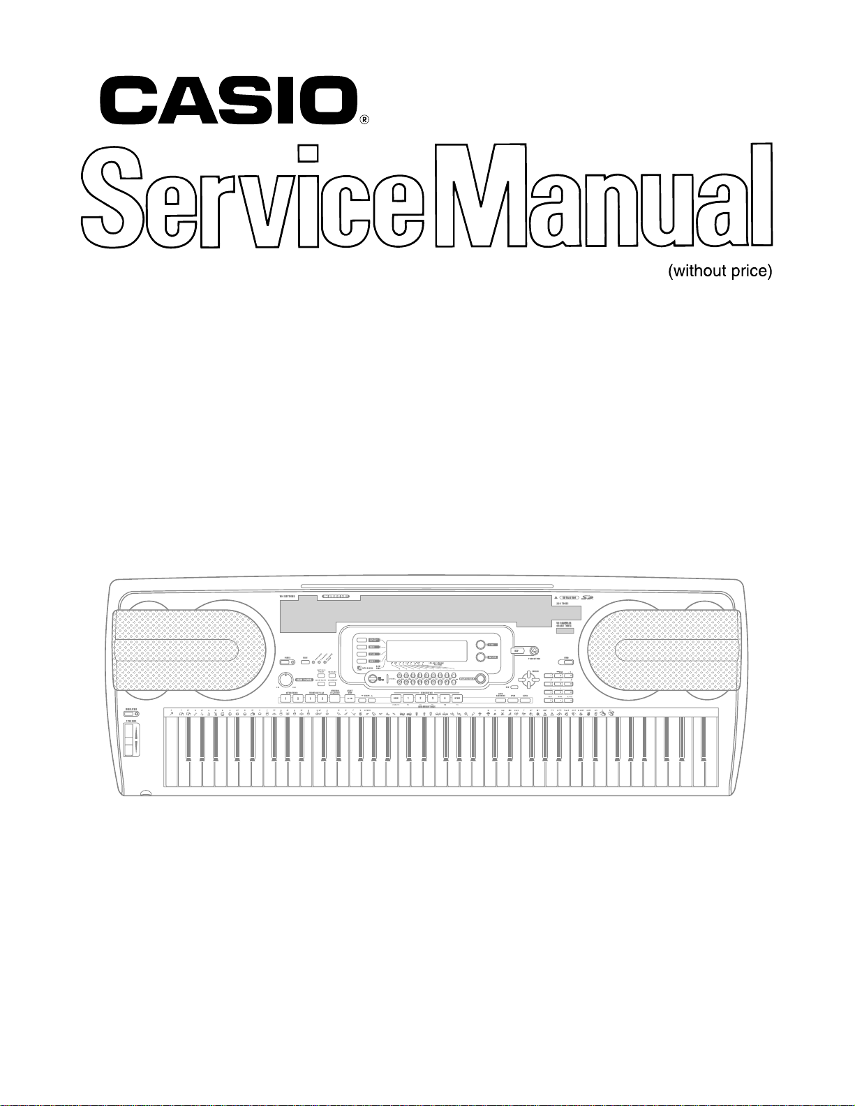
WK-3300
JUL. 2006
ELECTRONIC KEYBOARD
WK-3300
Page 2

CONTENTS
SPECIFICATIONS ----------------------------------------------------------------------------------------- 1
BLOCK DIAGRAM ---------------------------------------------------------------------------------------- 3
CIRCUIT DESCRIPTION--------------------------------------------------------------------------------- 4
PRINTED CIRCUIT BOARD ---------------------------------------------------------------------------- 6
DISASSEMBLY--------------------------------------------------------------------------------------------11
DIAGNOSTIC PROGRAM----------------------------------------------------------------------------- 17
EXPLODED VIEW --------------------------------------------------------------------------------------- 20
PARTS LIST ----------------------------------------------------------------------------------------------- 21
SCHEMATIC DIAGRAMS ----------------------------------------------------------------------------- 25
Page 3
SPECIFICATIONS
GENERAL
Keyboard: 76 keys with touch response (OFF/1/2/3)
Tones: 400 Advanced Tones + 200 Preset Tones + 20 Drum Sets + 100 standard user tones
+ 20 user tones with waves*1 + 4 user drum sets with waves*1 + 50 drawbar organ
tones + 100 user drawbar organ tones (894 tones total); layer/split
Polyphony: 32 notes maximum (10 for certain tones)
Drawbar Organ Function
Drawbars: 9 (16’, 5 1/3’, 8’, 4’, 2 2/3’, 2’, 1 3/5’, 1 1/3’, 1’)
Percussion: Second, Third
Click: On, Off
Effects: DSP (200 types: internal, 100 user areas) + Reverb (16 types) + Chorus (16 types) +
Equalizer (10 types, 4 bands)
Auto Accompaniment
Rhythm Patterns: 182 (internal, 16 user areas*1 )
Tempo: Variable (226 steps, = 30 to 255)
Chords: 3 fingering methods (CASIO CHORD, FINGERED, FULL RANGE CHORD)
Rhythm Controller: START/STOP, INTRO/ENDING 1 and 2, VARIATION/FILL-IN 1 and 2, SYNCHRO/
FILL-IN NEXT
Accomp Volume: 0 to 127 (128 steps)
One-touch Presets: Recalls settings for tone, tempo, layer on/off, and harmonize on/off in accordance
with rhythm.
Auto Harmonize: 10 types : Automatic addition of notes that harmonize with melody note in accordance
with specified Auto Accompaniment chords.
Memory Function
Songs: 5
Recording Tracks: 6 (2 through 6 are melody tracks)
Recording Methods: Real-time, step
Memory Capacity: Approximately 10,000 notes (total for 5 songs)
Edit Function: Equipped
Demo Tunes: 3
Tune Number Name Composer
0 Island Dusk TECH-NOTE INTERNATIONAL LTD.
1 Malibu Sun TECH-NOTE INTERNATIONAL LTD.
2 Ticket to Cambridge TECH-NOTE INTERNATIONAL LTD.
Synthesizer Function
Parameters: Attack time; release time; resonance; cutoff frequency; vibrato type; vibrato delay;
vibrato depth; vibrato rate; octave shift; level; touch sense; reverb send; chorus send;
DSP line; DSP type; DSP parameter; Modulation Assign; Modulation Depth
Registration Memory
Number of Setups: 32 (4 setups ✕ 8 banks)
Memory Contents: Tone, Rhythm, Tempo, Layer on/off, Split on/off, Split point, Harmonize on/ off, Mixer
settings (Channels 1 to 10), Effect settings, Touch Response settings, Assignable
jack setting, Transpose, Tuning, Accompaniment volume setting, Pitch bend range,
Auto Harmonize type, MODE button setting, Synchro standby state, Mixer Hold, DSP
Hold, Synthesizer Mode parameters
Mixer Function
Channels: 16
Parameters: Tone; part on/off; volume; pan pot; octave shift; coarse tune; fine tune; reverb send;
chorus send; DSP line; DSP level, DSP pan, DSP system reverb send, DSP system
chorus send
MIDI: 16 multi-timbre receive, GM Level 1 standard
— 1 —
Page 4

Other Functions
Pitch Bend Range: Adjustable (12 semitones upwards and downwards)
Modulation: Equipped
Transpose: 49 steps (–24 semitones to +24 semitones)
Tuning: Variable (A4 = approximately 440Hz ±100 cents)
LCD: Adjustable contrast
SMF Player: Flash memory storage for up to 200 files*
1
Supported Format: SMF0
Flash Memory
Capacity: 4MB*
2
Shared Area: Approximately 3.5MB*2 (waveform data, accompaniment data, SMF data)
Further storage of waveform, accompaniment, and SMF data becomes impossible
after the total of such data reaches approximately 3.5MB.
SD Memory Cards
Supported SD Memory Cards
: 1GB or less (Cards with capacity greater than 1 GB are not supported.)
Functions: Save and load of user tones, user songs, and registration data; playback of SMF; card
formatting; file delete; file rename
Terminals
SD memory card slot
USB port: TYPE B
Sustain/Assignable Terminal
Headphone/Output Terminal
: Standard jack (sustain, sostenuto, soft, rhythm start/stop)
: Stereo standard jack
Output Impedance: 200Ω
Output Voltage: 5.5V (RMS) MAX
Power Supply Terminal: 12V DC
Power Supply: Dual power supply system
Batteries: 6 D-size batteries
Battery Life: Approximately 4 hours continuous operation on alkaline batteries
AC Adaptor: AD-12
Auto Power Off: Turns power off approximately six minutes after last key operation. Enabled under
battery power only, can be disabled manually.
Speaker Output: 6.1W + 6.1W
Power consumption: 12V 18W
Dimensions: 122.3 ✕ 42.3 ✕ 16.0cm (48
3
/
16
✕ 16
11
/
✕ 6
16
5
/16 inch)
Weight: Approximately 10.0kg (22.0 lbs) (without batteries)
*1 The same memory area is used to store waveform data, accompaniment data, and SMF data.
*2 Noted capacities are calculated values based on 1MB = 10242 bytes.
ELECTRICAL
Current drain with 12 V DC:
Consumption Current 1720 mA ± 20 %
Consumption Current at idle 290 mA ± 20 %
with 12 keys from F3 to E4 pressed in 479 Ocarinag + LAYER
Volume: maximum, Velocity: maximum
Speaker output level (Vrms with 8 Ω load each channel):
with key L(E1)/R(G1) in 479 Ocarinag
Volume: maximun, Velocity: maximum L: 5700 mV ± 20 %
R: 5670 mV ± 20 %
Phone output level (Vrms with 32 Ω load each channel):
with key L(C2)/R(B5) in 479 Ocarinag
Volume: maximun, Velocity: maximum L: 360 mV ± 20 %
R: 330 mV ± 20 %
Output level (Vrms with 47 KΩ load each channel):
with key L(E1)/R(G1) in 479 Ocarinag
Volume: maximun, Velocity: maximum L: 3100 mV ± 20 %
R: 3030 mV ± 20 %
— 2 —
Page 5
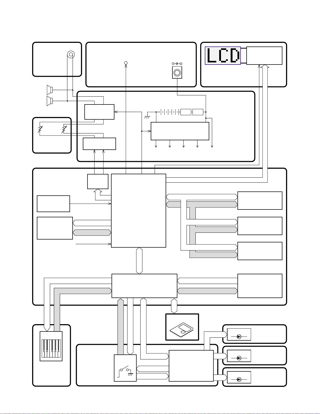
BLOCK DIAGRAM
Phones/Output
CONSOLE PCB
(M740-CNA3)
Speakers
(R)
(L)
Main
Volume
CONSOLE PCB
(M740-CNA2)
MAIN PCB
(M740-MDA1)
Reset IC
IC6
R1151N001C-TR
LOUT
RESET
SUB PCB (M740-PSA2)
Assingnable Jack
Power Amplifier
IC205
LA4636
Filter
IC202, NJM2008D
ROUT
DAC IC1
uPD63200GS
APO
MPU
IC13
AC ADAPTOR
DC 12V
Battery
Power Supply Circuit
Q201 ~ Q204,
IC201, D205, D206
(9-12V)
VC
(5V)
VD5
D214
(5V)
VF5
LCD PCB
(M734-LCD1M)
D201
(9-12V)
(5V)
VCP
VA5
SUB PCB
(M740-PSA1)
MA0 ~ MA20
MD0 ~ MD15
LCD Controller
ML9040-B02GA (IC401)
CONT
E
R/W
RS
FLASH ROM (32MBit)
LH28F320BFHE
DB0 ~ DB7
IC11
RAM (1Mbit)
IC5
CY62128DV30LL
SI0 ~ SI9, FI0 ~ FI9
Keyboard
Keyboard PCBs
(M764T-KY1M/
KY2M)
EA0 ~ EA15, EA18
ED12 ~ ED19
16.384MHz
KC0 ~ KC7
CONSOLE PCB
(M740-CNA1)
uPD914AGM-JED
ARXD
ATXD
ZX-BUSYB
SYSRSTB
BEND
MOD
KEY/BUTTON/SD CARD
CONTROLLER
IC20
TC190C020AF-001
KC3 ~ KC7
FI10, KI0 ~ KI2
Buttons
PWSW
RESB
TXDO
TXDI
SWIO ~ SWI7
SWCO ~ SWC6
MA0 ~ MA16, MA25
A1 ~ A17
D0 ~ D15
Smart media Unit
BUTTON/LED
CONTROLLER
IC301
UPD65881GK-1019ETA
MA0 ~ MA21
MD0 ~ MD15
MD0 ~ MD7
DATA ACCESS
ROM (128Mbit)
MR27T12800LO
RAM (2Mbit)
LP62S2048X-70LLT/Q
RAM (128 x 16bit)
LP62S16128BV
DSP
DRAWBER
IC10
IC7
IC23
CONSOLE PCB
(M740-CNA4)
CONSOLE PCB
(M740-CNA5)
CONSOLE PCB
(M740-CNA6)
— 3 —
Page 6
CIRCUIT DESCRIPTION
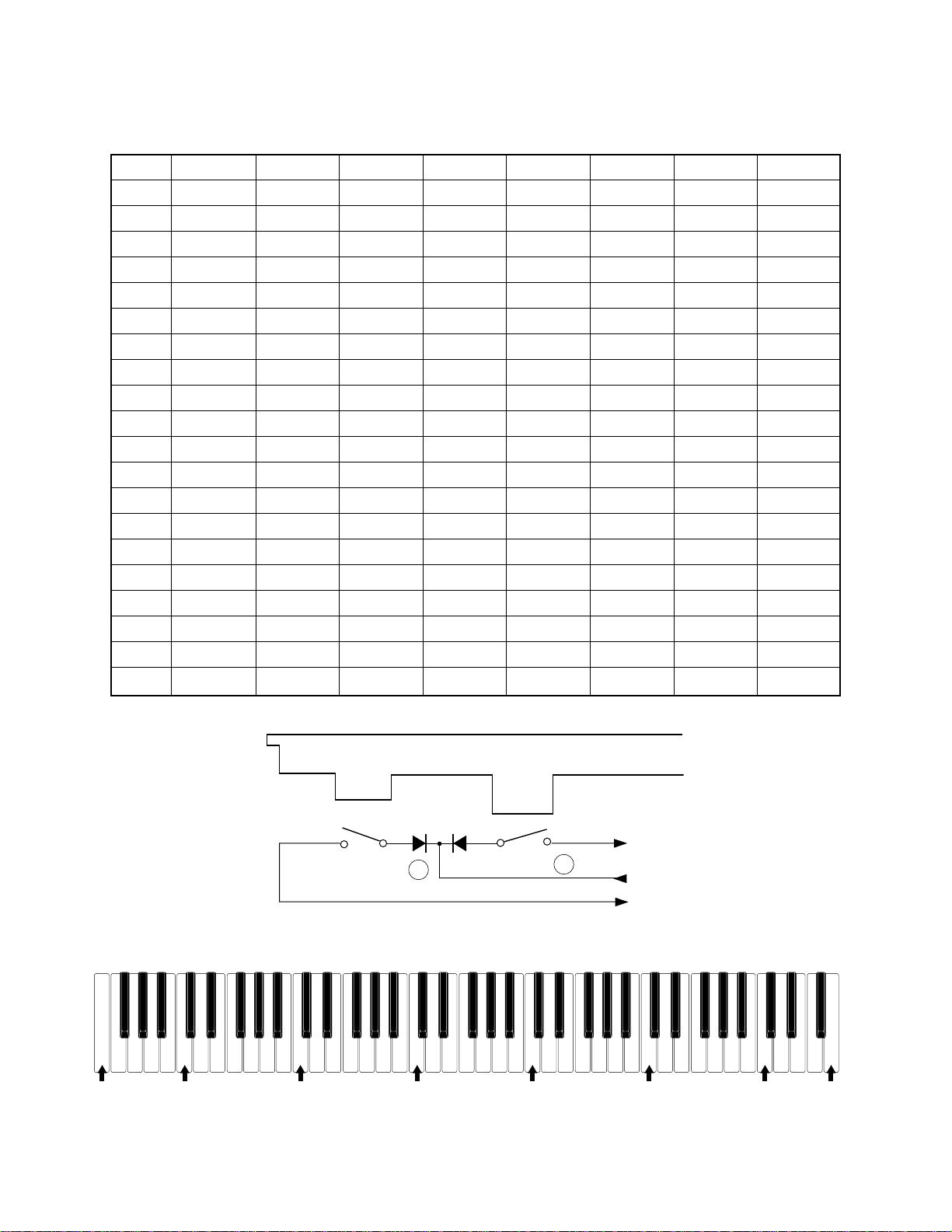
KEY MATRIX
KC0 KC1 KC2 KC3 KC4 KC5 KC6 KC7
FI0 E11 F11 F#11 G11 G#11 A11 A#11
SI0 E12 F12 F#12 G12 G#12 A12 A#12
FI1 B11 C21 C#21 D21 D#21 E21 F21 F#21
SI1 B12 C22 C#22 D22 D#22 E22 F22 F#22
FI2 G21 G#21 A21 A#21 B21 C31 C#31 D31
SI2 G22 G#22 A22 A#22 B22 C32 C#32 D32
FI3 D#31 E31 F31 F#31 G31 G#31 A31 A#31
SI3 D#32 E32 F32 F#32 G32 G#32 A32 A#32
FI4 B31 C41 C#41 D41 D#41 E41 F41 F#41
SI4 B32 C42 C#42 D42 D#42 E42 F42 F#42
FI5 G41 G#41 A41 A#41 B41 C51 C#51 D51
SI5 G42 G#42 A42 A#42 B42 C52 C#52 D52
FI6 D#51 E51 F51 F#51 G51 G#51 A51 A#51
SI6 D#52 E52 F52 F#52 G52 G#52 A52 A#52
FI7 B51 C61 C#61 D61 D#61 E61 F61 F#61
SI7 B52 C62 C#62 D62 D#62 E62 F62 F#62
FI8 G61 G#61 A61 A#61 B61 C71 C#71 D71
SI8 G62 G#62 A62 A#62 B62 C72 C#72 D72
FI9 D#71 E71 F71 F#71 G71
SI9 D#72 E72 F72 F#72 G72
Note: Each key has two contacts, the first conatct 1 and second contact 2.
Key
Second contact
2
First contact
1
NOMENCLATURE OF KEYS
C2 C3 C4 C5 C6 C7 G7E1
FI
KC
SI
— 4 —
Page 7
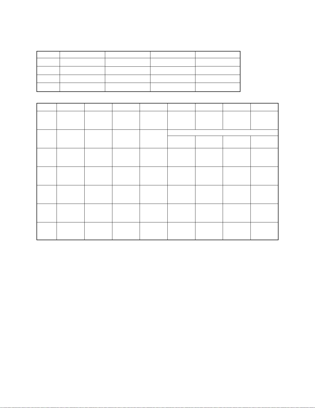
BUTTON MATRIX
KC4
KC5
KC6
KC7
SWC0
SWC1
SWC2
SWC3
SWC4
KI0
LAYER
2
5
9
SWI0
ACCOMP
VOLUME
SONG
MEMORY
CARD
CH1
TRANCEPOSE/
FUNCTION
SWI1
ONE
TOUCH
PRESET
TEMPO
DOWN
SMF
PLAYER
CH2
MIXER
KI1
SPLIT
–
4
8
SWI2
MODE
START/
STOP
TEMPO
UP
CH3
SYNTH
KI2
AUTO HARMONIZE
0
1
7
SWI3
INTRO/
ENDING 1
BANK
CH9
CH4
EFFECT
ENDING 2
FI10
+
3
6
DEMO
SWI4
INTRO/
REGISTRATION/SONG MEMORY TRACK
1
CH10
CH5
CH6
SWI5
VARIATION/
FILL-IN 1
2
CH11
CH14
CH7
SWI6
VARIATION/
FILL-IN 2
3
CH12
CH15
CH8
1 FEET UP
SWI7
SYNCRO/
FILL-IN
NEXT
4
CH13
CH16
SWC5
SWC6
RHYTHM
TONE
1 FEET
DOWN
PIANO
SETTING
STORE
ORGAN
DSP
EXIT
씰
씱
쑼
쑿
— 5 —
Page 8
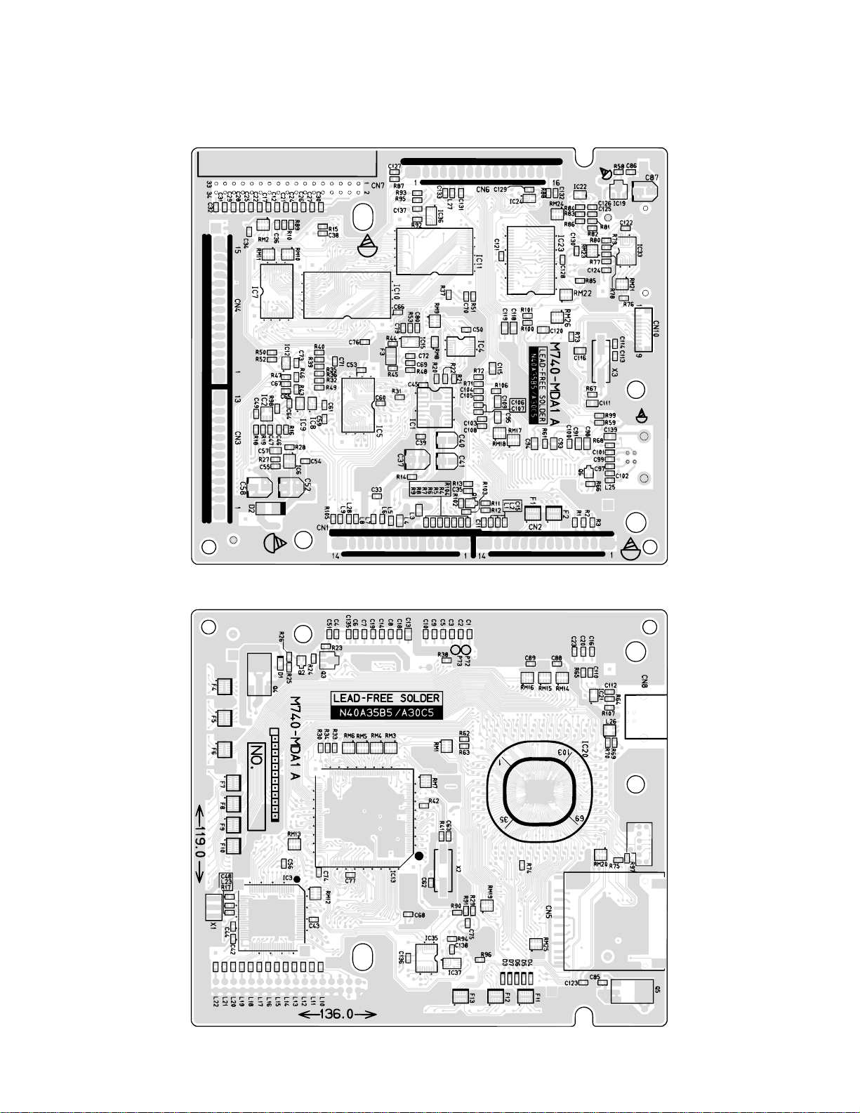
MAIN PCB M740-MDA1
PRINTED CIRCUIT BOARD
Top View
Bottom View
— 6 —
Page 9
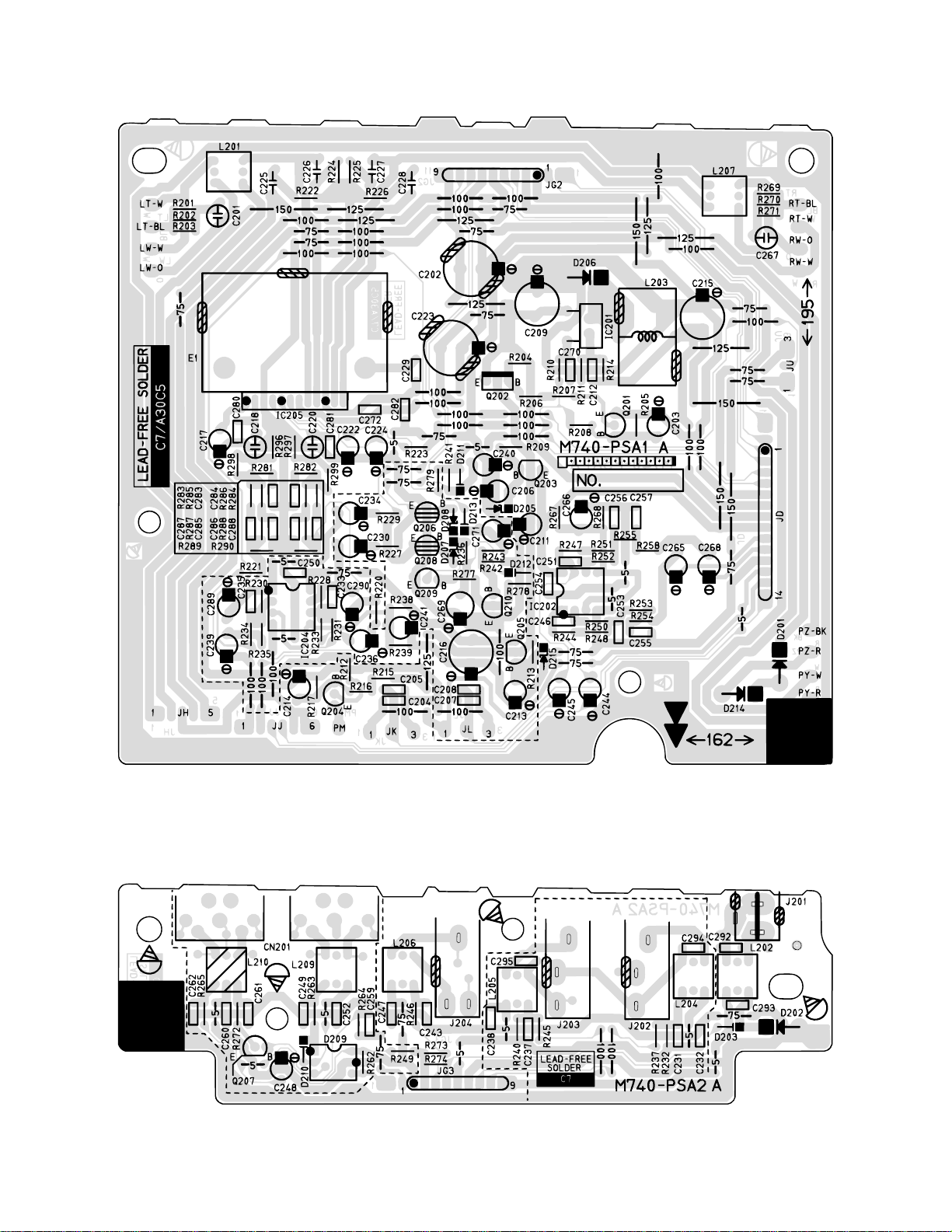
SUB PCB M740-PSA1
SUB PCB M740-PSA2
Top View
Top View
— 7 —
Page 10
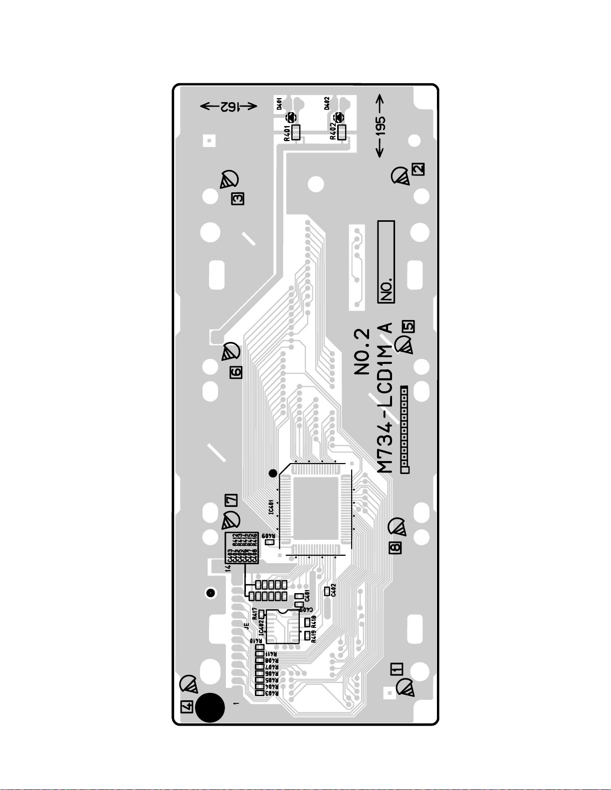
DISPLAY PCB M734-LCD1M
Top View
— 8 —
Page 11
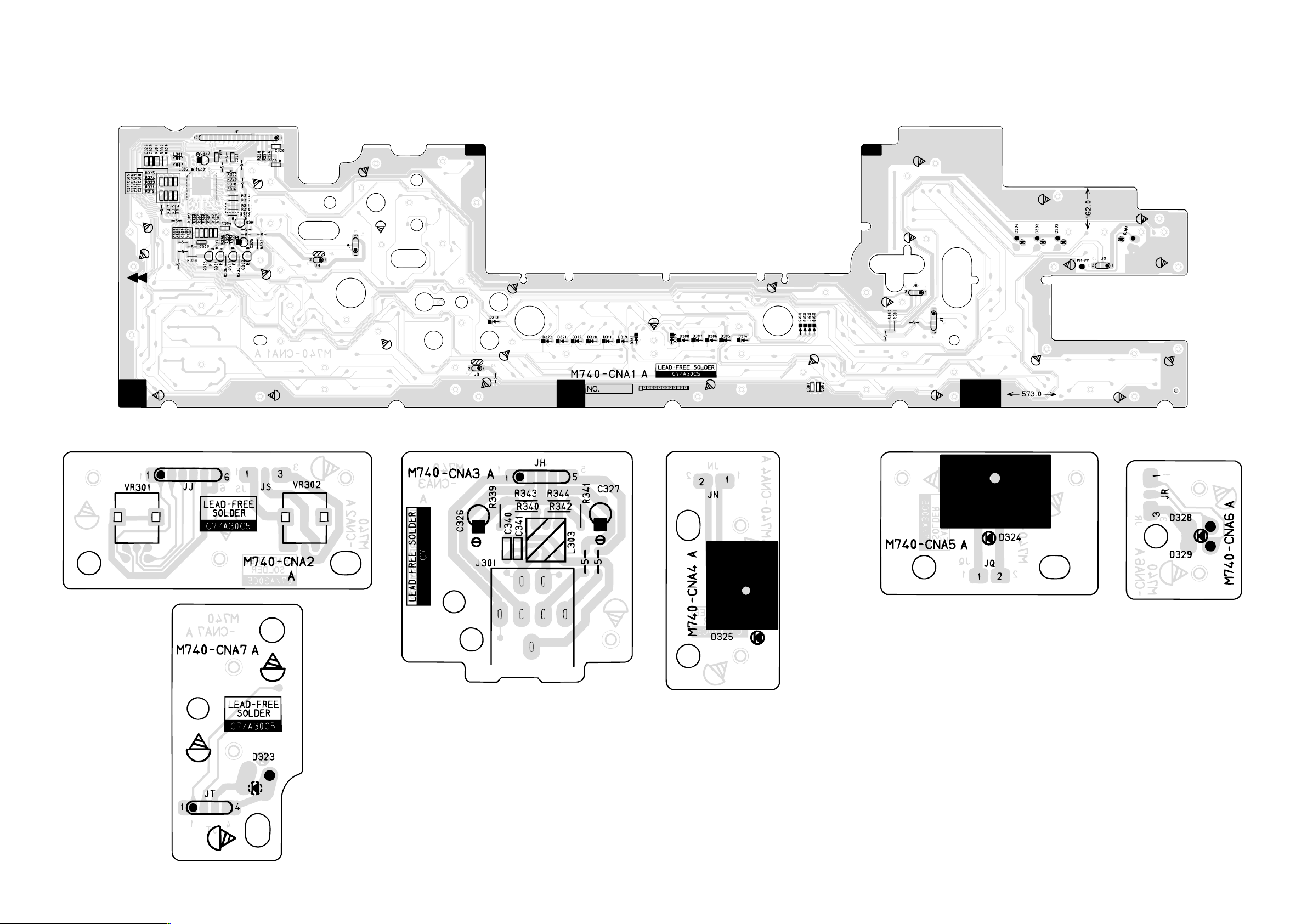
CONSOLE PCB M740-CNA1
CONSOLE PCB
M740-CNA7
CONSOLE PCB M740-CNA4CONSOLE PCB M740-CNA3CONSOLE PCB M740-CNA2 CONSOLE PCB M740-CNA5 CONSOLE PCB
M740-CNA6
— 9 —
Page 12
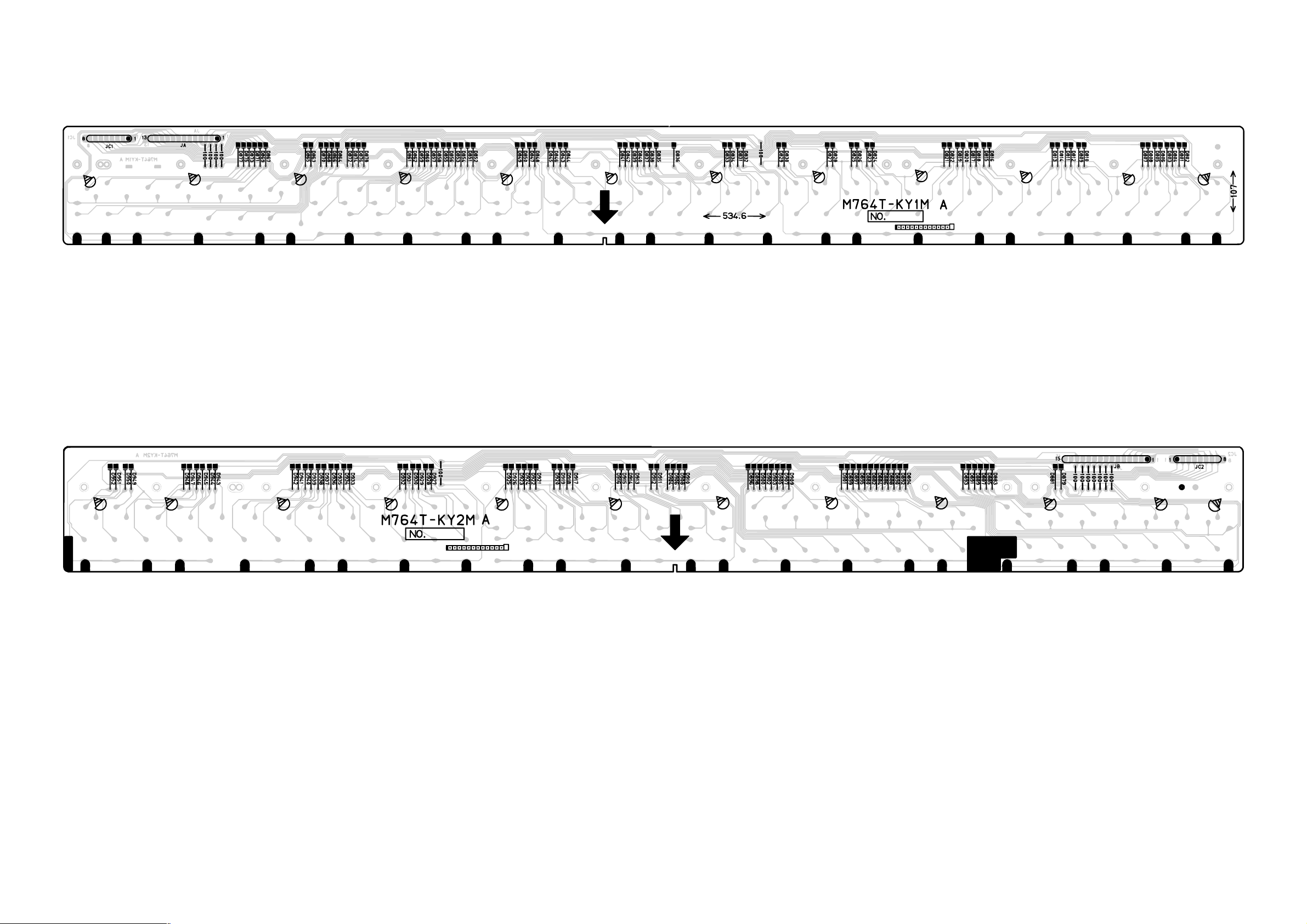
KEYBORD PCB M764T-KY1M
KEYBORD PCB M764T-KY2M
— 10 —
Page 13
DISASSEMBLY
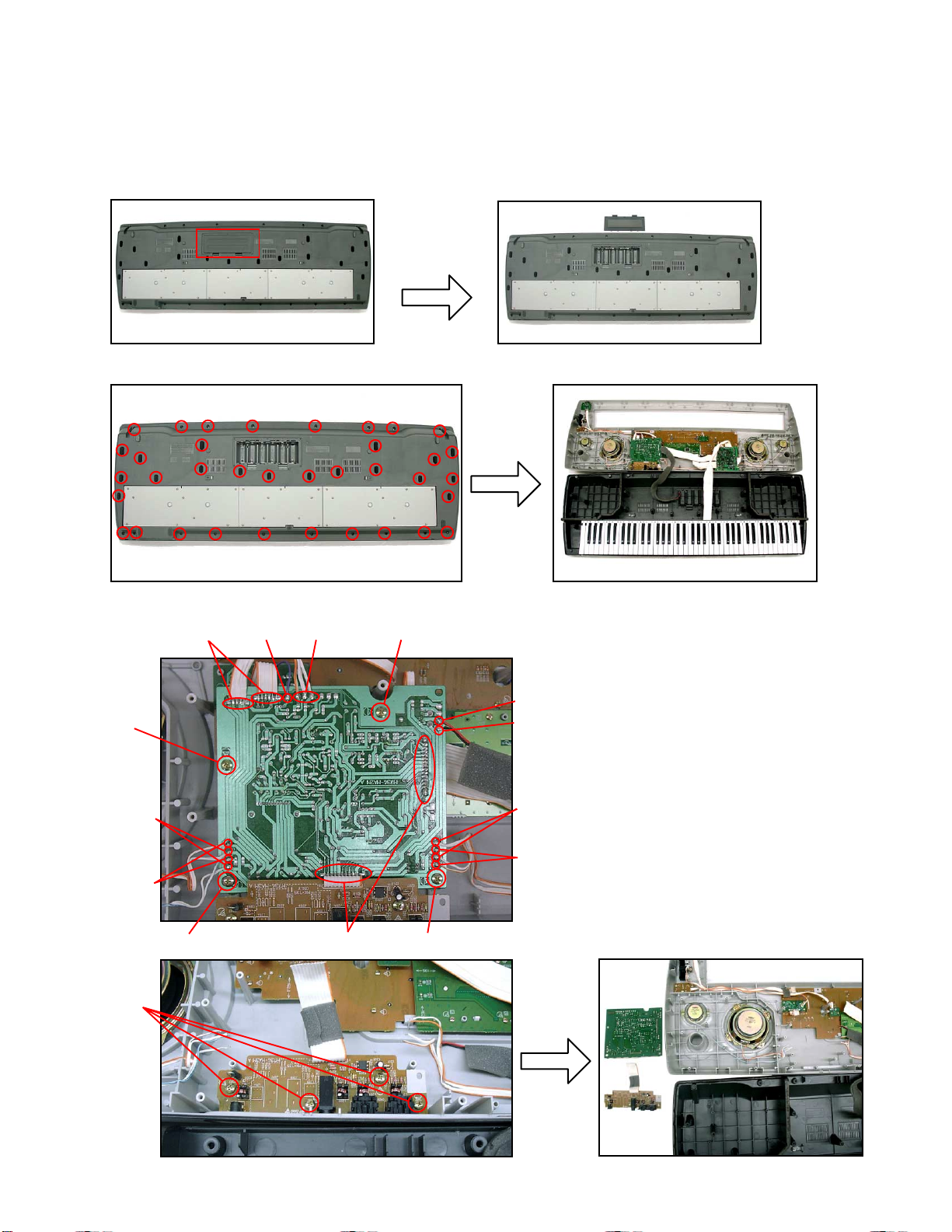
■ The Disassembly Procedure inscribed on this manual is exactly the same as that of
WK-3200 since WK-3300 has the same frame as WK-3200.
1. Remove the battery cover and then the battery.
2. Remove 36 screws and then the upper case.
3.
Remove 4 screws, 8 speaker cords, 2 battery cords, 1cord (PM), 5 connectors (JD, JG2, JH, JK, JJ) and then the PCB ASS'Y (MA2M).
Connectors
Screw
Speaker
cords (W)
Speaker
cords (O)
Screws
Screw
ConnectorCord
Connectors
Screw
Battery cord (R)
Battery cord (B)
Speaker cords (W)
Speaker cords (O)
Screw
— 11 —
Page 14
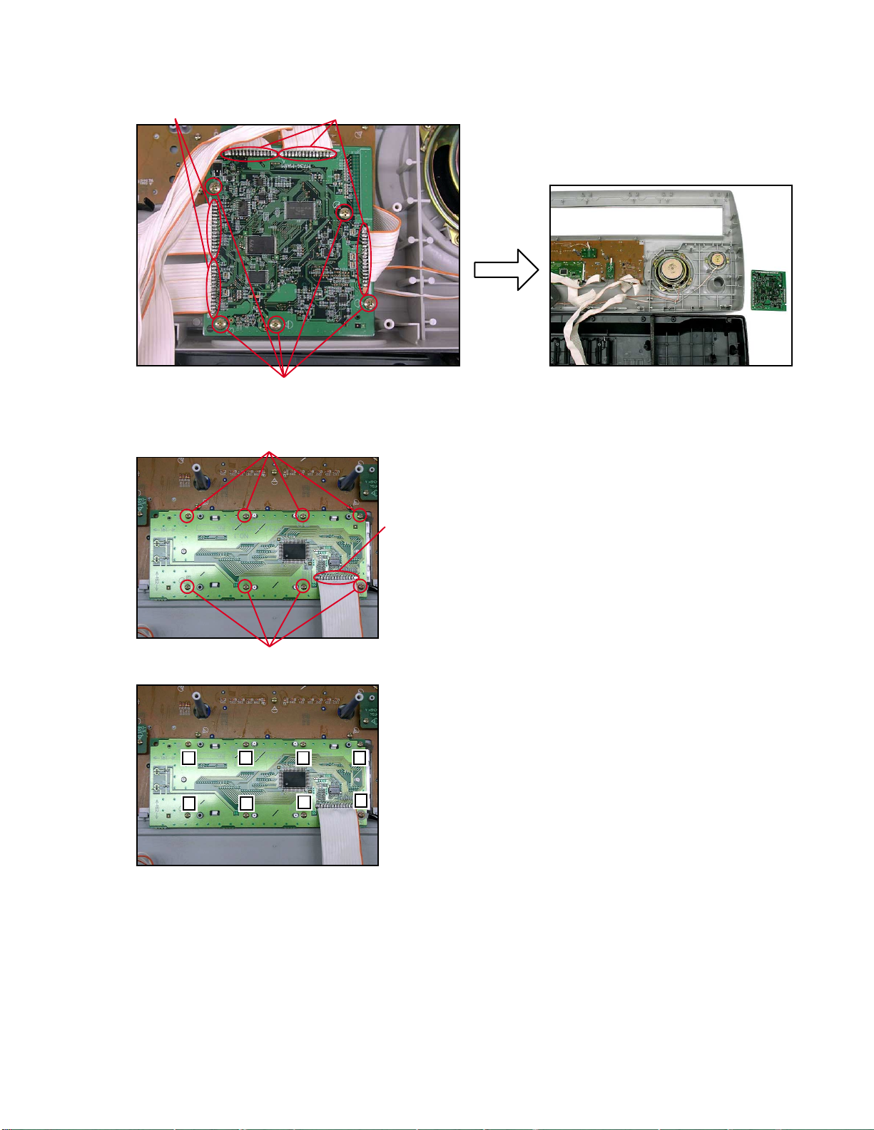
4. Remove 5 screws, 5 connectors (JA, JB, JD, JE, JF) and then the PCB ASS'Y (MA1M).
ConnectorsConnectors
Screws
5. Remove 8 screws, 1 connector and then the LCD ASS'Y (LCD1M).
Screws
Connector
Screws
1852
3
6
7
4
Note: Tighten the screws in the order from 1 to 8 when
reassembling.
— 12 —
Page 15
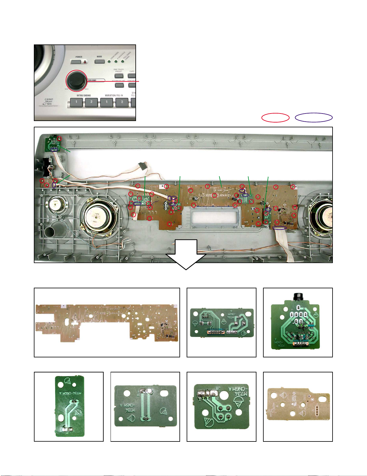
6. Remove the volume knob, screws, connectors and then the CN1, CN2, CN3, CN4, CN5, CN6, CN7.
Volume knob
CN1M
CN3M
CN7M
CN2M
Screws
CN1MCN2M CN6M CN5M CN6M
CN3M
Connector
CN5MCN4M
CN6M CN7M
— 13 —
Page 16
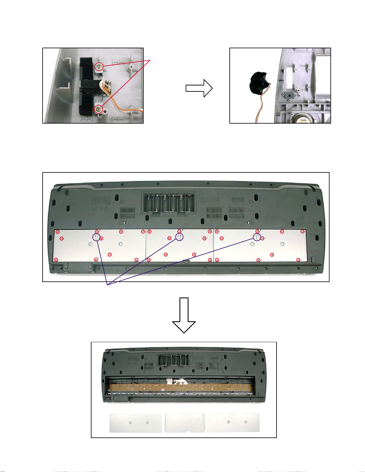
7. Remove 2 screws and then the Bender assy.
Screws
8. Remove 29 screws and then the lower case.
Note: Tighten the screw with the arrow mark in the figure first when reassembling.
— 14 —
Page 17
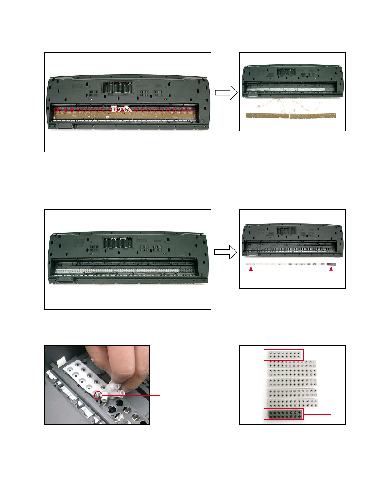
9. Remove 24 screws and then the PCB ASSY (KY1M, KY2M).
10.Remove the rubber keys.
Projection
Note: Pay attention to the positions of the rubber keys as one of them has a different length.
Match the projections of the rubber keys with the holes of the lower case when reassembling.
— 15 —
Page 18
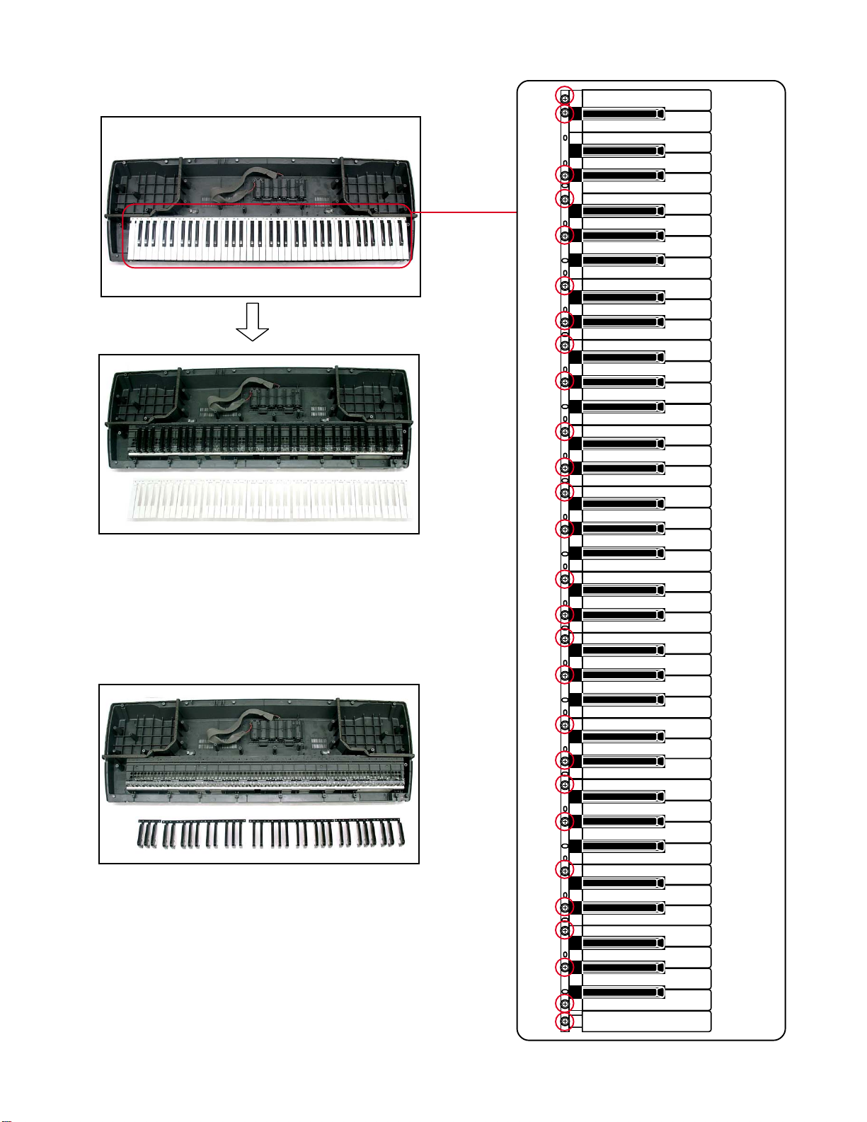
11.Remove 27 screws and then the white keys.
Note: Pay attention to the positions of the screw holes when
reassembling.
12.Remove the black keys.
— 16 —
Page 19
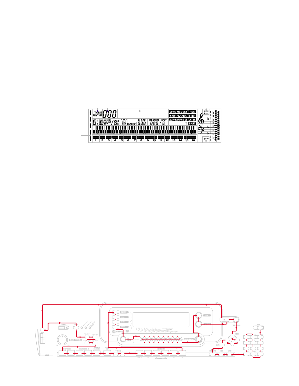
DIAGNOSTIC PROGRAM
8 7
BCD A 60 9
■ Initial Setup
1. Connect an AC adaptor.
2. Connect a Sustain pedal.
3. "Main" volume: MAX.
4. Insert the SD card.
■ How to start diagnostic program
1. Press the “POWER” button while pressing the “Cursor key Up” and “Cursor key Down” buttons.
2. Release the “POWER” button first while still pressing the “Cursor key UP” and “Cursor key Down” buttons.
3. Release the “Cursor key UP” and “Cursor key Down” buttons. “TEST 740” appears on the LCD.
NOTE:
Refer to the figure below for the LCD messages that appear during the diagnostic program.
3
2
514
Gran ndP o
E
■Diagnostic program
1. Button check
1 Press “DSP” button.
2 Press buttons in the following order.
NOTE: NG sound sounds when a button is defective or buttons are pressed in a wrong order.
LCD message appears in the area 1.
Message on LCD Message on LCD Message on LCD Message on LCD
1 DSP
2 MODULATION
3 MODE
ONE TOUCH PRESET
4
5 CARD
ACCOMP VOLUME
6
7 SONG MEMORY
8 INTRO/ENDING 1
9 INTRO/ENDING 2
VARIATION/FILL-IN 1
@
A
VARIATION/FILL-IN 2
B
SYNCHRO/FILL-IN NEXT
C START/STOP
D TEMPO쑼
E TEMPO쑿
F BANK
G REGISTRATION 1
H REGISTRATION 2
MOD
MODE
OTP
CARD
ACMP VOL
SONG
INT/END1
INT/END2
VAR/FIL 1
VAR/FIL 2
SYNCHRO
STRT/STP
TEMPO/DW
TEMPO/UP
BANK
REGIST 1
REGIST 2
I REGISTRATION 3
J REGISTRATION 4
K STORE
TRANSPOSE/FUNCTION
L
M MIXER
N SYNTH
O EFFECT
P SMF PLAYER
Q CH1
R CH2
S CH3
T CH4
U CH5
V CH6
W CH7
X CH8
Y 1Ft UP
Z CH9
REGIST 3
REGIST 4
STORE
TRN/FUNC
MIXER
SYNTH
EFFECT
SMF
CH1
CH2
CH3
CH4
CH5
CH6
CH7
CH8
1Ft UP
CH9
[ CH10
\ CH11
] CH12
_ CH13
a CH14
b CH15
c CH16
d DSP CH
DRAWBAR ORGAN
e
f TONE
g RHYTHM
h DSP
i PIANO SETTING
j [CURSOR BUTTONS]
UP
k RIGHT
l DOWN
m LEFT
CH10
CH11
CH12
CH13
CH14
CH15
CH16
DSP CH
DRAWBAR
TONE
RHYTHM
DSP
PIANO
UP
RIGHT
DOWN
LEFT
n EXIT
AUTO HARMONIZE
o
p SPLIT
q LAYER
r 0
s 1
t 4
u 7
v 8
w 5
x 2
y z +
{ 3
| 6
} 9
~ DEMO
EXIT
HARMO
SPLIT
LAYER
0
1
4
7
8
5
2
+
3
6
9
DEMO
SW OK
2
3
8 9 0 A B C
4
6
5
7
L
M
N
O
P
D E
QRSTU V W X Y
Z[\]^ a b c d
F G H I J K
— 17 —
f
g
e
o
1
h i
m
n
p q
j
l
k
t
s
r
~
vu
}
w
|
x {
zy
Page 20

2. AC adaptor detection check.
1 Press “TONE” button.
2 When the instrument detects that an AC adaptor is plugged in, an OK sound
sounds. “ACJ OFF” appears and an NG sound sounds when the AC adaptor
is not plugged (when batteries are used).
3. Sustain jack check. (If no pedal, this check can be skipped)
1 Press “RHYTHM” button.
2 Press “Sustain pedal” .
3 Release “Sustain pedal” .
4 NG sound, “OFF” sound this case, must be audible.
4. Low Voltage detection check.
1 Press “DRAWBAR ORGAN” button.
2 OK sound must be audible.
5. Sound Source check
1 Press “7” button.
2 The MAX sin sound sounds from Left spesker.
3 Press “8” button.
4 The MAX sin sound sounds from Both spesker.
5 Press “9” button.
6 The MAX sin sound sounds from Right spesker.
Message on LCD
1 ACJ ON
1 SUS CHK
1 SUS ON
1 SUS OFF
1 VOLT HI
1 TG MAX L
1 TG MAX C
1 TG MAX R
6. ROM check
1 Press “INTRO/ENDING1” button.
7. Flash memory check
1 Press “INTRO/ENDING2” button.
8. Flash memory SUM check
1 Press “SONG MEMORY” button.
9. DSP RAM check
1 Press “VARIATION/FILL-IN 2” button
10. CPU RAM check
1 Press “SYNCHRO/FILL-IN NEXT” button.
1 ROM CHK
앗
1 ROM OK
1 FMC CHK
앗
1 FMC OK
1 FMS CHK
앗
1 FMS 7898
1 DRAM OK
1 CRAM OK
— 18 —
Page 21

11. LED check
1 Press “TEMPO쑼” button.
2 LEDs illuminate in the following order.
MODULATION
FULL RANGE CHORD
FINGERED
CASIO CHORD
DATA ACCESS
DRAWBAR ORGAN
DSP
12. LCD check
1 Press “TEMPO쑿” button.
2 Turn on all segments of the LCD.
13. Card check (If no smart media card, this check can be skipped)
1 Press “-” button.
“Err NO CARD” appears and an NG sound sounds when no card is inserted.
14. Bender check
1 Press “MODE” button.
2 Turn the “PITCH BEND WHEEL” to MAX.
3 Turn the “PITCH BEND WHEEL” to MIN.
Message on LCD
1 LED CHK
앗
앗
앗
앗
앗
앗
앗
앗
1 LED END
1 SMC CHK
앗
1 CARD OK
1 BEND CHK
2 127
1 BEND CHK
2 000
1 BEND OK
15. TUNE check (If no TUNING METER, this check can be skipped)
1 Connect the TUNING METER to the phone jack.
2 Press “8” button.
3 The TUNING METER must indicate "C".
4 Disconnect the TUNING METER from the phone jack.
16. APO check
1 Press “EXIT” button.
* Go out from TEST mode (Power off).
* The LCD turns off.
DIAGNOSTIC PROGRAM IS FINISHED.
1 Exiting
— 19 —
Page 22
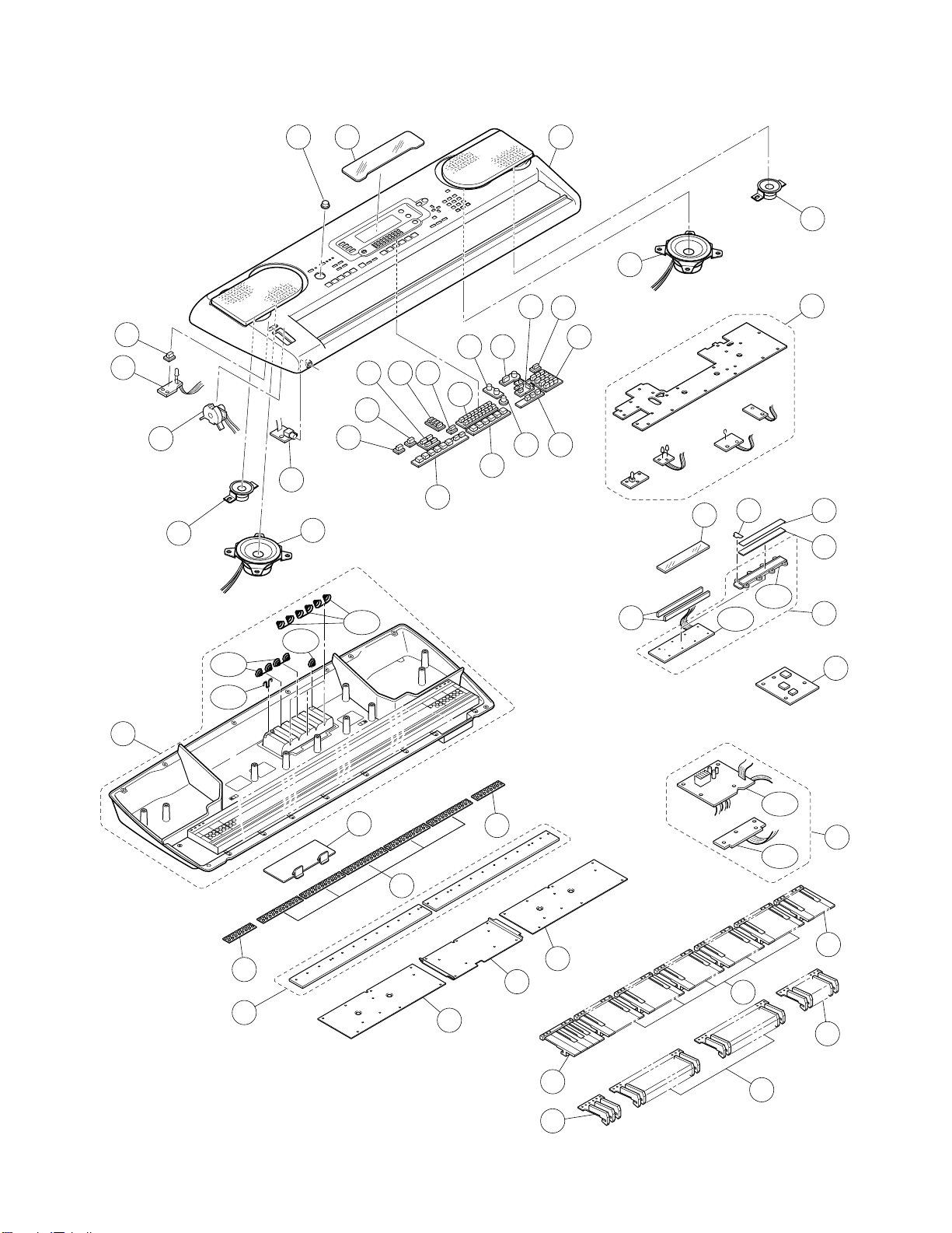
EXPLODED VIEW
26
3
25
19
3
17
16 40
33
28 29 30
32
26
39
31
27
18
36
37
3534
26
38
18
20
23
19
3
22
21
41
41-3
41-1
12
14
41-2
41-4
15
11
43
13
42
43
24
4-2
4-1
4
1
PSA1
2
PSA2
6
5
9
— 20 —
10
7
8
Page 23

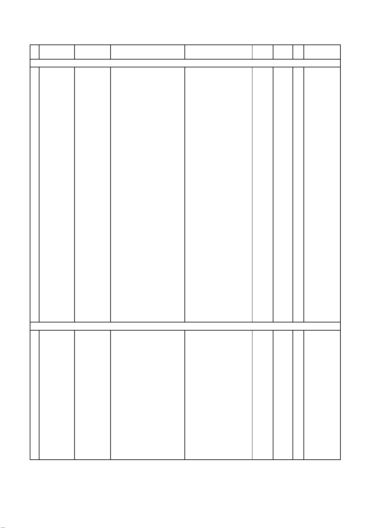
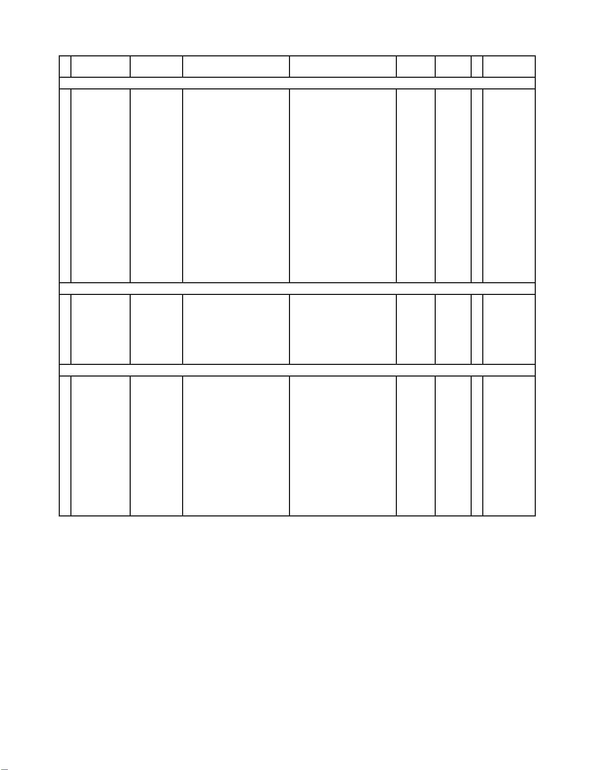
PARTS LIST
WK-3300
Notes: This parts list does not include the cosmetic parts,
which parts are marked with item No. "R-X" in the
exploded view.
Contact our spare parts department if you need
these parts for refurbish.
1. Prices and specifications are subject to change
without prior notice.
2. As for spare parts order and supply, refer to the
"GUIDEBOOK for Spare parts Supply",
published seperately.
3. The numbers in item column correspond to the
same numbers in drawing.
— 21 —
Page 24
N Item Code No. Part Name Specification Overs
K
X
Q
F
Main PCB MA1M
N1
IC2
IC4 10197802
IC5 10198126
N
N
N
N
N
N
IC6 10241413
IC7 10197390
IC8,9,21,22 10197555
IC13 10200257
IC15 10197809
IC19 10239682
IC33 10240648
IC35 10197798
IC36 10245659
IC37 10245660
Q3 10197813
Q1,2 69300298
Q4,5 10015566
D1 10199220
D2 23902058
D3-7 10009218
L3 10214942
L1,2,59,27,28
L26
L4
L24,25
Q6
F6,7,8
F1,2,4,5,9-13
X2
X3
10248134
10197796
PCB ASSY/MAIN TK-RJM507144*001 1 DT A
IC TA75S393F(TE85L.F) 1 AL C
IC TC74VHCT08AFT(EL.
LSI CY62128DV30LL70ZA
IC R1151N001C-TR-F
LSI LP62S2048AX70LLTF
IC TC7SZ14FU(TE85L.F)
IC UPD914AGM-JED-A
IC
TC7WH123FU(TE12L.
IC RH5RL33AA-T1-F
IC TC74LCX08FT(EL.K)
IC TC74LCX138FT(EL.K)
IC TC7WZ00FU(TE12L.F)
IC TC7WZ08FU(TE12L.F)
TRANSISTOR 2SD2150T100R
TRANSISTOR 2SC4081T106R
TRANSISTOR 2SB1181TLR
DIODE HZU4.3B2TRF-E
DIODE 1SR154-400TE25
DIODE 1SS400TE61
COIL BLM21PG331SN1D
1AEC
1BNC
1AEC
1AYC
4AEC
1CHC
1AEC
1ABC
1AEC
1AIC
1AFC
1AGC
1AEC
2AAC
2ACC
1ABC
1AAC
5AAC
1AAC
10095204 COIL BLM18AG102SN1D 9 AA C
10158809 COIL DLP31SN221SL2L 1 AI C
10122963 COIL BLM21AG102SN1D 1 AC C
10089941 COIL BLM21PG221SN1D 2 AA C
10153685 FET 2SJ346(TE85L.F) 1 AA C
10122975 R-C NETWORK EZASSB516BJ 3 AA C
10122976 R-C NETWORK EZASTB63ABJ 9 AA C
10208977 RESONATOR SSM1638400F16FSFZ81ACC
10211946 RESONATOR SSM1200000F17F5FZ81ACC
Price
Code
R Remarks
N2
IC201
IC202
IC205
Q201,203,
204,205
D201,202,20
6,214
Q202
D203
D205
J201
J204
L201,202,20
6,207
L203
Sub PCB MA2M
10248136
10201503
10206677
10203081
PCB ASSY/PSA TK-RJM507145*001 1 CL B
IC PQ1CG21H2FZH
IC NJM2068D-D
IC LA4636-E
1AO
1AH
1AV
10206673 TRANSISTOR KTC3199-GR-AT/P 4 AA C
10209003 DIODE 1N5822-F100 4 AB
10206675
10108141
10115969
10208247
10206815
TRANSISTOR KTA1273-Y-AT/P
DIODE 1SS133TP
DIODE DZ5.6BSBTP
JACK/DC DJ-0702B*019
JACK JY-6314*01-030
1AA
1AA
1AA
1AA
1AA
10206680 COIL R2318-RB53856397NP 4 AA C
10208248
Notes : Q - Quantity per unit
COIL R187-860400NP
R - Rank
- 22 -
1AC
B
B
B
C
C
C
C
C
C
Page 25
N Item Code No. Part Name Specification Overs
Console PCB CN1M~CN7M
N 3 10248138 PCB ASSY/CNA TK-RJM507146*001 1
IC301 10159709
Q301, 304,
305
D305-322 10108141
D302-304 10122219
D301 10123009
L303 10206672
N L301, 302 10210717
X301 10093909
VR301 10123103
J301 36120665
N D324, 325 10221285
D328, 329 10123006
D323 10123008
4
4-1 10123033
4-2
IC401 10006502
IC402 10122996
10209017 TRANSISTOR KTA1267-GR-AT/P 3 C
BL assy
10123292
10123302
LSI UPD65881GK-1019ETA
DIODE 1SS133TP
LED
LED
COIL
FERRITE BEAD BB36-851665NP
OSCILLATOR/CERAMIC CSBLA1M00J58-B0
VARIABLE RESISTOR
JACK/PHONE
LED SDPB3DD0C100DEFGHI
LED
LED
BACK LIGHT ASSY TK-RJM503021*001 1 BW B
REFLECTOR RJM502534-001V01 1 AD C
PCB ASSY/LCD1M TK-RJM502995*001 1 BO B
LSI ML9040-B02GA
IC TC74HCT08AF(EL) 1 AB B
1154GD-B5/9-90 3 AD
1154HD-B5/8-90 1
R2318-RB53856396NP 1
RK09K12C0D1B 1 AH C
YKB21-5006 1 C
1154GD-B5/4.5-90 2 AD C
1154GD-B5/8-90 1 AD C
1
18
1
1
2C
1AU
Price
Code
R Remarks
CNA1~
CNA7
B
C
C
C
C
C
B
Key board assy
5
6
7
8
9
10
11
12
13
14 10123289
D801~D952 23153132
69222720 KEY SET/LT WHITE M312118*1 5 AP C
69237900 KEY SET/LT76R WHITE M340231*1 1 AO C
69237910 KEY SET/LT76L WHITE M340230*1 1 AO C
69068482 KEY SET/LS BLACK M140369B-3 2 AM C
10025058 KEY SET/LSK-8P BLACK M140369-8 1 AH C
10025059 KEY SET/LSK-3P BLACK M140369-7 1 AN C
10025055 RUBBER/CONTACT CB M241297-1 5 AJ C
10025054 RUBBER/CONTACT EB M241298-1 1 AH C
10025060 RUBBER/CONTACT CG M241299-1 1 AH C
Notes : Q - Quantity per unit
PCB ASSY/KY1-2M TK-RJM503000*001
DIODE 1SS133T-77
R - Rank
1BTB
152 AA C
— 23 —
Page 26
N Item Code No. Part Name Specification Overs
Case Unit
15 10200667 COVER/BATTERY TK-M341288*003 1 AX
N
N
N
N
N
N
N
N
N
N
N
N
N
N
N
N
N
N
N
N
16
17
18
19
20
21
22
23
24
25
26
27
28
29
30
31
32
33
34
35
36
37
38
39
40
41
41-1
41-2
41-3
41-4
42 10025065 PLATE/LOWER/A M341268-1 1 AM X
43 10025066 PLATE/LOWER/B M241302-1 2 AP X
10247812
10247808
10232709
10228235
10197776
10122917
10122970
10081190
10122965
10200666
10247814
10247816
10247818
10247820
10247821
10247822
10247824
10247826
10127788
10247827
10247880
10247886
10247882
10247884
10248137
10200669
10036658
10036659
10036660
10036661
PLATE/DISPLAY RJM502476-007V01 1
KNOB/RTR M341109-007V01 1
SPEAKER C12JA26 2
SPEAKER C05JH59 2
LCD
PLATE/BACK LIGHT RJM502475-001V01 1 AP
FILM RJM502473-001V01 1 AA
PIECE/TOP
CONNECTOR RJM502474-001V01 2 AI
BENDER ASSY TK-M340804*009
RUBBER/KEY/A
RUBBER/KEY/B
RUBBER/KEY/C
RUBBER/KEY/D
RUBBER/KEY/E
RUBBER/KEY/F
RUBBER/KEY/G
RUBBER/KEY/H
RUBBER/KEY/J RJM502525-001V02 1
RUBBER/KEY/K
RUBBER/KEY/L
RUBBER/KEY/M
RUBBER/KEY/N
RUBBER/KEY/P
CASE SUBASSY/UPPER TK-RJM506673*001 1
CASE SUBASSY/MIDDLE TK-M141081*011 1 DE X
SPRING/BATTERY/(+) M441101A-1 1 AA
SPRING/BATTERY/(-) M441102A-1 1 AC
SPRING/BATTERY M441099A-1 2 AC
SPRING/BATTERY M441100A-1 2 AC
TR4194N
RJM501982-001V01
RJM502517-007V01
RJM502518-006V01
RJM502519-006V01
RJM502520-005V01
RJM502521-006V01
RJM502522-007V01
RJM502523-007V01
RJM502524-004V01
RJM502526-006V01
RJM502527-006V02
RJM502870-006V01
RJM502529-006V01
RJM502530-006V01
1BO
2AA
1BUC
3
1
1
1
1
1
1
1
1
1
1
1
1
Price
Code
R Remarks
C
C
C
C
C
C
X
X
X
C
C
C
C
C
C
C
C
C
C
C
C
C
C
C
X
X
X
X
X
Accessary
N
N
N
N
- 10229891 AC ADAPTOR AD-12UL-TC3(D) 1 C
- 10247805 STAND/MUSIC M141071-006V01 1 X
- 10055632 BATTERY GP13A0-9S2 3 BG C
- 10247806 LABEL/RATING M341007-062V01 1 X
- 10248108 CD ROM IDES50CDROMWL1A 1 C
Notes : Q - Quantity per unit
R - Rank
For US
Except
EU/US
— 24 —
Page 27
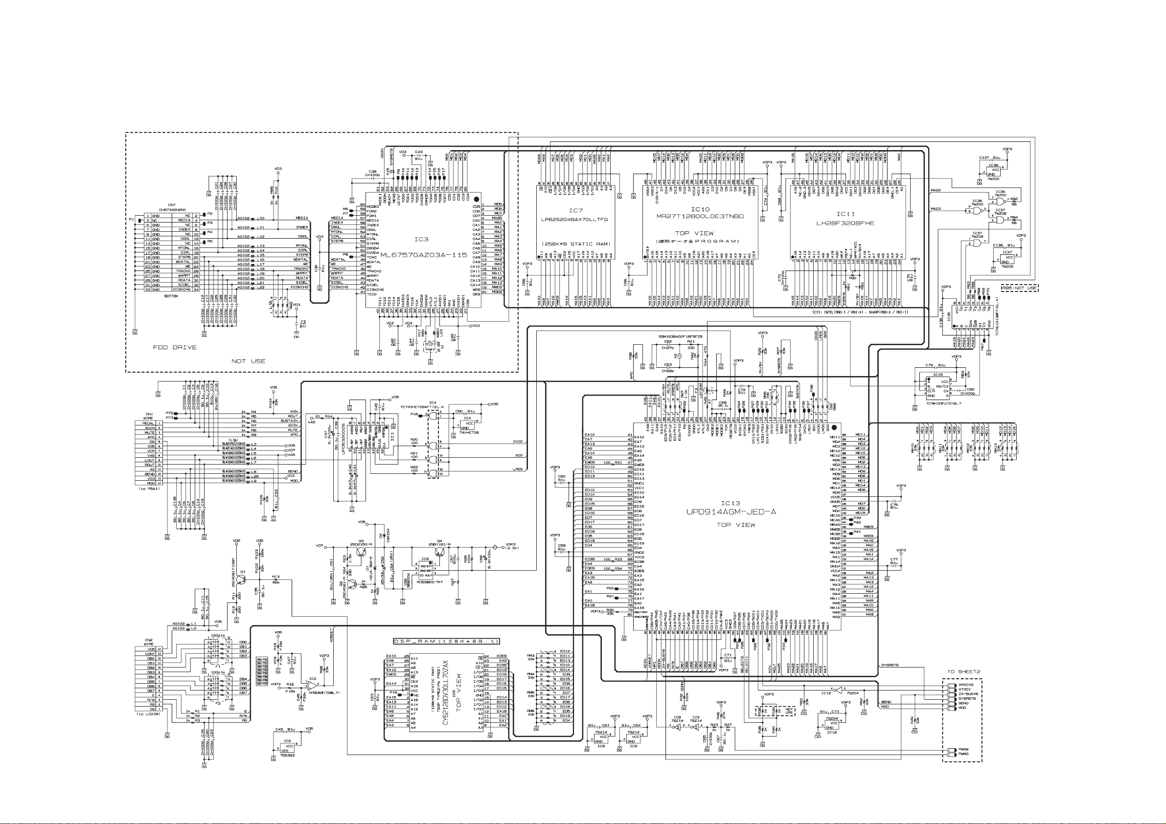
MAIN PCB M740-MDA1 (1/2)
SCHEMATIC DIAGRAMS
— 25 —
Page 28
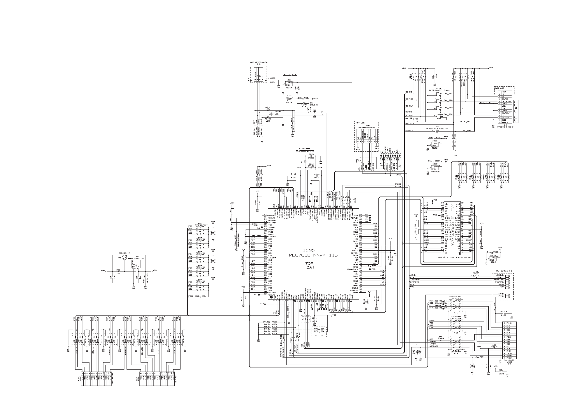
MAIN PCB M740-MDA1 (2/2)
— 26 —
Page 29
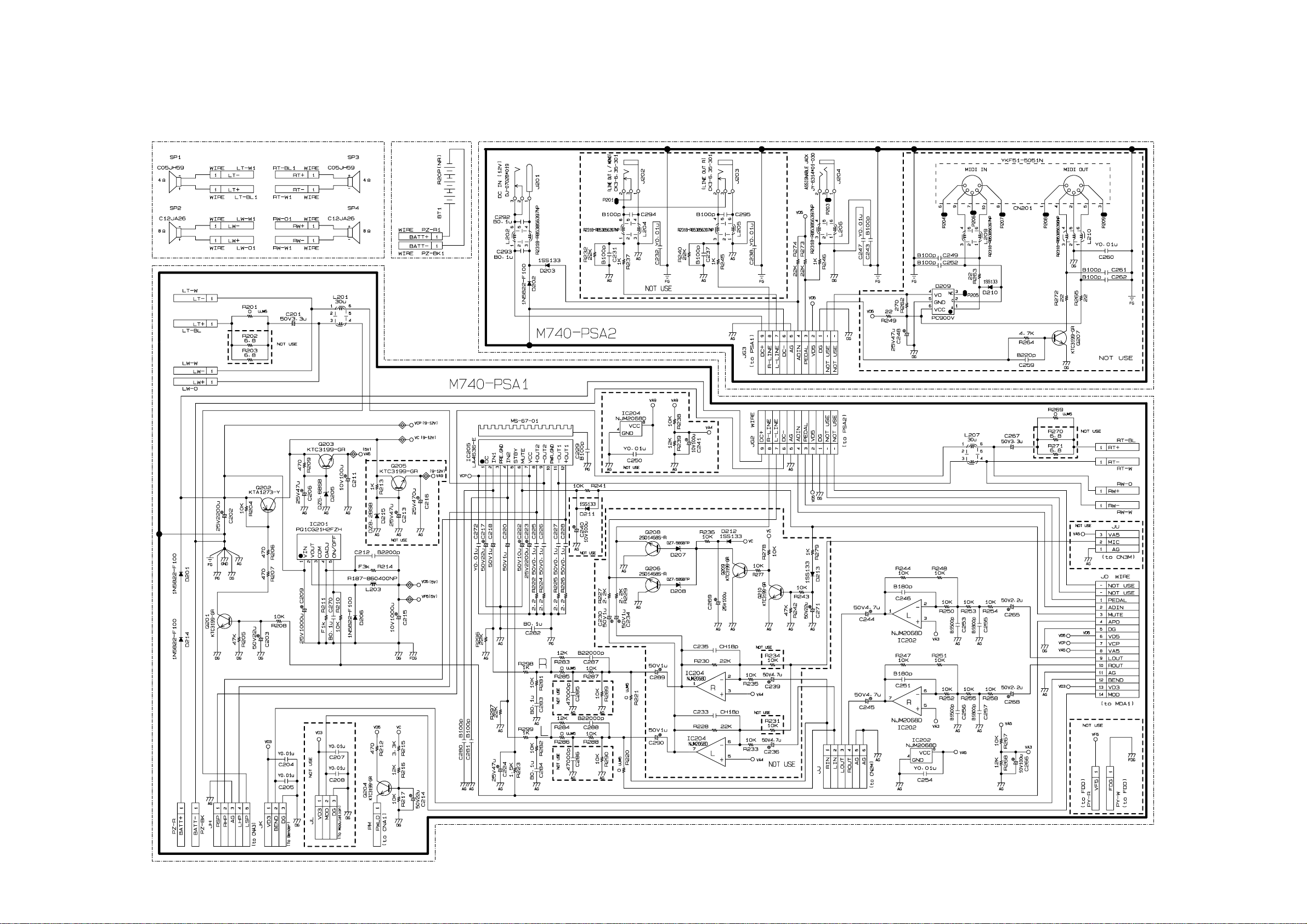
SUB PCBs M740-PSA1/PSA2
— 27 —
Page 30
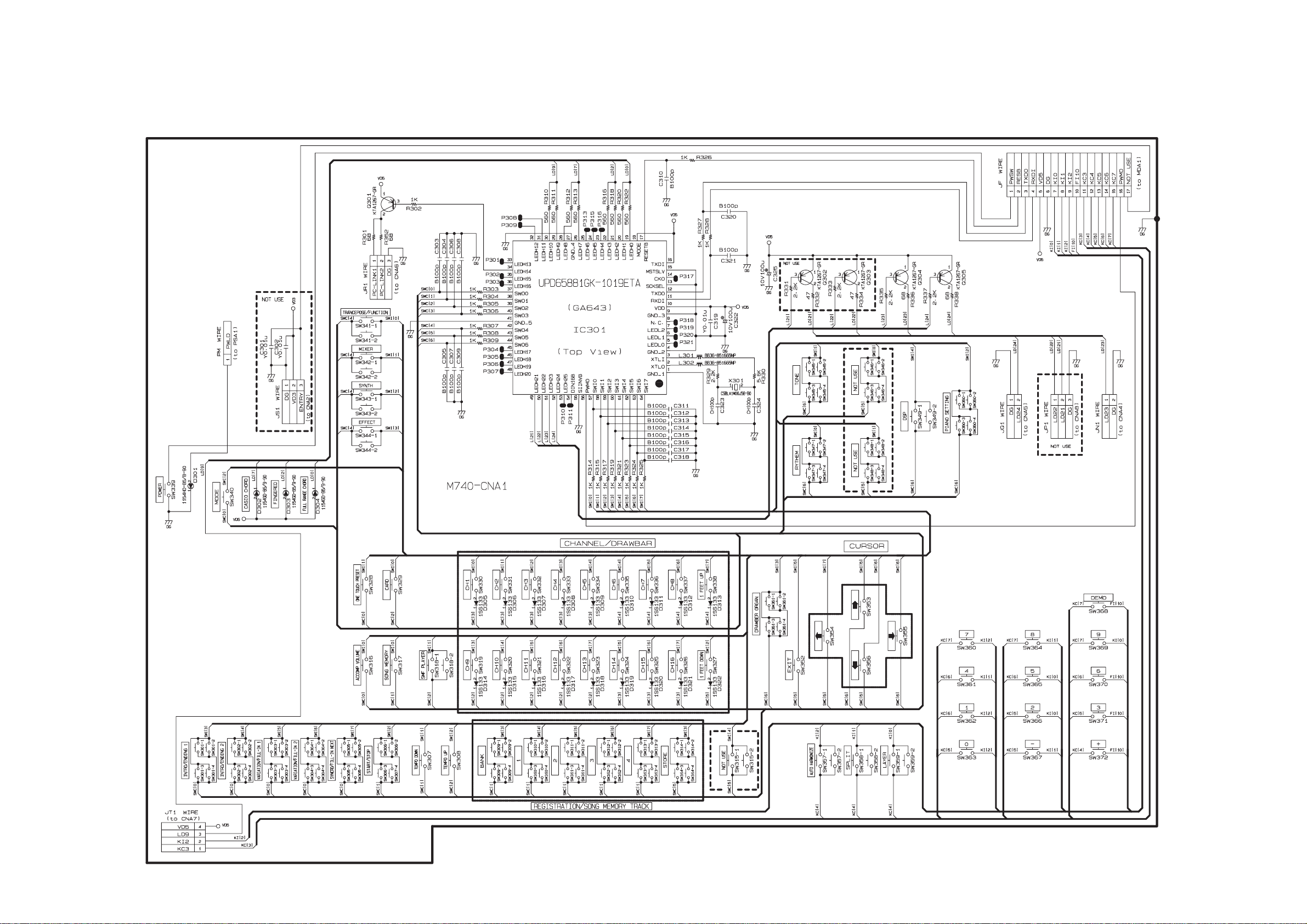
CONSOLE PCB M740-CNA1
— 28 —
Page 31
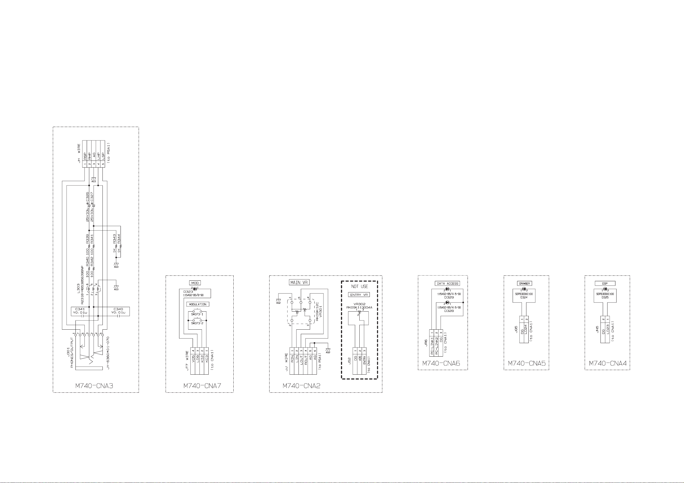
CONSOLE PCBs M740-CNA2/CNA3/CNA4/CNA5/CNA6/CNA7
— 29 —
Page 32
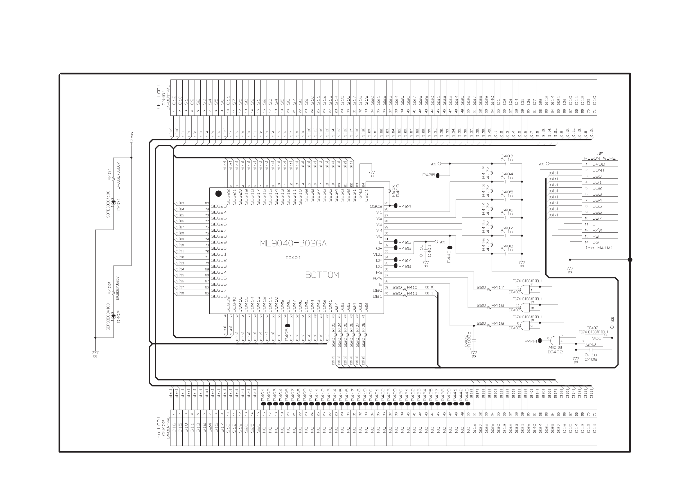
DISPLAY PCB M734-LCD1M
— 30 —
Page 33
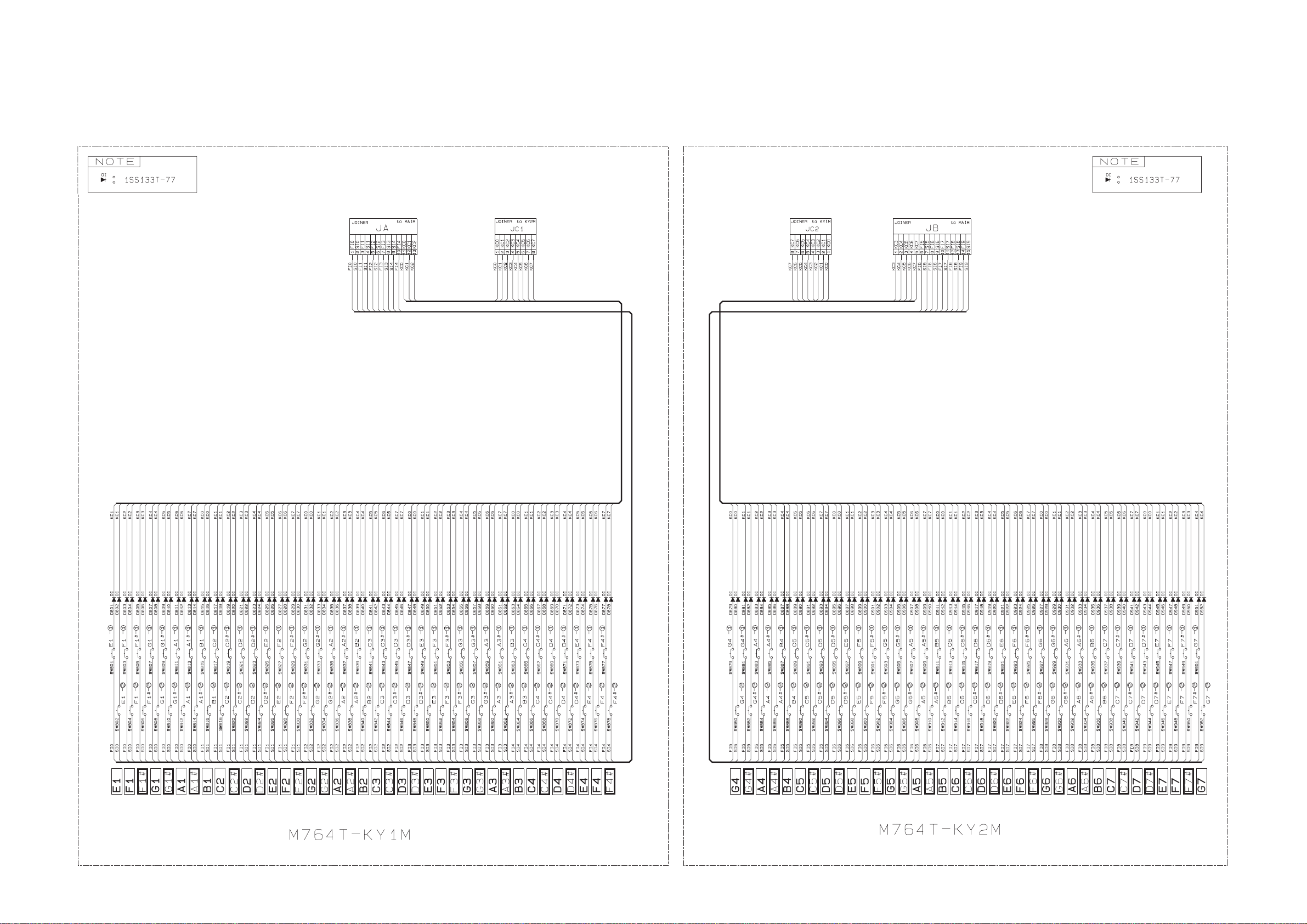
KEYBORD PCBs M764T-KY1M/KY2M
— 31 —
Page 34

CASIO COMPUTER CO.,LTD.
Overseas Service Division
6-2, Hon-machi 1-Chome
Shibuya-ku, Tokyo 151-8543, Japan
 Loading...