

Page 1

SERVICE MANUAL
& PARTS LIST
REF. NO. S/M-813
JUN. 2003
MODULE NO.
QW-2605
BGT-2000
R
(WITHOUT PRICE)
Page 2

CONTENTS
Page
1. SPECIFICATIONS: MODULE QW-2605 .................................................... 1
2. DRAWINGS: MODULE QW-2605
2-1. LCD DIAGRAM ............................................................................................. 2
2-2. CIRCUIT DIAGRAM ...................................................................................... 3
2-3. CHECKING TERMINALS AND COMPONENTS .......................................... 4
3. EXPLODED VIEW: MODULE QW-2605 .................................................... 5
4. PARTS LIST: MODULE QW-2605 ............................................................. 6
5. PRECAUTIONS FOR REPAIR: MODULE QW-2605
5-1. AC (ALL CLEAR) AND REMOVING OF MODULE ......................................7
5-2. ACCURACY CHECKING .............................................................................. 7
6. TROUBLESHOOTING FOR TIME RECEPTION: MODULE QW-2605 ..... 8
Page 3
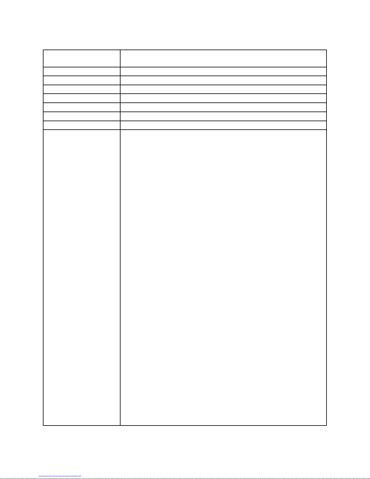
1. SPECIFICATIONS: MODULE QW-2605
Item Detail
Battery CR-1616
Battery life Approx. 2 years
Current consumption 1.24 µA maximum
Alarm system Piezo plate on Cover/Back
Accuracy ±15 sec./month
Accuracy setting system Trimmer capacitor
Accuracy checking See page 7
Functions • Electro-luminescent backlight
Afterglow
• Time calibration signal reception
Auto receive (Three times a day at 2:00AM, 4:00AM and 6:00AM)
Manual receive
Last date/time received display
• ReceivableTime Calibration Signals
Fort Collins, Colorado (Call sign: WWVB, Frequency: 60KHz)
Fukushima, Japan (Call sign: JJY, Frequency: 40KHz)
Fukuoka/Saga, Japan (Call sign: JJY, Frequency: 60KHz)
• Time Recorder
Memory for 50 records, each containing hr, min, sec
• Date Alert
a date alert indicator and the currente date flash for 24 hr after the
aler date arrivers in the Timekeeping Mode
• World Time
29 time zones (28 cities), daylight saving time on/off
• 1/100-sec.stopwatch
Measuring capacity: 23:59'59.99"
Measuring modes: Elapsed time, split time, 1st-2nd place times
• Daily alarms
5 independent daily alarms(4 one-time alarms and 1 snooze alarm)
• Hourly alarms
• Auto-calendar (to year 2039)
• 12/24-hr format
• Regular timekeeping:
hr, min, sec, pm, month, date, day
— 1 —
Page 4
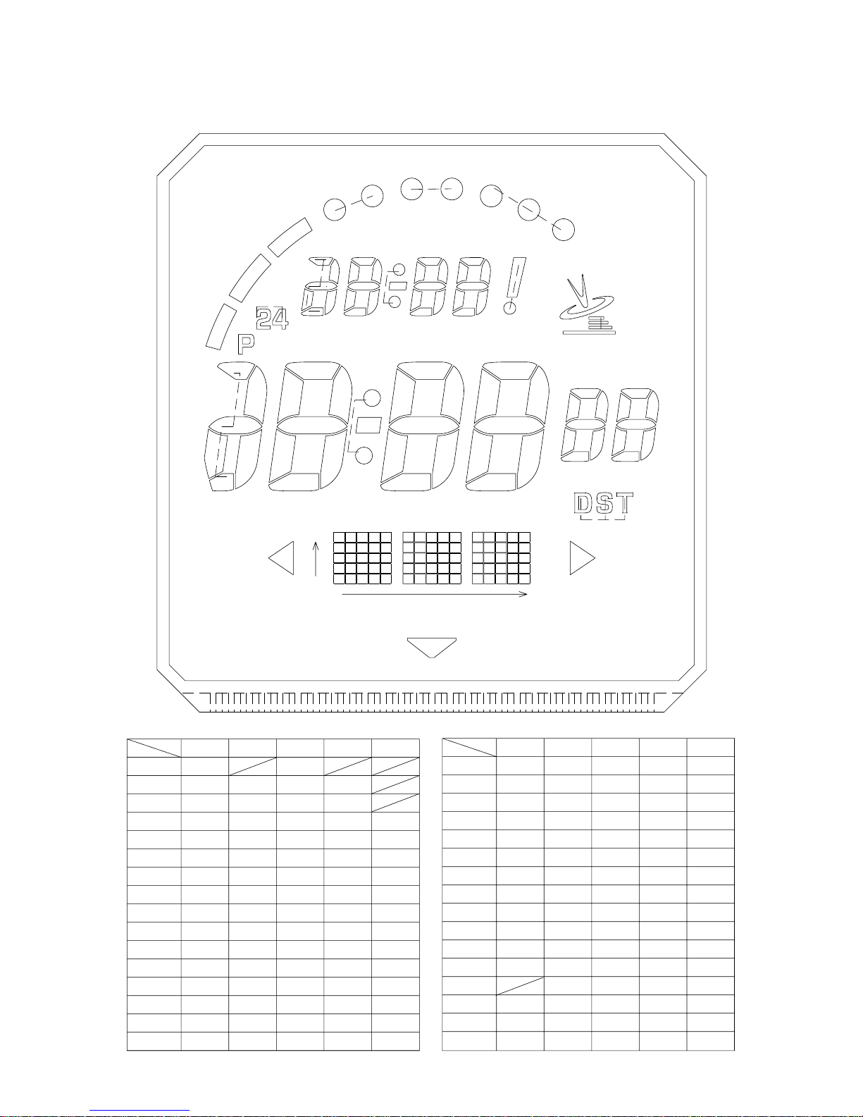
2. DRAWINGS: MODULE QW-2605
2-1. LCD DIAGRAM
alm
ae5
snz
rc1
sig
col1
a8
ae9
24
p
f4
b5
c5
e4
b9
c9
a4
g4
c4
d4
y4
b8
f8
g8
hyp1
c8
e8
d8
col0
b4
f3
hyp0
e3
rc2
rc3
a7
f7
g7
e7
d7
a3
g3
d3
a6
b6
f6
b7
g6
e6
c7
c6
d6
alert
a2
f2
b3
e2
c3
b2
g2
c2
d2
rc3
rc2
rc1
a1
f1
g1
e1
d1
a0
f0
b1
c1
dst
b0
g0
c0
e0
d0
SEG.
L 3
L 4
L 5
L 6
L 7
L 8
L 9
L 10
L 11
L 12
L 13
L 14
L 15
L 16
L 17
L 18
LC5
LC4
LC3
LC2
LC1
COM.
LC1 LC2 LC3 LC4
rc1
rc2
rc3
sig
b6
a6
snz
b7
a7
f7
x14y0
x13y0
x12y0
x11y0
x10y0
x9y0
a0
f0
alert
c6
g6
f6
c7
g7
e7
x14y1
x13y1
x12y1
x11y1
x10y1
x9y1
L27
L26
x14y2
x13y2
x12y2
x11y2
x10y2
x9y2
y0
x0 x14
ok
L34
L33
L32
L31
L30
L29
b0
g0
e0
b1
a1
d6
e6
a2
d7
b3
L28
c0
d0
c1
g1
b2
g2
c3
x14y3
x13y3
x12y3
x11y3
x10y3
x9y3
L25
L24
L23
L22
L21
L20
L19
LC5
SEG.
L 19
L 20
L 21
dst
d1
f1
e1
c2
d2
f2
e2
fwd
x14y4
x13y4
x12y4
x11y4
x10y4
x9y4
L 22
L 23
L 24
L 25
L 26
L 27
L 28
L 29
L 30
L 31
L 32
L 33
L 34
fwdrew
L18
L17
L16
L15
L14
L13
L12
L11
L10L9L8L7L6L5L4
COM.
LC1 LC2 LC3 LC4 LC5
x8y0
x7y0
x6y0
x5y0
x4y0
x3y0
x2y0
ae9
b9
a8
b8
alm
ok
x0y0
x1y0
x8y1
x7y1
x6y1
x5y1
x4y1
x3y1
x2y1
col1
hyp1
rew
x0y1
x1y1
c9
f8
g8
c8
x8y2
x7y2
x6y2
x5y2
x4y2
x3y2
x2y2
p
e8
d8
a4
col0
hyp0
a3
x0y2
x1y2
L3
x8y3
x7y3
x6y3
x5y3
x4y3
x3y3
x2y3
b5
24
f4
g4
b4
f3
g3
x0y3
x1y3
x8y4
x7y4
x6y4
x5y4
x4y4
x3y4
x2y4
ae5
c5
e4
d4
c4
e3
d3
x0y4
x1y4
— 2 —
Page 5

2-2. CIRCUIT DIAGRAM
Rs
Rd
FET
Cc
Rant3
✽8
Rant1
Rant2
16
REG
IN1
1
Creg
15
IN2 PON
2
14
3
AGC
VCC
Cagc
IC
13
FIL1
OUT1
4
Cf13
12
FIL2
OUT2
5
Cf12
Cxt
11
TCO
GND
6
Rpd
10
HOLD
REC
7
9
DEC2
DEC1
8
Rcp
Ccp9
Crl2
Crh3
Crh1
✽1
CSB
✽1✽1
SDO
SCK
✽1
SDI
LC1 - - - LC5
✽1
LCD ( 4.5V 1/3b 1/5d )
L3 - - - - L34
L35 - - - L52
✽1
L1 L2
✽1
T1T2KI1
AC
KI2
S1
Crl3
Crl1
Crh2
KI3
SA
ANT
SB
KI4
✽2✽2✽2
Rxt3
Xtal3
Cbat
Rbat
Short (Soldering) (N trimming)
C5
C4
C3
C2
C1
LL1
Tr1
PZ
Z
BAT
+
C6
✽ 5. Normal Low
✽ 6. LD2 (Normal Low) is used in this module.
✽ 7. LD3 (Normal High) is used in this module.
✽ 4.
✽ 8. Rant1 is not mounted in this module.
GND-KI5: Short (Soldering)
✽ 1. No bonding
✽ 2.
Cel
✽ 3. Latch type key
GND-KI6: Open (No Soldering)
GND-KI7: Short (Soldering)
GND-KI8: Open (No Soldering)
LSI
KC1
KC4
LD3KC3
LD2KC2
✽6
✽7
✽1
TOTAL 93PINS
BONDING 67PINS
Rxt2
Xtal2
VOSC
VCHVDD3 VC1 VC2
VDD1
BD
GND VDD2
✽5
E’
INV
GND
CLF2
L-
LL2
CLF1
VOUT
V+
L+
Xtal
✽1
XT
LD1
✽3
✽4
N1
✽4
✽3✽3✽3
N2
N3
✽4
✽4
N4
XTB
✽3
✽3
✽3
✽3
KI9
KI6
KI7
KI8
KI5
✽2
— 3 —
CT
FRONT
BACK
EL
Page 6

2-3. CHECKING TERMINALS AND COMPONENTS
Transistor
FET
Resistor/Chip
Rd
Resistor/Chip
Cc
Rant2
Resistor/Chip
Creg
Capacitor/Chip
Cagc
Capacitor/Chip
Capacitor/Chip
Cf13
Capacitor/Chip
Tr1
Transistor
Resistor/Chip
Rs
Rant3
6. Oscillator/Crystal
Xtal
(7110 6337)
Resistor/
Chip
LD2KC2
BD
VDD2
S
L
GND
KI1
GND
N4
N3
GND
GND
N2
N1
XTXTB
GND
KI4
2. Tape/Adhesive
(1000 6652)
D
D
DS
S
GND
GND
16
D
2
KI8 KI7
2
GND
1. PCB ASS'Y
(7640 5851)
KI2
Cf12
Rpd
GND
GND
GND
13
12 KI9
14
16
LD3KC3
VDD2
CLF1
CLF2
KI6
KI5
14 13 12
KC1
GND
3GND
GND
3
VOSC
16
GND
KI3
INV
Cel
Capacitor/Chip
C4
IC
Ccp9
GNDGND
KI9
9
VDD2
GND
87
54321
VDD3
VDD1
CLF1CLF2
C5
Inverter
Capacitor/Chip
Resistor/Chip
Detection IC
Capacitor/Chip
Resistor/Chip
Rcp
Capacitor/
Cxt
Chip
9
cp
cp
7
GND
5
VDD2
GNDVCH
GND
GND
GND
L+
VOUT
LGND
VOUT
Capacitor/
C1
Chip
Capacitor/Chip
C2
Capacitor/Chip
XT3
XT2 7
XT2XT3
VOSC
44
GND
AC
VDD2
VOUT
L-L+
VC2 VC1
Rxt3
7
GND
LD3KC3
KI3 KI2
Resistor/Chip
Resistor/Chip
Rxt2
Xtal3
Xtal2
LD2KC2
21S
VC1
C6
C3
Oscillator/Crystal
Oscillator/Crystal
7. Cushion/506
(7211 9631)
Coil
LL1
Varistor
Z
GND
GND
L
L
KI1
L
KI9
VDD2
XT
VDD2
VCH
GND
GND
KI4
3. Capacitor/
CT
Trimmer
(1001 0950)
Capacitor/Chip
Capacitor/Chip
Rbat
Resistor/Chip
Cbat
Top view of P.C.B. ass'y Bottom view of P.C.B. ass'y
Resistor/Chip
— 4 —
LL2
7. Cushion/506
(7211 9631)
Coil
Page 7

3. EXPLODED VIEW: MODULE QW-2605
12 (1009 3594)
5 (1010 0101)
1 (7640 5851)
PCB ass'y
9 (7231 1777)
4 (1010 0100)
16 (7230 1000)
10 (7231 1960)
14 (7207 8852)
8 (7225 1792)
11 (1009 3587)
17 (1005 8538)
13 (7229 0790)
15 (1009 3588)
Battery Lithium
(CR1616)
— 5 —
Page 8

4. PARTS LIST: MODULE QW-2605
-
p
Note: 1. Prices and specifications are subject to change without prior notice.
2. Spare parts are classified as follows according to their importance in after-sales service.
A Rank ---------------------------------------- Very Important
B Rank ---------------------------------------- Important
C Rank ---------------------------------------
3. Batteries in Bulk pack on the tray will be supplied from our Overseas Spare Parts Section under charge basis.
Batteries in Blister pack will be supplied from our Sales Department.
4. As for order/supply of spare parts, refer to the separate publication "GUIDE BOOK for spare parts supply".
Item Code No. Parts Name Specification Applicable Q R
MODULE/WITHOUT MOVEMENT QW-2605YCSA-01 BGT-2000-1/2/9
< The module QW-2605 is "built-in type" which is assembled directly to
the case, therefore the module as the spare parts is not available. >
1 7640 5851 PCB ASS'Y Q255854*1TK QW-2605YCSA Common 1 A
2 1000 6652 TAPE/ADHESIVE Q465964-1 QW-2605YCSA Common 1 C
3 1001 0950 CAPACITOR/TRIMMER CTZ2E-30C-W2-P QW-2605YCSA Common 1 B
4 1010 0100 PLATE/SHIELD Q470819-1 QW-2605YCSA Common 1 C
5 1010 0101 SHEET/INSULATION Q470817-1 QW-2605YCSA Common 1 C
6 7110 6337 OSCILLATOR/CRYSTAL CFS-145OR07 QW-2605YCSA Common 1 B
7 7211 9631 CUSHION/506 Q49364-1 QW-2605YCSA Common 2 C
8 7225 1792 CONTACT/BATTERY(-) Q36151A-1 QW-2605YCSA Common 1 C
9 7231 1777 HOLDER Q456843-1 QW-2605YCSA Common 1 C
10 7231 1960 HOLDER/BATTERY Q254197-1 QW-2605YCSA Common 1 C
11 1009 3587 HOUSING Q152450A-1 QW-2605YCSA Common 1 C
12 1009 3594 INTERCONNECTOR Q470203-1 QW-2605YCSA Common 1 C
13 7229 0790 LABEL/1856 Q461569-1 QW-2605YCSA Common 1 C
14 7207 8852 SCREW Q430508A-1 QW-2605YCSA Common 1 B
15 1009 3588 SUPPORTER/PCB ASS'Y Q152451-1 QW-2605YCSA Common 1 C
16 7230 1000 SPRING/COIL Q458175A-1 QW-2605YCSA Common 1 B
BATTERY/LITHIUM CR1616 QW-2605YCSA Common 1
Less important
BGT-2000L-2B/4B
For the
Notes: Q - Used quantity
rices and minimum order/supply quantities of the above parts, refer to the Parts Price List P.P.L.-595.
R - Rank
— 6 —
Page 9

5. PRECAUTIONS FOR REPAIR: MODULE QW-2605
5-1. AC (ALL CLEAR) AND REMOVING OF MODULE
1. Perform AC (ALL CLEAR) when inserting a new battery, or else the memories and/ or counters may give
erratic displays.
Touch the AC contact and the main plate with the metallic tweezers.
The contact should be made for about two seconds.
2. On removing of the module from the case, please insert the precision screw driver between the module
and the case pointed by arrows.
AC
5-2. ACCURACY CHECKING
Check the accuracy of the module with the quartz timer after switching the module to “ACCURACY
CHECKING MODE”.
The operations are shown below:
A) SWITCHING TO “ACCURACY CHECKING MODE”
While pressing the A button, press B and L buttons at the normal timekeeping mode.
Then all the segments are displayed and the LCD drive signals are changed to the static drive signal
of “32 Hz” so that you can check the accuracy with the quartz timer.
B) CANCELLATION OF THE “ACCURACY CHECKING MODE”
Press any button.
Then the display is returned to its original state.
NOTE: The “ACCURACY CHECKING MODE” will
automatically return to the regular mode
in 1 ~ 2 hour(s) without any operation.
QW-2605
— 7 —
Page 10

6. TROUBLESHOOTING FOR TIME RECEPTION: MODULE QW-2605
START
Check whether the Home City
code is selected correctly.
Perform MANUAL time
calibration signal reception
Signal
reception OK?
No
Perform AUTO time
calibration signal reception
Signal
reception OK?
No
Replace the PCB ass'y
Signal
reception OK?
Yes
OK
Yes
OK
Yes
OK
There is a possibility of the bad location for reception.
No
Replace the Case center
ass'y with antenna
Signal
reception OK?
No
— 8 —
Yes
OK
Page 11

CASIO TECHNO CO.,LTD.
Overseas Service Division
Shibuya-ku, Tokyo 151-8543, Japan
6-2, Hon-machi 1-Chome
 Loading...