

Page 1

EX-Z850
INDEX
FEB. 2006
(without price)
■ Refer to the page 18 after changing the main PCB.
R
Ver.2 : May. 2006
Page 2

CONTENTS
SPECIFICATIONS ....................................................................................................................................... 1
BLOCK DIAGRAM ...................................................................................................................................... 5
TEST MODE ................................................................................................................................................ 6
PROGRAM VERSION UPGRADING .......................................................................................................... 7
1. To update the firmware version ..................................................................................................... 7
2. How to restore the firmware ........................................................................................................... 8
3. To install the firmware .................................................................................................................... 9
ADJ TOOL ................................................................................................................................................. 10
1. Preparation ..................................................................................................................................... 10
2. How to use ADJ Tool when replacing Lens unit ........................................................................ 12
3. How to use ADJ Tool when replacing MAIN PCB ...................................................................... 13
VCOM DC ADJUSTMENT ........................................................................................................................ 14
CURRENT CONSUMPTION ..................................................................................................................... 17
THE COUNTERMEASURE FOR "SYSTEM ERROR" ............................................................................. 17
RESETTING THE PLACE OF DESTINATION .......................................................................................... 18
DISASSEMBLY ......................................................................................................................................... 19
EXPLODED VIEW ..................................................................................................................................... 31
PARTS LIST .............................................................................................................................................. 32
PRINTED CIRCUIT BOARDS ................................................................................................................... 34
SCHEMATIC DIAGRAMS ......................................................................................................................... 36
Page 3
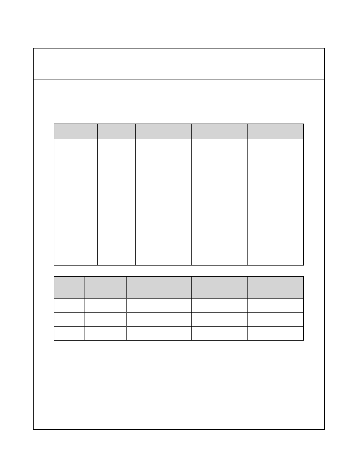
SPECIFICATIONS
Image Files Format Snapshots: JPEG (Exif Ver.2.2); DCF (Design rule for Camera File system) 1.0 standard;
DPOF compliant
Movies: AVI (MPEG-4)
Audio: WAV
Recording Media 8.2MB built-in memory
SD Memory Card
MultimediaCard
Approximate Memory Capacity and File sizes
• Snapshots
File Size
(pixels)
8M
3264 x 2448
8M (3:2)
3264 x 2176
(3:2)
6M
2816 x 2112
4M
2304 x 1728
2M
1600 x 1200
VGA
640 x 480
Quality
Fine
Normal
Economy
Fine
Normal
Economy
Fine
Normal
Economy
Fine
Normal
Economy
Fine
Normal
Economy
Fine
Normal
Economy
Approximate Image
File Size
4.88MB
3.25MB
1.63MB
4.34MB
2.89MB
1.45MB
3.63MB
2.3MB
1.21MB
2.43MB
1.62MB
810KB
1.17MB
780KB
390KB
360KB
240KB
120KB
Built-in memory 8.2MB
1 shot
2 shots
4 shots
1 shot
2 shots
5 shots
2 shots
3 shots
6 shots
3 shots
4 shots
9 shots
6 shots
9 shots
17 shots
21 shots
31 shots
58 shots
SD Memory Card
256MB*
48 shots
72 shots
140 shots
54 shots
81 shots
157 shots
65 shots
101 shots
186 shots
97 shots
143 shots
271 shots
196 shots
286 shots
530 shots
625 shots
938 shots
1742 shots
• Movies
Image Size
(Pixels)
HQ
640 x 480
Normal
640 x 480
LP
320 x 240
* Based on Matsushita Electric Industrial Co., Ltd. products.
Capacity depends on card manufacturer.
* To determine the number of images that can be stored on a memory card of a different capacity, multiply the capacities in the
table by the appropriate value.
Delete Single-file, all files (with protection)
Effective Pixels 8.1 million
Imaging Element 1/1.8-inch square pixel color CCD (Total pixels: 8.32 million)
Lens/Focal Distance
Lenses F2.8 (W) to 5.1(T); f=7.9(W) to 23.7mm (T) (equivalent to approximately 38 (W) to 114mm (T)
Maximum
Recording
Time Per File
Until memory full
Until memory full
Until memory full
for 35mm film)
7 lenses in 5 groups, with aspherical lens
Approximate Data Rate
(Frame Rate)
4.0 megabits per second
(30 frames / second)
2.1 megabits per second
(30 frames / second)
745 kilobits per second
(15 frames / second)
Approximate Recording
Time for Built-in
Memory 8.2MB
16 seconds
32 seconds
1 minute and
29 seconds
Approximate
Recording Time for SD
Memory Card 256MB
8 minutes and
21 seconds
15 minutes and
52 seconds
44 minutes and
17 seconds
— 1 —
Page 4

Zoom 3X optical zoom; 8X digital zoom (24X in combination with optical zoom)
Focusing Contrast Detection Auto Focus
Focus Modes Auto Focus, Macro mode, Pan Focus, Infinity mode, manual focus
AF Area spot, multi, free; AF Assist Light
Approximate Focus Range Auto Focus Snapshots : 40cm to ∞ (1.3´ to ∞)
Macro Snapshots : 10cm to 50cm (3.9˝ to 19.7˝)
Infinity Mode ∞
Manual 10cm to ∞ (3.9˝ to ∞)
• Using optical zoom causes the above ranges to change.
Exposure Control Light Metering :
Exposure: Program AE, Shutter Speed Priority AE, Aperture Priority AE, Manual Exposure
Exposure Compensation : –2EV to +2EV (1/3EV units)
Shutter CCD electronic shutter; mechanical shutter
Snapshot mode
Program AE : 1/2 to 1/1600 second / Manual Exposure / Shutter Speed
Priority AE : 60 to 1/1600 second
Aperture Priority AE : 1 to 1/1600 second
• Above shutter speeds do not apply when using a BEST SHOT scene.
Aperture
White Balance Auto WB, fixed (6 modes), manual switching
Sensitivity Snapshots : Auto, ISO 50, ISO 100, ISO 200, ISO 400
Self-timer 10 seconds, 2 seconds, Triple Self-timer
Built-in Flash
Flash Modes Auto Flash, ON, OFF, High-power Flash, Soft Flash, Red eye reduction
Flash Range Wide Angle Optical Zoom : 0.1 to 4.3 meters (0.33´ to 14.1´)
Recording Functions Snapshot; audio snapshot; macro; self-timer; BEST SHOT; movie with audio (Movie, Short
Audio Recording Time Audio Snapshot : Approximately 30 seconds maximum per image
Monitor Screen 2.5-inch TFT color LCD, 115,200 pixels (480 ✕ 240)
Viewfinder Monitor screen and optical viewfinder
Timekeeping Functions Built-in digital quartz clock
Input/Output Terminals Cradle connector
USB USB 2.0 Hi-Speed compatible
Microphone Monaural
Speaker Monaural
Program AE/Shutter Speed Priority
AE: F2.8 to 8.0*, auto switching* Brightness converted
Manual Exposure/Aperture Priority
AE: F2.8/4.0, auto switching
• Using optical zoom causes the aperture to change.
Movies : Auto
Telephoto Optical Zoom : 0.1 to 2.4 meters (0.33´ to 7.9´)
• Flash Continuous Shutter
Wide Angle Optical Zoom: 0.4 to 3.3 meters (1.3´ to 10.8´)
Telephoto Optical Zoom : 0.4 to 1.8 meters (1.3´ to 5.9´)
* ISO Sensitivity: “Auto”, * Depends on zoom factor.
Movie, Past Movie, MOVIE BEST SHOT) ; voice recording
Snapshot; audio snapshot; macro; self-timer; Continuous shutter (Normal-speed Continuous
Shutter, High-speed Continuous Shutter, Flash Continuous Shutter, Zoom Continuous Shutter,
Multi Continuous Shutter); BEST SHOT; movie with audio (Movie, MOVIE BEST SHOT, Short
Movie, Past Movie) ; voice recording
• Audio recording is monaural.
Voice Recording : Approximately 25 minutes with built-in memory
After Recording : Approximately 30 seconds maximum per image
Date and Time : Recorded with image data
Auto Calendar : To 2049
World Time : City; Date; Time; Summer time; 162 cities in 32 time zones
Multi-pattern, center-weighted, spot by CCD
— 2 —
Page 5
Power Requirements
Power Requirements Rechargeable lithium ion battery
(NP-40) x 1
Approximate Battery Life:
The values below indicate the amount of time under the conditions defined below, until power automatically turns off due to battery
failure. They do not guarantee that you will be able to achieve this level of operation. Low temperatures shorten battery life.
Operation
Number of Shots (CIPA Standard)*
1
(Recording Time)
Number of Shots, Continuous Recording*
(Recording Time)
Continuous Snapshot Playback*
Continuous Movie Recording*
Continuous Voice Recording*
3
4
5
2
Apporoximate Battery Life
440 shots
(220 minutes)
950 shots
(245 minutes)
420 minutes
200 minutes
500 minutes
Supported Battery: NP-40 (Rated Capacitance: 1230mAh)
Storage Medium: SD Memory Card
*1 Number of Shots (CIPA Standard)
• Temperature: 23°C (73°F)
• Monitor Screen: On
• Zoom operation between full wide to full telephoto every 30 seconds, during which two images are recorded, one image
with flash; power turned off and back on every time 10 images are recorded.
*2 Continuous Recording Conditions
• Temperature: 23°C (73°F)
• Monitor screen: On
• Flash: Off
• Image recorded every 15 seconds, alternating full wide-angle and full telephoto zoom
*3 Continuous Snapshot Playback Conditions
• Temperature: 23°C (73°F)
• Scroll one image about every 10 seconds
*4 Approximate time for continuous movie recording, without using zoom.
*5 Voice recording times are based on continuous recording.
Power Consumption 3.7V DC Approximately 3.4W
Dimensions 89(W) ✕ 58.5(H) ✕ 23.7(D) mm
(3.5˝(W) ✕ 2.3˝(H) ✕ 0.93˝(D))
(excluding projections; 19.9mm (0.78˝) at thinnest part)
Weight Approximately 130 g (4.6 oz) (excluding battery and accessories)
Bundled Accessories Rechargeable lithium ion battery (NP-40); USB cradle (CA-31); Special AC adaptor; AC power
cord; USB cable; AV Cable; Strap; CD-ROMs (2); Basic Reference
— 3 —
Page 6

Rechargeable Lithium Ion Battery (NP-40)
Rated Voltage 3.7 V
Rated Capacitance 1230 mAh
Operating Temperature
Range 0°C to 40°C (32°F to 104°F)
Dimensions 38.5(W) x 38.0(H) x 9.3(D) mm (1.5˝(W) x 1.5˝(H) x 0.37˝(D))
Weight Approximately 34 g (1.2 oz)
USB Cradle (CA-31)
Input/Output Terminals Camera connector; USB port; AC adaptor terminal (DC IN 5.3V) / AV output port (Special mini
port, NTSC / PAL)
Power Consumption 5.3V DC Approximately 3.2W
Dimensions 107(W) x 33(H) x 66(D) mm (4.2˝(W) x 1.3˝(H) x 2.6˝(D)) (excluding projections)
Weight Approximately 67 g (2.4 oz)
Special AC Adaptor (Inlet Type) (AD-C52G)
Power Requirement 100 to 240V AC, 50/60Hz, 83 mA
Output 5.3V DC, 650 mA
Dimensions 50(W) x 20(H) x 70(D) mm (2.0˝(W) x 0.8˝(H) x 2.8˝(D)) (excluding projections and cable)
Weight Approximately 90 g (3.2 oz)
Special AC Adaptor (Plug-in Type) (AD-C52J)
Power Requirement 100 to 240V AC, 50/60Hz, 83mA
Output 5.3V DC, 650mA
Dimensions 50(W) x 18(H) x 70(D) mm (2.0˝(W) x 0.7˝(H) x 2.8˝(D)) (excluding projections and cable)
Weight Approximately 90 g (3.2 oz)
Power Supply
• Use only the special NP-40 rechargeable lithium ion battery to power this camera. Use of any other type of battery is not
supported.
• This camera does not have a separate battery for the clock. The date and time settings of the camera are cleared whenever
power is totally cut off (from both the battery and USB cradle). Be sure to reconfigure these settings after power is interrupted.
LCD Panel
• The LCD panel is a product of the latest LCD manufacturing technology that provides a pixel yield of 99.99%. This means that
less than 0.01% of the total pixels are defective (they do not turn on or always remain turned on).
Lens
• You may sometimes notice some distortion in certain types of images, such as a slight bend in lines that should be straight. This
is due to the characteristics of lens, and does not indicate malfunction of the camera.
— 4 —
Page 7
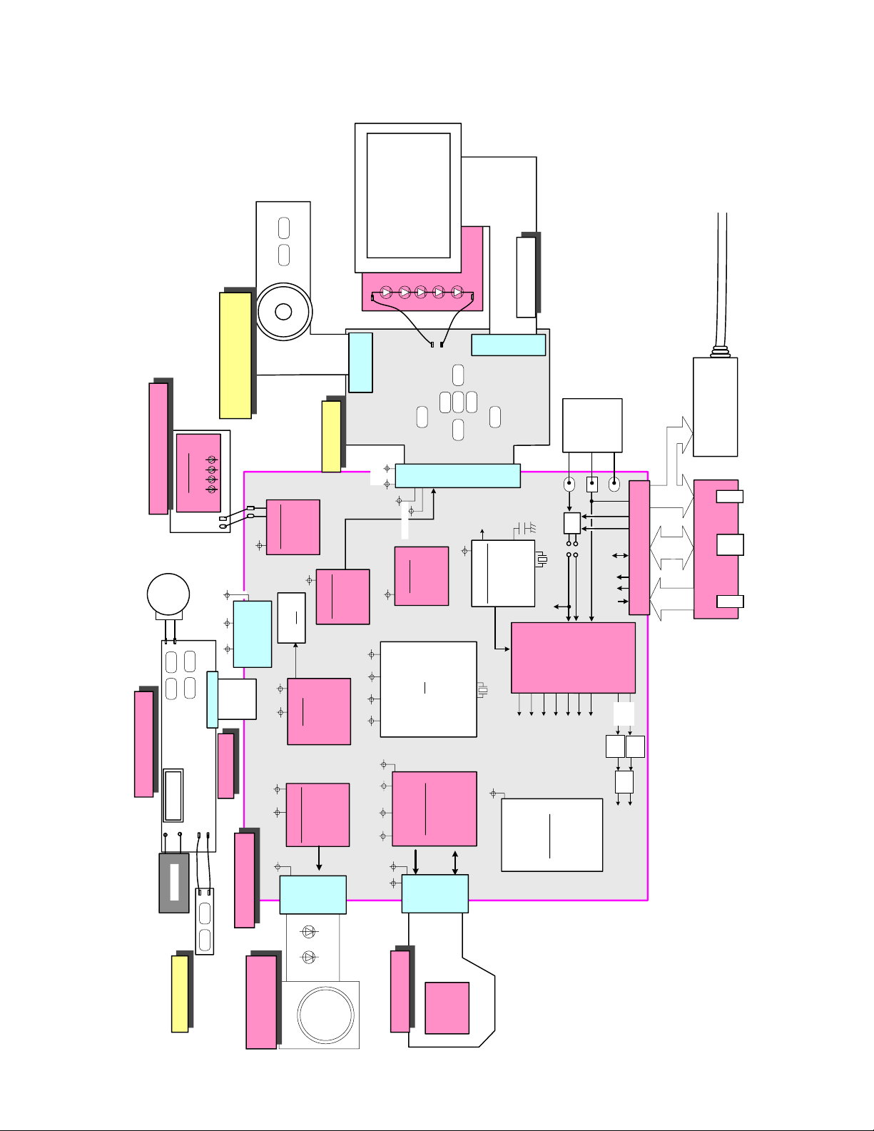
BLOCK DIAGRAM
32.768KHz
F1 F2
8 FPC-KEY2
7 FPC-ST
9 STROBE UNIT
> FPC-LED
4 FPC-KEY1
6 LCD-FPC
5 DIAL SWITCH UNIT
2 MOTOR-FPC
3 FPC-CCD
LENS UNIT
CCD
28 Pin
330V/140uF
SP
DIAL
ZOOM-
ZOOM+
POWER
SHUT
MENU
DISP
UP
OK
PLAYREC
DOWN
RIGHT
LEFT
0.5 mm / 30 Pin
0.5 mm / 29 Pin
0.5 mm / 12 Pin
0.3 mm / 33 Pin
MOTOR DRIVER
VQLP-40 /0.4 mm
5 mm
Voice IC
QFN-24 /0.5 mm
4 mm
SIP
BGA-401 /0.5 mm
SD CARD CN
Battery
LCD / BL
2.5"-LCD
Filter
Vcc12C
VEE6.3C
Vcc15
12V
-6.3V
EVcc3.3
Vcc4.2-3
Vcc4.2-1
Vcc3.3
Vcc3.3
Vcc12C VEE6.3C
Vcc12C VEE6.3C Vcc3.3
VEE1.2 Vcc1.8 Vcc3.0 Vcc3.3
Vcc3.3
BLLEDA/BLLEDC
SW-EVcc3.3
EVcc3.3
Vcc15 Vcc3.3
Vcc3.3
Vcc1.8
Vcc3.3
G-LED
R-LED
Vcc4.2-3 Vcc3.3 Vcc3.3 Vcc3.3A
Vcc1-1
MICBIAS
EVcc3.3 Vcc1-ST Vcc4.2-3
Vcc3.3A
Vcc1.8
Vcc1.2
Vcc1-1
CHGCTL
BATTEMP
CHANGE
DC
GND
D+ / DUSBVcc
USBGND
VIDEO
MONO OUT
AGND
CRDLSW
AC-ADP
USB
AV OUT
DGND
D+ / DVBUS
DC
CHARGE
PWCTL0-5
48MHz
Vcc1-1
VEE7.5
BAT+
+
–
TH
GND1
1 Main-PCB
MIC
0.3 mm / 33 Pin
ST-LED driver
HSON-10 /0.5 mm
3 mm
MOVIE-LED
8pin /3.5 mm
CDS + Vdr + TG
BGA-128 /0.65 mm
9 mm
POWER
SUPPLY
BLOCK
0.3 mm / 33 Pin0.3 mm / 33 Pin
8bit MCU+RTC
BGA-96 /0.5 mm
SW-EVcc3.3
BACKP
Video Amp
SON-10 /0.6 mm
BL-LED driver
SOT-23-6
— 5 —
Page 8

TEST MODE
Note: Never perform the menu items unless otherwise instructed. Doing so may cause destruction
of the data inside, which will make the camera unusable.
■ To boot the test mode
1. While firmly pressing down both [DISP] and [UPPER], turn the power on.
[UPPER] button
2. After the version appears, press buttons in the order of [DOWN], [DOWN], [DISP] and [MENU] in 0.5
second. The diagnostic menu appears.
Ver 1.00
++ KX844 ++
"DOWN" button -> "DOWN" button -> "DISP" button -> "MENU" button
1 :VERSION INFO
2 :USB TCC TEST
3 :ROM UPDATE
4 :LAST MEMORY
5 :FORMAT
"SET" button
"MENU" button
[DOWN] button
1 :USB TCC ON
2 :USB TCC OFF
3 :USB STORAGE
4 :USB SPEED
— 6 —
Page 9

PROGRAM VERSION UPGRADING
1. To update the firmware version
1. Prepare the memory card which contains the firmware for EX-Z850 in the root directory.
EX-Z850.bin
2. Insert the above memory card into the camera, and set a fully charged battery in the camera.
3. Press the [power button] while holding [MENU] depressed. Keep holding [MENU] depressed until
“PROGRAM UPDATE” appears in the display.
• The following appears.
• The version of the firmware in the memory card appears at the bottom of the display.
NOTE 1) When a wrong software is mistakenly used,
PROGRAM UPDATE
YES
NO
NEW VERSION IS
VER 1.00
(As of February 2006)
the message below appears. Update the
firmware again with the correct software.
FILE ERROR!
NOTE 2) When only the version appears in the display
even though you are trying to operate the
camera, charge the battery to the fullest and
try again. The level of the battery indicator
should be highest in order to update the
firmware.
4. Align the white cursor to [YES] by [UPPER] and [DOWN], and then press [SET].
• “NOW LOADING” appears in the display and the update starts.
5. “COMPLETE” appears after the update finishes.
6. Remove the memory card after turning the power off once. Turn the power back on again while holding
[MENU] depressed, and check the version.
• “VER.1.00” appears.
VER 1.00
(As of February 2006)
7. If the version is correct, turn the power off.
8. Finally, check the operation by recording, playing back and deleting an image.
— 7 —
Page 10

2. How to restore the firmware
1. Prepare the firmware restoration program and change its name as follows;
rom844_gm_07.lbn 씮 saturn.bin
NOTE: This software and procedure automatically restores the firmware even if the firmware belongs
to a wrong model code. Make sure to use the correct software for the correct model.
2. Copy the above file to the root directory in the memory card.
3. Insert the memory card into the camera.
4. Set a fully charged battery in the camera.
NOTE: This software and procedure automatically restores the firmware even if the battery capacity of
the camera is low. Make sure to use a fully charged battery to prevent the danger of power
down during firmware restoration.
5. Turn the power on while pressing the [shutter release] button.
If the power does not turn on only by pressing the power button, insert the battery while holding the
[shutter release] button depressed.
• The LED next to the optical viewfinder changes from “green/red blinking”, “green blinking” to “green steady”.
NOTE: This software and procedure automatically restores the firmware even if the firmware belongs
to a wrong model code. Make sure to use the correct software for the correct mode.
6. When the LED becomes “green steady”, the firmware restoration is finished.
Remove the battery and the memory card, and then turn the power off.
7. Turn the power on again while holding [MENU] and [UPPER] depressed.
Check the model name and the program version (PR:) in the opening screen of the test menu.
++KX844++
Ver 1.00
8. If the model name and the program version are correct, perform SYSTEM INITIAL to initialize the
system area.
“MENU + UPPER + PW ON” 씮 “DOWN, DOWN, DISP, MENU” 씮 “3:ROM UPDATE” 씮 “5:SYSTEM
INITIAL”
NOTE: After SYSTEM INITIAL is performed, “SYSTEM ERROR” appears when the power is turned
on again.
9. Write the latest firmware. (Refer to page 6)
After the firmware is written, check the model name and the program version (PR:) in the opening
screen of the test menu.
10. Finally, start the camera normally to check the operation by recording, playing back and deleting an
image. Check also that the colors in the images are not too bright or two dark.
— 8 —
Page 11

3. To install the firmware
Initially, firmware is not installed in the PCB supplied by the parts center.
Install the firmware into the PCB after replacing with a new one as shown in the procedures below.
NOTE: The camera does not operate (only LED becomes “green blinking”) if the firmware is not installed
in the PCB.
<Writing the restoration program 1>
1. Copy the following software to the root directly of the SD card.
Restoration software: rom844_gm_07.lbn
Firmware: EX-Z850.bin
2. Change the name as follows;
“rom844_gm_07.lbn” to “saturn.bin”
3. Insert the SD card into the camera.
4. Insert the battery while holding the [shutter release] button depressed.
The LED next to the optical viewfinder changes from “green/red blinking”, “green blinking” to “green
steady”.
5. When the LED becomes “green steady”, remove the battery and turn the power off.
<System Initialize>
1. Boot the test mode.
2. Press [DOWN] twice and then press [DISP], [MENU].
3. Select “3: ROM UPDATE” and then press [SET].
4. Select “5: SYSTEM INITIALIZE” and then press [SET].
5. When the following message appears, press [SET].
SYSTEM INITIALIZE
START….
PUSH OK KEY?
6. The system initialize is executed. Turn off the power when “SUCCESS” appears.
* “SYSTEM ERROR” appears when the camera is turned off without system initialize.
<Writing the firmware>
1. Turn the power on while holding [MENU] depressed.
2. When “PROGRAM UPDATE” appears, select “YES” and then press [SET].
3. “NOW LOADING” appears while the firmware is updated.
4. When “COMPLETE” appears, the firmware update is complete.
5. Turn the power on and off to check if the camera normally functions. If there is no problem, the firmware
update is successful.
— 9 —
Page 12

ADJ TOOL
■ Introduction
Make sure to perform the adjustment by the USB ADJ Tool “adj03SSAW.exe” when replacing the lens
unit or the PCB.
Here the necessary software, driver and setting are explained to use “adj03SSAW.exe”.
Note that the tool, drivers etc. are available only for Windows.
1. Preparation
1-1. Prepare the necessary software, driver and DLL file.
1) Prepare the following three files.
• Testmode driver
[testmode_driver] folder uusbd.dll
uusbd.inf
uusbd.sys
* [testmode_driver_2.0] is for Windows except Windows98.
* [testmode_driver] is for Windows98 only.
• ADJ tool, USB DLL and ADJ setting file
[adj03SSAW] folder adj03SSAW.exe (ADJ tool itself)
uusbd.dll (USB DLL)
* .adt (ADJ setting file. Sorted by models)
* Place all files in the same folder.
2) Place the testmode driver in an appropriate place.
3) Place all of ADJ tool, USB DLL and ADJ setting file in the same folder.
1-2. Set the camera so that it recognizes the USB test mode.
1) Enter the test menu.
Turn the power on while pressing both [DISP] and [UPPER].
Press [DOWN], [DOWN], [DISP] and [MENU].
2) Move the cursor to “2: USB TCC TEST” and press [SET].
3) Move the cursor to “1: USB TCC ON” and press [SET].
4) The USB test mode flag is now saved in the camera. Turn the power off.
5) When the USB test mode flag is ON, the test menu appears first when the camera power is turned on.
* When turning the USB test mode flag OFF, set “2: USB TCC OFF” in the test menu.
1-3. Install the USB driver for the USB test mode in the computer.
(The following is an example using the Windows Me.)
1) Prepare the USB driver for the USB test mode.
2) Turn the camera power on which is set in the USB test mode as shown in 1-2 and let it enter the USB
test mode directly (the test menu appears right after the power is turned on).
3) Connect the camera in the above status to the computer by the USB cable.
4) The “Add new hardware” wizard appears.
5) Check “Designate the place for the driver (for users with sufficient knowledge)” and press “Next”.
6) Check “Search for the optimum driver for the device (recommended)”.
— 10 —
Page 13

7) Check “Designate the place to search”, designate the place which contains “inf” file in the driver by
pressing “Reference” button, and then press “Next” button.
8) When “Universal USB Driver (VMEM manufacturer’s name)” appears upon message “Searching for
the driver file for the following devices”, press “Next” button.
9) The file copy starts.
(If a message “uusbd.inf cannot be found” appears during the file copy, designate the same place as
in the step 7).
10) Press “Complete” button.
11) Right-click “My computer”, select “property”, and then open “Device manager”.
If “Universal USB Driver (VMEM manufacturer’s name)”,“USB device for UUSBD” can be found, the
computer has successfully recognized the driver.
12) Installing the test driver into either one enables the other one to recognize it.
* How to uninstall the USB driver for the USB test mode
• Connect the camera to the computer while in the USB test mode so that the computer recognizes
the camera.
• Right-click “My computer”, select “Property” and open “Device manager”.
• Select “USB device for UUSBD” , and then “Universal USB Driver (VMEM manufacturer's name)”.
• Press “Delete” button to delete the driver.
• When using Windows98/98SE/Me, delete the following three files;
(NOTE! Do NOT delete “usbd.inf” and “usbd.sys”, whose names are much alike the following.)
C:windows / inf / uusbd.inf
C:windows / inf / other / KashiwanoUUSBD.inf
C:windows / system32 / drivers / uusbd.sys
• The driver has been successfully deleted.
1-4. Use the USB ADJ Tool
1) Prepare ADJ tool, USB DLL and ADJ setting file in the same folder.
2) Turn the camera power on which is set in the USB test mode and let it enter the USB test mode directly
(the test menu appears right after the power is turned on).
3) Boot “adj03SSAW.exe” and use it as follows;
• To read ADJ data from the camera
앶앸 Press “READ ($9)”.
There is no need to set the model by “FW Item Set”.
• To write ADJ data into the camera
앶앸 Press “WRITE ($8)”.
• To save ADJ data which is read
앶앸 Select “File” and “Save All ADJ”, and save it under an appropriate name.
• Open ADJ data which is saved
앶앸 1. Select the model by "FW Item Set", and then press "Load FW ->" button.
2. Select “File” and “Open”, and open the necessary file.
• Language” radio button can switch the language between Japanese and English in which the name
of the ADJ ITEM is displayed.
• “Radix” radio button can switch the data display between decimal and hexadecimal notations.
— 11 —
Page 14

2. How to use ADJ Tool when replacing Lens unit
Make sure to perform the following procedure after replacing the lens.
A floppy disk with the lens data is bundled in the spare parts of the lens unit.
1 Enter the TEST mode.
1. Turn the power on while pressing both "DISP" and "UP" buttons.
2. Press "DOWN" button, "DOWN" button, "DISP" button, and "MENU"
button while the program version is displayed.
3. Select "2.USB TCC TEST", and press "SET" button.
4. Select "1. USB TCC ON", and press "RIGHT" button, "RIGHT" button
and "SET" button.
5. Turn the power OFF.
2 Connect the camera to the computer by the USB cable.
3 Boot "adj03ssaw" .
4 Select the model name and click "Load FW " Key.
• EX-Z850
5 Click "ADJ ALL READ", and display the data on the "adj03ssaw".
6 Find the No.1163, "LCD VCOM DC".
7 Write down this value(data).
8 Replace the Lens unit.
9 Perform the above 1 to 3.
6
0 Select the model name and click "Load FW " Key.
• EX-Z850
A From "File/Open", open the bundled floppy disk, and transfer the data to
the "adj03ssaw".
B Find the No.1163,"LCD VCOM DC"
C Change the data to the former value.(Refer to 7).
D Click "WRITE" button of "ADJ ALL".
E After adjustment, change "1. USB TCC ON" to "2. USB TCC OFF".
4
A
D
— 12 —
Page 15

3. How to use ADJ Tool when replacing MAIN PCB
Firmware is not installed in spare parts.
1 Enter the TEST mode.
1. Turn the power on while pressing both "DISP" and "UP" buttons.
2. Press "DOWN" button, "DOWN" button, "DISP" button and "MENU"
button while the program version is displayed.
3. Select "2.USB TCC TEST", and press "SET" button.
4. Select "1. USB TCC ON", and press "RIGHT" button, "RIGHT" button
and "SET" button.
5. Turn the power OFF.
2 Connect the camera to the PC by the USB cable.
3 Boot "adj03ssaw".
4 Select the model name and click "Load FW " Key.
• EX-Z850
5 Click "ADJ ALL READ", and display the data on the "adj03ssaw".
6 Save the data.
7 Replace the MAIN PCB.
8 Writing the Firmware.
Write the firmware into a spare part after replacing one.
NOTE: If a battery is inserted without the firmware, only LED blinks
green and the camera does not operate.
9 Perform the above 1 to 3.
0 Select the model name and click "Load FW " Key.
• EX-Z850
A Open the file which is saved above, and display the data on the
"adj03ssaw".
B Click "WRITE" button of "ADJ ALL".
C After adjustment, change "1. USB TCC ON" to "2. USB TCC OFF".
6
5
4
A
B
— 13 —
Page 16

VCOM DC ADJUSTMENT
■ Purpose
Readjust the VCOM value to minimize the flicker of the LCD after replacing the LCD or the main PCB.
■ Necessary tools
1. Camera (Charge its battery fully)
2. Photo diode (S2281-01) : See Fig 1.
3. Photo sensor amp (C2719) : See Fig 2.
4. BNC-BNC cable (E2573) x 2 : See Fig 3.
5. 9-volt alkaline battery (6LR61Y) x 2 : See Fig 4.
6. Oscilloscope
■ Preparation
1. The three tools can be obtained from the following global site.
Photo diode (S2281-01)
Photo sensor amp (C2719)
BNC-BNC cable (E2573)
www.hamamatsu.com/
2. 9-volt alkaline battery is a standard one, but can be obtained from the following global site as well.
www.panasonic.co.jp/global/
Fig1 Photo Diode (S2281-01) Fig2 Photo Sensor Amp (C2719)
Fig3 BNC-BNC Cable (E2573) Fig4 6LR61Y
— 14 —
Page 17

■ Procedure
2:LCD
1:ADJ STAT CLR
3:LENS
.
.
.
1:VCOM OK
.
.
.
OK -> Register Write
VCOM = 0xca
This value is an example and differs by products.
Figure (a)
Figure (b)
Figure (c)
Figure (d)
1 :VERSION INFO
2 :VIDEO OUT
3 :USB TCC TEST
4 :TEST MENU
5 :SOUND TEST
6 :IMAGE FLAG
7 :ROM UPDATE
8 :ADJ TEST
9 :REC-INFO
10 :TEST SCRIPT
11 :LAST MEMORY
12 :FORMAT
1. Camera setting
a) Turn the power on while pressing “DISP” and “UPPER”.
After pressing “DOWN” key twice, press “DISP” and “MENU”.
Figure (a) appears.
b) Select “8 : ADJ_TEST” and then press SET.
(See Figure (b).)
c) Next, select “2. LCD” and then press SET.
(See Figure (c).)
2. Connecting the TOOL
d) Pressing SET causes the right figure to appear.
(See Figure (d).)
a) Place two 9-volt alkaline batteries in C2719.
b)
Connect the output terminal of C2719 to the channel terminal of the oscilloscope by the BNC-BNC cable.
c) Connect the input terminal to the Photo Diode by the BNC cable.
d) Turn the oscilloscope and C2719 on.
* Pull the ON/OFF switch of C2719 this way and raise/lower it. (See below Figure.)
— 15 —
Page 18

3. Measurement
a) Connect S2281-01 to the camera’s LCD monitor (see below).
AC Waveforms appear on the monitor screen of the oscilloscope.
* Change the Rf range of C2719 in case the range does not match.
Photo diode
S2281-01
INPUT OUTPUT
Oscilloscope
Photo sensor amp
CAMERA
BNC-BNC cable
LCD
Minimize the
ripple components
b) After AC waveforms of the oscilloscope appear , minimize it by pressing the camera’s up/down buttons
(see the picture).
Make sure to visually check if it has been minimized.
[UPPER] button
After it has been minimized, press SET key.
The screen in the right figure appears and the new VCOM
is written (VCOM adjustment is finished.).
Return to the previous display by pressing MENU or PW key.
[DOWN] button
OK -> Register Write
VCOM = 0xca
ADJ DATA SET!
This value is only an example, and differs by products.
— 16 —
Page 19

CURRENT CONSUMPTION
(1) Current consumption (DC in = 3.80 ± 0.1 [V])
• Make sure that current consumption is less than 240 mA in PLAY mode.
• Make sure that current consumption is less than 330 mA in REC mode.
• Make sure that current consumption is less than 620 µA when power is turned OFF.
(2) The battery indicator changes according to the voltages as follows.
• DC in = less than 3.90 ± 0.02V:
• DC in = less than 3.70 ± 0.02V: (PLAY mode)
• DC in = less than 3.60 ± 0.02V: (PLAY mode)
• DC in = less than 3.40 ± 0.02V: (PLAY mode)
(PLAY mode)
THE COUNTERMEASURE FOR "SYSTEM ERROR"
System error may occur when the battery is removed while data is written to the internal memory.
■ PROCEDURE
1. Initialize the system.
a) Enter the TEST mode.
b) Select "7:ROM UPDATE" and press SET button.
c) Next, select "5:SYSTEM INITIAL" and press SET button.
d) The following message appears.
SYSTEM INITIALIZE
START
PUSH OK KEY?
e) Press SET button and System is initialized.
"SUCCESS !" appears on the monitor.
2. Write firmware.
Refer to the "1. To update the firmware version" on page 7.
Write the firmware.
If the TEST mode boots automatically, change "USB TCC ON" to "USB TCC OFF".
Replace the Main PCB if the camera does not recover.
...
— 17 —
Page 20

RESETTING THE PLACE OF DESTINATION
When the main PCB is replaced, the setting of the destination will be changed, therefore resetting is required.
However, when the firmware is changed or fixed, the setting of the destination will be held, therefore resetting
is not required.
Use the destination setting script to change the destination flag as instructed below.
1. Have an SD card ready that have a corresponding script (autorun.scp) under the root directory.
2. Insert the SD card in the camera and turn on the power.
The script is located at Qv/soft/Adj_soft/exz850/Script in the service CD-ROM.
3. After a few seconds, one of the following messages will be shown in the screen.
The system will change the destination flag and turn off the camera automatically.
For North America
For North America
• Number of menu languages: 10 languages
• eBay scene compatible
Complete
For Europe and UK
For Europe_UK
• Number of menu languages: 10 languages
• Movie filming time limited
Complete
For others
else
• Number of menu languages: 10 languages
Complete
4. Remove the SD card from the camera and turn on the power to confirm if the camera is set as you wish
including the number of the menu languages and the scene of the best shot mode.
If there is no problem, the setting is completed.
— 18 —
Page 21

DISASSEMBLY
* Make sure to use correct screws when assembling since
there are several kinds of them.
It is a good idea to sort them as shown in the right when
disassembling.
1. Remove the battery.
■ Removing the case
2. Remove six screws.
Screws
(S2)
Screws
(S1)
3. Remove the FPC while suspending the rear case assy, and then remove the rear case assy.
Note: Carefully remove the rear case assy as the FPC is connected.
Screws
(S3)
Screws
(S1)
Rear case assy
FPC
— 19 —
Page 22

■ Removing the LCD assy
4. Unsolder four lead wires.
Yellow
Orange
5. Remove the screw.
Black
Red
Screw (S1)
6. Remove the connector, and then the LCD ASSY.
Note: The connector is under the LCD assy.
When removing the FPC, make sure to release the lock of the connector in advance.
Hooks
Assembly Precautions:
Assemble the LCD assy after aligning it with the positioning pins.
Positioning pins
Release the lock of
the connector
Hook
Hooks
— 20 —
Page 23

■ Removing the front case
7. Remove six screws.
Screw (S2)
Screw (S3)
Screws
(S1)
8. Remove the front case assy.
Front case assy
9. Remove three special screws, and then remove the cam ring.
Screw
(S1)
Screws (S5)
Note: Use a special driver as S5 are special screws.
Part code : 9482 9919
— 21 —
Special driver
Page 24

■ Removing the C-FRAME unit
10. Remove one connector.
11. Remove two hooks, and then remove the C-FRAME unit and the FPC.
Connector
Two hooks
Two hooks
12. Remove the FPC .
Note: The condition in which the FPC is removed is the C-FRAME unit.
FPC
Assembly Precautions:
Hook the two hooks.
Let the two lead wires out on the rear case side.
Two lead wires
C-FRAME unit
— 22 —
Two hooks
Page 25

13. Remove two screws.
Remove the tape fixing the lead wires.
Remove two hooks, and then remove the strobe unit and the speaker.
Screw (S6)
Screw (S1)
Tape
13. Remove the speaker.
Note: Speaker is fixed by double-sided tape.
The speaker and the lead wires are not included in the strobe unit.
Tip: Lead wire information
Hooks
Strobe unit
Yellow (Strobe)
Assembly Precautions:
Set the strobe unit after aligning it with the positioning pins.
Fix the lead wires by double-sided tape. Note that the wires should not be stacked.
Positioning pins
Red (Speaker)
Black (Speaker)Blue (Strobe)
Tape
Hooks
— 23 —
Page 26

15. Remove two screws, and then disassemble the C-FRAME unit.
Screws (S5)
Note: Use a special driver as S5 are special screws.
Part code : 9482 9919
Special driver
Zoom lever
Shutter key
Assembly Precautions:
1 Set the zoom lever, shutter key and the shutter coil.
2 Set the zoom lever, shutter
key and the shutter coil which
are already set onto the CFRAME.
Be careful with the direction of
the zoom lever.
Shutter cover
Shutter coil
Zoom coil
3 Set the shutter cover, and then fix it by the special
screws.
— 24 —
Page 27

16. Remove the shutter holder.
Unbend the part in the C-FRAME which is securing the shutter holder.
C-FRAME assy
Shutter holder
Shutter key
Assembly Precautions:
1 While paying attention to the direction of the power key, set it onto the shutter holder.
Shutter holder
Power key
2 Set the shutter holder onto the C-FRAME.
Positioning pins
Hooks
3 Bend the part in the C-FRAME to secure the shutter holder.
Positioning pins
Note: Do not to bend the part in the C-FRAME too much.
It should not go beyond the blue line in the figure.
— 25 —
Attention
Page 28

■ Removing the clamp board.
17. Open the battery cover, and then remove the clamp board.
Hooks
18. Remove two screws, and then remove the strap board.
Screws (S1)
Clamp board
19. Pull out the shaft, and then remove the battery lock.
Assembly Precautions:
Shown below is the detail of the battery lock.
Strap board
Shaft
Battery lock coil
Battery lock
— 26 —
Page 29

■ Removing the key FPC
20. Remove one connector, and then remove the FPC.
Note: The key FPC is fixed by double-sided tape
Connector
■ Removing the Battery case.
21. Remove five screws, and then remove the Battery case.
Screw (S2)
Screw (S4)
Key FPC
Screws (S3)
Assembly Precautions:
Set the battery case after aligning it with the positioning pins.
Positioning pins
— 27 —
Page 30

22. Remove two hooks, and then disassemble the battery case.
Hooks
■ Removing the lens assy
23. Unsolder two lead wires.
Remove two connectors, and then remove the lens assy.
Red
Black
Connector
Connector
24. Remove the screw, and then disassemble the LED unit.
Screws (S2)
Lens assy
— 28 —
Page 31

■ Removing the main PCB.
25. Remove the main PCB.
26. Remove one screw, and then remove the clamp board.
Screw (S6)
■ Removing the battery cover
27. Remove the shaft, and then disassemble the battery cover.
Clamp board
— 29 —
Page 32

■ Assembling the battery panel
1. Extend the sliding part of the battery panel as shown below.
2. Insert the spring.
3. Insert the head of the spring into the battery panel, and then fix it with a pin.
— 30 —
Page 33

2
3
4
1
55
26
24
23
22
21
20
S2
S3
S2
30
33
31
S2
34
35
32
37
36
40
41
42
57
38
29
32
43
44
47
48
S3
S2
S5
39
5
6
10
9
11
19
12
13
14
S1
56
51
49
50
54
52
51
53
7
8
S1
S5
27
28
25
18
16
S4
S1
S1
S1
S1
S3
S2
45
46
S2
15
17
S1
EXPLODED VIEW
— 31 —
Page 34

PARTS LIST
N Item Parts Code Parts Name Specification QTY Price R Remark
Code
N 1 10234663 FRAME ASSY/CENTER TK-RJK508657*001 1 BM C
N 2 10234022 LEVER/ZOOM RJK508558-001V01
N 3 10234009 KEY/SHUTTER RJK508593-001V01
N 4 10234025 COIL/SHUTTER RJK508624-001V01
N 5 10234007 SPEAKER YD-1352
6 10192805 NET/SPEAKER RJK507483-001V01
N 7 10234010 HOLDER/SHUTTER RJK508594-001V01
8 10192808 COIL/ZOOM RJK507424-001V01
9 10192800 COVER/SHUTTER RJK507403-001V01
N 10 10234008 KEY/POWER RJK508592-001V01
N 11 10234936 FPC/STROBE HKW1588-020010
N 12 10234006 STROBE UNIT XEST-K844
13 10192791 CABLE RJK507496-001V01
14 10192792 CABLE RJK507496-002V01
N 15 10234013 CLAMP BOARD RJK508599-001V01
16 10192738 STRAP BOARD RJK507511-001V01
17 10192741 SHAFT/BATTERY RJK507370-001V01
18 10198107 COIL/BATTERY RJK507369-001V02
19 10192768 BATTERY LOCK RJK507409-001V01
N 20 10234670 PCB ASSY/KEY1 TK-RJK508693*001
21 10234019 TAPE RJK508604-001V01
N 22 10234018 FRAME/BATTERY RJK508626-001V01
23 10192755 FRAME/BATTERY RJK507513-001V01
N 24 10233996 BOX/BATTERY RJK508590-001V01
25 10192763 PLATE/BATTERY RJK507375-001V01
26 10153197 SPRING/BATTERY RJK506102-001V01
N 27 10234669 PCB ASSY/MAIN TK-RJK508691*001
N 28 10233998 TAPE/SD RJK508609-001V01
N 29 10233997 RUBBER/MIC RJK508635-001V01
N 30 10234701 LENS UNIT RJK508656*001 TK
N 31 10234002 HOLDER/LED RJK508600-001V01
N 32 10234001 REFLECTOR/LED RJK505664-001V01
N 33 10234700 PCB ASSY/LED TK-RJK508693*003
N 34 10234003 CABLE RJK508613-001V01
N 35 10234004 CABLE RJK508613-002V01
N 36 10233993 CLAMP BOARD RJK508561-001V01
37 10192732 CLAMP BOARD RJK507516-001V01
N 38 10233991 CASE/BOTTOM RJK508589-001V01
39 10192733 SHAFT/DOOR/BATTERY RJK507371-001V01
40 10113040 COIL/BATTERY RJK504304-001V01
41 10220323 PLATE/BATTERY RJK507372-001V02
N 42 10233992 DOOR/BATTERY RJK507408-003V01
N 43 10234016 COVER/FINDER RJK508591-001V01
N 44 10234029 TAPE RJK508603-001V01
N 45 10238066 COVER/LED RJK508824-001V02
N 46 10234030 TAPE RJK507494-007V01
N 47 10234015 PANEL/FRONT RJK508557-001V01
N 48 10234028 CAM RING RJK508537-001V01
N 49 10234667 PANEL ASSY/REAR TK-RJK508655*001
50 10192780 KEY/DIRECT RJK507400-001V01
*1 Floppy disk is bundled.
*2 AC cord is not equipped.
*3 Blade type AC cord is equipped. ( For US )
1
AP C
1
AF C
1
AN C
1
AH C
1
AA X
1
AB X
1
AA C
1
AB X
1
AF C
1
AC C
1
CE C
1
AA X
1
AA X
1
AC X
1
AH C
1
AA C
1
AA C
1
AB C
1
BU C
1
AB C
1
AC X
1
AC X
1
AB C
3
AB X
1
AA C
1
DU A
1
AB C
1
AC C
1
EB A *1
1
AC C
1
AA C
1
BN C
1
AA C
1
AA C BLACK
1
AC X
1
AA X
1
AF C
1
AA C
1
AA C
1
AD C
1
AM C
1
AF C
1
AB C
1
AD C
1
AB C
1
BH C
1
AU C
1
CP C
1
AO C
RED
- 32 -
Page 35

N Item Parts Code Parts Name Specification QTY Price R Remark
Code
N 51 10192783 TAPE RJK507494-001V01
52 10192781 KEY UNIT CA-K842-SE
53 10192795 TAPE/CUR RJK507487-001V01
54 10192779 KEY/SLIDE RJK507399-001V01
N 55 10234666 LCD ASSY TK-RJK508654*001
N 56 10234699 PCB ASSY/KEY2 TK-RJK508693*002
N 57 10235733 LABEL/RATING RJK507519-15
N 57 10235734 LABEL/RATING RJK507519-16
S1 10081372 SCREW RJK502836-001V01
S2 10153233 SCREW RJK506113-001V01
S3 10153183 SCREW RJK502836-003V01
S4 10170510 SCREW RJK502836-004V01
4
AA C
1
AW C
2
AA X
2
AF X
1
DD B
1
AZ C
1
AD X For EU/US
1
AD X
13
AA X
9
AA X
3
AA X
1
AA X
Except EU/US
S5 10170415 SCREW RJK506541-001V01 5 AA X
FU180 10176468 FUSE ERBSD2R50U
N
FU181 10195635 FUSE ERBSD0R75U
N
ACCESSORIES
10193307 CD ROM CK831DCA02R
N 10235735 CD ROM CK844DCA01R
10211064 AV CABLE AV-K835-BK15
10193563 USB CABLE UC-K842-GR10-2
10210351 AC CORD CBL-K835-AC-EU-06
10210360 AC CORD CBL-K835-AC-TW-06
10210354 AC CORD CBL-K835-AC-UK-06
10210350 AC ADAPTOR AD-C52G-WW
10211299 AC ADAPTOR AD-C52J-WW
N 10234034 CRADLE WAU0990-011AE
10193595 BATTERY/LI-ION MK11-2768
10187367 STRAP ST-K872-S
*1 Floppy disk is bundled.
*2 AC cord is not equipped.
*3 Blade type AC cord is equipped. ( For US )
1
AA C
1
AA C
1
AF C
1
AM C
1
AO C
1
AG C
1
AF C Euro type
1
AF C Blade type
1
AR C UK type
1
BC C *2
1
BC C *3
1
CB B
1
BY B
1
AB X
- 33 -
Page 36

MAIN PCB (TOP VIEW)
PRINTED CIRCUIT BOARDS
— 34 —
Page 37

MAIN PCB (BOTTOM VIEW)
— 35 —
Page 38

MAIN PCB (1/2)
SCHEMATIC DIAGRAMS
USB-LED
VBUS
DMINUS
DPLUS
VCC3.3-A
VCC1.2
VCC1.8
VCC3.3
1005
1005
L502
AG700
L500
AG700
VCC1.8
6
C502
1608
B4.7u
6.3V
C500
2012
B22u
6.3V
DGND
AGND
0
0603
R517
SDCLK
SDCMD
PSRSTB
SDDAT1
SDDAT0
USB/SD-BUS
STROBE-BUS
PSCK
PSRDY
PSOUT
PSIN
MT_SCLK
CDTI
VCC3.3D
VCC3.3D
VCC3.3D
VCC3.3-A VCC3.3-A
VCC3.3-A
BLPWM
FLASH_LED_EN
3
MOVIE_LED_EN
3
WATCH
BLCTL
MT_DATA
MT_STB
<
R-LED
<SDRAM I/O>
G-LED
Z_ENC_DET
3
FOCUS0
IRIS3
IRIS2
IRIS1
ZOOM0
IRIS0
CCLK
D-1.2V>
MCKO
<SDRAM I/O>
CSN
LRCK
BICK
1005
SDTO
SDTI
VCC1.2
VCC1.8
VCC1.2
VCC1.8D
VCC1.2
VCC1.8D
2
1uF6.3V
1
C562
1005
VCC1.2A
C565
100pF16V
0603
1
2
DGND
301
302
303
304
305
306
307
308
309
310
311
312
313
314
315
316
317
C558
0.1uF6.3V
318
319
0603
320
321
322
323
ST-CHG-CNT CDRSTB
C560
324
0603
325
0.1uF6.3V
326
327
328
329
330
331
332
333
334
335
0603
R514
336
337
4.7k
338
339
340
341
342
343
344
345
346
347
348
349
350
351
352
353
354
355
356
357
C561
1uF6.3V
358
1
2
359
360
361
362
363
364
365
366
367
368
369
370
371
372
373
374
375
R515
376
0603
377
F5.6k
378
379
380
381
382
383
384
385
386
387
388
389
390
391
392
393
394
395
396
397
398
399
400
401
MOTOR-BUS
293
294
295
296
297
298
299
300
A17
P32/PSCK
P33/PSRST
P51/SD0CLK
P50/SD0CMD
VDD_16
A5/MA3
P34/PSRDY
VSSX_20
P31/PSIN
P30/PSOUT
VSSX_21
P137/RXD2
P135/SCLK1
P136/TXD2
P132/SCLK0
P133/TXD1
P140/SCLK2
P17/TB07
P130/TXD0
P134/RXD1
VCCX1_8
P14/TB04
P15/TB05
P131/RXD0
VCC_7
VSSX_22
P12/TB02
P11/TB01
P16/TB06
VSS_8
VDDQ_7
DSE#
P10/TB00
P13/TB03
VCCX1_9
VSS_SD_15
MRES
SAMRES
P77
VSS_9
VDDQ_8
R/B#
P76
P75
FVCC_2
VSSQ_9
P45/MCLKOUT1
RS#
P44/MCLKOUT0
FVSS_3
VDDQ_9
CS0#
SACE#
P74
VCC_8
VSS_SD_16
P40/LRCLK
P73
P41/BICK
VSS_SD_17
VCC_9
VBUS
DV33
P72
VDD_17
VSS_10
DG33
AV12
P71
VCCX1_10
VCC_10
DM
AG12
P70
P116/MTDCPLS3
VPP
DP
DG12
P111/MTFB0
P115/MTZB0
VDD_18
AG33
DV12
P106/MTFA1
P114/MTZB1
VSSQ_10
REFRIN
AV33
P107/MTFA0
P110/MTFB1
VDDQ_10
WP#
P102/MTIB1
P103/MTIB0
P112/MTZA1
VSS_SD_18
P105/MTIC0
P104/MTIC1
P100/MTIA1
P113/MTZA0
P42/STDI
P43/STDO
P101/MTIA0
P26/TB16
P25/TB15
P23/TB13
DUMMY
VSSX_12P07/INT73P22/TB124P06/INT65P21/TB11
P24/TB147P05/INT58P20/TB109P27/TB1710AUDAT311X27OUT12VSSX_213AUDAT214AUDAT115VDD_116X27IN17TDI18AUDAT019VCCX2_120VSS_SD_121TMS22TRST#23TDO24VSS_126XOUT27TCK28AUDSYNC#29VCCX1_130VSSQ_131XIN32VSSX_333AUDCLK34ASEBRKAK#35VDDQ_136ASEMD0#37P03/INT338P04/INT439VCCX1_240VSSQ_241RTCCLKIN42P01/INT143P02/INT244VSS_245VDDQ_246P00/INT047DQM0/WS0#48WKUP#49VCC_150VSS_SD_251SYSCLK52DQM1/WS1#
1
6
Z_ENC_DET2
283
284
285
286
287
288
289
290
291
292
A18
VDD_15
A2/MA0
A3/MA1
A4/MA2
VSSX_19
VCCX1_7
A12/MA10
VSS_SD_14
P52/SD0DAT0
VCC3.3D
LCD-BUS
8BIT-BUS
R522
C520
6pF50V
1005
1005
DGND
11
6pF50V
4
DSX321G48.000MHZ
3
1005
220
0
R520
1005
VCC4.2-3
VCC1.8
VCC1.2
VCC3.3
VCC3.3-A
EVCC3.3
VCC1-1
VCC15
X520
48M
1
2
C522
DGND
SHUTTER2
VA_STBY
P500
VCC4.2-3
VCC1.8
VCC1.2
VCC3.3
VCC3.3-A
EVCC3.3
VCC1-1
VCC15
DGND
GND3
GND1
GND3
AGND
GND1
AGND
281
282
A15/BA1
P53/SD0DAT1
1
TDI
A16/BA0
VCC1.2D
VCC1.8D
VCC3.3D
VCC3.3A
SDWP
SDCD
SDDAT3
SDDAT2
OFDC
<VCCX1>
5
279
280
VCCX1_6
VSSX_18
<VCCX1>
0603
0.1uF6.3V
C554
267
268
269
270
271
272
273
274
275
276
277
278
DCS0#
DCS1#
SDCS0#
SDCS1#
VCCX1_4
VSSX_17
VCCX1_5
P57/SD0CD
P56/SD0WP
VSS_SD_13
P55/SD0DAT3
P54/SD0DAT2
C
A
B F
305
300
303
25
304
301 203
24
306
23
308
302307
311
309
22
310
314
21
313
312
318
317
316
20
321
19
322
323
18
327
328
17
331
332
333
16
336
337
338
343
15
341
342
346
34815347
14
352
353
13
351
358
12
357
356
361
11
363
362
367
10
366
368
371
9
372
373
378
376
377
8
7
383 385
382
381
6
387
388
386
5
391
392
393
4
395
396
397
6
3
398
399
5
3
2
400
1
1
2
4
B
A
C
IGBTCNT
SHUT_TRG
0603
<SDRAM >
C550
254
255
256
257
258
259
260
261
262
263
264
265
266
RAS#
D
296
297
298
299
315 250
319
324
329
334
339
344
349
354
359
364
369
374
379
384
389
394
10
9
8
7
D
DWE#
CAS#
VDD_14
E
291
292
293
294
295
320
325
330
335
340
345
350
355
360
365
375
380
390
VDD_13
VCCX4_2
VSSX_16
VSS_SD_12
P152/CDSHUT
P151/CDOFDC
P153/CDSHUTM
P154/STLGTSIG0
J
H
276
286
266
282
287
272
267
277
278
268
283
288
289
279
269
284
274
285
275 240
270
280
290
R8J30215AEBGV
370
401
20
15
30
35
24
29
14
19
34
33
13
23
18
28
32
27
12
22
17
31
26 66
16 21
11
F
G
H
E
J
<VCCX4>
0603
0.1uF6.3V
0.1uF6.3V
C548
245
246
247
248
249
250
251
252
253
DCKE
VDD_12
VCCX4_1
VSSX_15
VSS_SD_11
P61/SD1CLK
P60/SD1CMD
P62/SD1DAT0
P63/SD1DAT1
P155/STLGTSIG1
N
L
K
P
M
256
261
251
246
252
262
257
247
263
253
248
258
259
264
249
254
260
255 195
IC500
60
50
55
4025
45
54
49
59
39
44
38
48
53
58
43
57
52
47
37
42
36
51
56
46
41
P
K
N
L
M
244
VSSX_14
241
242
243273
244
245
VCC1.2D
VCC1.8D
VCC3.3D
VCC3.3A
MOTOR-BUS
234
235
236
237
238
239
240
241
242
243
R G
65
64
63
62
61
R
VSS_7
VCC_6
VDD_11
A9/MA7
VSSQ_8
A10/MA8
A11/MA9
A13/MA11
P65/SD1DAT3
P64/SD1DAT2
W
U
Y
V
T
231
221
226
216
236271
227
217
222
237
232
228
223
218
238 211
233
239
234
229
219
224
235
230
225
220
90
70
75
85 5
89
74
69
84
79
73
83
68
88
77
67
72
87
82
81
76
86
71
V
U
W
T
233
Y
232
P66/SD1WP
212
213
214
215
190
185
180326
175
170
135
130
CHG
CENDN
<VCCX5>
V5VCNT
VCCX5_2
228
207281
208
202
198
193
188
183
178
168
163
158
153
148
143
138
133
128
123
118
114
111
10278
101
100
227
P67/SD1CD
AC
173
AC
A14/MA12
0603
C544
225
226
220
221
222
223
224
VDD_10
A6/MA4
VSSX_13
VSS_SD_10
P82/CDPLS2
P81/CDPLS1
P80/CDPLS0
AE
AD
25
205
206
24
204
23
201
200
22
197
196
21
192
191265
20
187
186
182
181
19
176
18
177
17
171
172
166
167
16
161
162
156
14
157
13
151
152
12
147
146
11
141
142
137
10
136
131
132
9
127
8
126
7
121
122
6119
116
117
112
11380
4
110
109
3
107
108
104
106
2
1
103
105
AE
AD
0603
0.1uF6.3V
C546
229
230
231
VSSQ_7
A8/MA6
A7/MA5
AB
AA
209
210
199
194
189
184
179
174
169
164
165
160
159
155
154
150
149
144
145
139
140
134
129
125
124
120
95
115
99
94
93
98
97
92
91
96
AA
AB
CDDAT7
CDDAT6
<VCCX5>
0.1uF6.3V
219
VCCX5_1
218
P83/CDPLS3
MT_RESET
3
217
P84/CDPLS4
216
P85/CDPLS5
CDDAT10
0603
< D-1.2V>
Z_HOME_LED
F_HOME_LED
0.1uF6.3V
C542
213
214
215
209
210
211
212
VCC_5
CDDAT7
CDDAT6
CDDAT10
P87/CDPLS7
P90/CDPLS8
P86/CDPLS6
(top VIEW)
VDD_2
25
R500
100k
VCC1.8
P504
P502
P503
P505
1
1
1
1
TCK
TDO
TMS
TRST
P506
1
ASEBRKAK
4.7k
R502
SHUT_TRG
KINTB
FOUT
P507
1
ASEMD0
WKUPB
AVDET
STBY#54VSSX_455VDD_356DQM3/WS3#57DQM2/WS2#/A158P15659VCCX2_260VSS_SD_361D1562D063P12764VSSX_5
53
PDN
STBYB
VCC3.3
VIDEO
VA_STBY
C590
B1u
VIDEO
HI
VA_STBY
VIDEO OFF
Lo
VDD_466D167D268P9769VCCX2_370VSSQ_371D1372D1473RST#74VSSX_675VDDQ_376D12
65
C595
1005
B1u
IC701
BH76806FVM
L590
1
GLF1608T220M
C1
2
VCC
NVCC
3
VIN
GND
4
STBY
VOUT
1608
1005
C591
C592
B4.7u
B0.1u
0.1uF10V
C504
SDRAM I/O
0
0603
R501
RESETB
1212
8
C2
C594
7
1005
6
5
MODE279VCCX2_480VSSQ_481D1182D483MODE184VSSX_785VDD_686D587D688MODE0
77D378
1005
0.1uF10V
1005
C505
DGND
1uF6.3V
AGND
R592 75
MOTOR-BUS
AUDIO-BUSAUDIO-BUS
LCD-BUS
VCCX2_590VSS_SD_591D992D1093TEST94VSSX_895VCCX2_696D897D798READY#
89
0.1uF10V
1005
C506
D (1.8V)
8BIT-BUS
AV-BUS
VOUT
P510
1
VIDEO
VCC1.2D
VCC1.8D
VCC3.3D
VCC3.3A
USB/SD-BUS
8BIT-BUS
MOTOR-BUS
CCD-BUS
STROBE-BUS
ADCLK
CDDAT4
CDDAT3
CDDAT1
1005
2
1uF6.3V
1
C540
201
202
203
204
205
206
207
208
AVGA
AVCC_2
AVGB
AVSS_2
CDDAT4
CDDAT3
VSSX_12
CDADCLK
CDDAT5
P144/CDDAT1
CDDAT2
AVSS_1
AVOUT
VDD_9
CDDAT9
P145/CDDAT0
AVCC_1
AVOUTB
VSS_SD_9
CDDAT8
P37/ATGPLS0
P36/ADTRG1
AIREF
VCC_4
CDDAT11
P147/CDHD
P35/ADTRG0
AVR
VSS_6
P146/CDEXTCLK
P150/CDVD
AN01
AN00
FVCC_1
VSSX_11
P141/TXD3
AN02
AN03
FVSS_2
VCC_3
P142/RXD3
AN05
AN04
VDDQ_6
VSS_5
P143/SCLK3
AN10
AVREF0
VSS_SD_8
VCCX3_2
LDDAT7
AN11
AN12
VDD_8
VSS_4
LDDAT6
AN13
AVREF1
VSS_SD_7
VCCX3_1
LDDAT4
LDDAT5
PRE
VDDQ_5
FVSS_1
LDDAT3
LDCLK
P126/LDSCLK
VSSQ_6
VCC_2
P121/LDDAT0
P120/LDDAT1
LDDAT2
VDD_7
VSS_3
P124/LDCS
P123/LDVD
P122/LDHD
VSSQ_5
VCCX2_8
P125/LDSTO
D23
D31
VDDQ_4
VSSX_10
VBGP
D22
D30
VSS_SD_6
VCCX2_7
VBB_CNTRL
D21
D29
VCCX1_3
VBGN
D20
D28
DREQ#
D19
D27
D18
D26
D25
VSSX_9
D17
D24
DACK#
CS1#
RSTOUT#
D16
99
100
0.1uF6.3V
0603
C508
D (1.8V)
VCC1.8D
VCC1.2D
MODE:MOVIE
PWM ON Duty
33.3%
PWM_4.345KHz
MODE:FLASH
EN _ High (30msec MAX)
30msec
R508
AGND
1005
1005
F220
6
C538
1
2
200
B1u
199
198
197
196
195
194
193
192
191
190
189
188
187
186
185
184
183
182
181
180
179
178
177
176
175
174
173
172
171
170
169
168
167
166
165
164
163
162
161
160
159
158
157
156
155
154
153
152
151
150
149
148
147
146
145
144
143
142
141
140
139
138
137
136
135
134
133
132
131
130
129
128
127
126
125
124
123
122
121
120
119
118
117
116
115
114
113
112
111
110
109
108
107
106
105
104
103
102
101
CDDAT5
CDDAT2
<SDRAM >
CDDAT9
CDDAT0
0603
C535
B0.1u
CDDAT8
R506
F3.3k
0603
CDDAT11
1
2
1608
C534
B1u
C532
0603
0.1uF6.3V
< D-1.2V>
0603
0.1uF6.3V
3
C517
C530
0603
0.1uF6.3V
<VCCX3>
<SDRAM >
C518
0603
0.1uF6.3V
C516
0603
0.1uF6.3V
<VCCX3>
C514
0603
0.1uF6.3V
<SDRAM I/O>
C512
0603
0.1uF6.3V
D-1.2V>
<
<SDRAM >
C510
0603
0.1uF6.3V
DGND
3
MOVIE_LED_EN
VCC1-1
L172
3.3u
1072AS-3R3M-P3
1005
2012
C174
B10u
0.1uF
C175
10V
GND1
CDSHD
CDSVD
CDSDT
CDSCS
CDSCK
MONOOUT
CCD-BUS
USB/SD-BUS
PW/KEY-BUS
TH
KINTB
KIN2
POWSW
0603
1k
R214
0603
3
61
62
P21/ANI1
P30/INTP1
IC200
67
63
64 53
68
65
69
70
66 43
18
22
21
16
20
15 19
F
E
C203
0603
1005
270
R200
DGND
MOTOR-BUS
ZOOM0_C
ZOOM1_C
ZOOM2_C
ZOOM3_C
IRIS0_C
IRIS1_C
IRIS2_C
IRIS3_C
IGBTCNT
CENDN
PSRDY
59
P0260P03
0.1uF6.3V
ZOOM
ND
SHUTTER
IRIS
HALFSHUT
59
60
6288
26
253
2363113272
0603
C200
KIN1
KIN6
0603
C209
56
P20/ANI057P27/ANI758P24/ANI4
55
57
58
30
29
28
H
1005
1uF6.3V
C204
PAS414HR-VE5R
MT_RESET
POWSW
SHUTSW
1005
55
52
54
45
42
33
K
MT_DATA
MT_SCLK
C208
P130
MT_STB
FOCUS0
54
AVREF
50
51
47
4490
41
39
35
34
L
IRIS3
IRIS2
IRIS1
IRIS0
ZOOM0
KIN4
KIN3
0.1uF6.3V
1uF6.3V
P10/SCK10/TxD0
P16/TOH1/INTP5
49
4876 56
46
40
38
37
36
M24J
P6221P76/KR622P60/SCL0
20
BLCTL
BLPWM
R171
100k
KIN5
P11/SI10/RXD0
P17/TI50/TO50
ZM_ENC2
Z_ENC_DET
ZOOM1_C
ZOOM0_C
ZOOM2_C
IRIS0_C
IRIS3_C
F_HOME_DET
FOCUS0_C
FOCUS1_C
LENS_TH
G-LED
R-LED
1005
SW-EVCC3.3
49
50
P25/ANI551P26/ANI652P22/ANI253P23/ANI3
P13/TXD6
P12/SO10
P15/TOH0
P70/KR0
P32/INTP3
P71/KR1
P73/KR3
P74/KR4
P75/KR5
P72/KR2
P33/TI51/TO50/INTP4
23
24
1005
F20k
R173
C173
KEY-BUS
0603
D10k
R209
C206
0.01uF10V
0603
P2051P2041P208
48
47
46
45
44
43
42
41
40
39
38
37
36
35
34
33
32
31
30
29
28
27
26
25
R432150
R430470
R410
100k
RM202
1005
220
1005
Z_HOME_LED
AUDIO-BUS
1
PSCK
STBYB
0603
R211
PSIN
0
PSOUT
WKUPB
WATCH
0.1uF6.3V
123
45
0.1uF6.3V
C250
C252
0603
678
4
100k
RM211
1
23
RESETB
VCC3.3
1005
P400
GLED
F10k
1
R423
1005
R437
R435
R436
33k1005
33k1005
33k1005
DGND
Q400
RN1903FE
6
1
5
2
4
3
F_HOME_LED
D804
CM830
EZJZ0V120JA
LDDAT0
LDDAT1
LCDCS
LCDDI
LCDSCK
VSYNC
HSYNC
LCDCLK
LDDAT7
LDDAT6
LDDAT5
LDDAT4
LDDAT3
LDDAT2
VCC1-1
L170
NR3015T220M
22u
IC170
1
SHDN
FB
2
OVD
GND
3
VIN
SW
7
TB62752AFUG
2.2uF6.3V
1608
C170
R212
0603
0.01uF
123
0603
R213
1k
1k
0603
33pin
2
4
6
8
10
12
14
16
18
20
22
24
26
28
30
32
34
8
6
5
4
CN400
LDP2_DET
LDP1_DET
ZOOM_TELE
ZOOM_TELE
ZOOM_WIDE
ND_OPEN
IRIS0
IRIS2
FOCUS_DET
FOCUS_LED_DRV
VCC
FOCUS0
FOCUS1
LENS_TH
G_LED
R_LED
FG
046283033001868+
R412
220
R414
1005
220
R416
220
567
C831
4
ND_CLOSE
ZOOM_DET
LENS_TH_GND
1005
1005
4
B0.01u
LDP2_LED_DRV
LDP1_LED_DRV
ZOOM_TELE
ZOOM_WIDE
ZOOM_WIDE
IRIS3
IRIS1
ZOOM_LED_DRV
FOCUS2
FOCUS3
KIN1
4.7k
RM822
123
1005
F22k
0603
R832
D170
MA2Z72000L
R172
F5.1k
1005
BATTEMP
KIN2
1005
PWCTL5
PWCTL4
CHGCTL
PWCTL1
ADPIN
PWCTL2
VCC
VCC
GND
NC
FG
KIN3
678
1005
F22k
R831
12
3
2
1
3
5
7
9
11
13
15
17
19
21
23
25
27
29
31
33
35
R438
1005
KIN6
KIN5
1005
C829
4
6.3V
0603
R822
4.7k
45
4
1005
0603
F22k
F22k
R828 F22k
R829
R830
DGND
C171
R841
C827
1uF
50V
Q200
2SC584600
33k
VCC15
3
1uF
560k
1uF16V
3216
NC_4
AVSS
P53
P52
P50
NC_3
NC_2
P05
P51
P06
P31/INTP2
P77/KR7
1005
F18k
R174
0.1uF10V
1005
GND1
PWCTL0
FOUT
8BIT-BUS
PSRSTB
EVCC3.3
VCC1-1
0603
PAD-C0.8
7015 size
R242
GND1
EVCC3.3
0603
R221
<CRDLSW>
73
0603
74
R227
75
100k
76
C214
0603
0603
0603
R228
F56k
0603
R232
F160k
0603
P200
1
3
0
0603
R240
2
0603
0
DGND
Vc 0.61V
ZM_ENC2
LDP2
10k
1005
R453
10k
R454
1005
0
1005
R911
16
0
16
1005
R408
DGND
VCC1-ST
046283033001868+
1
VDD
3
CHGFB
5
SHUTSW1
7
VBATT
9
VBATT
11
VBATT
13
VBATT
15
POWSW
17
ST-CHARGE
19
SPOUT1
21
SPOUT2
23
GND-1
25
GND-1
27
GND-1
29
DGND
31
DGND
33
KEYZOOM
77
0.1uF6.3V
78
0603
R225
R224 10k
79
100k
80
81
82
C217
83
0.01uF10V
84
C220
85
86
0.1uF6.3V
0603
87
R233
88
0603
100k
89
C225
90
0.1uF6.3V
91
0603
0
C224
0603
R234
92
93
1uF6.3V
1005
0603
94
R236
95
0
C226
96
0.1uF6.3V
0603
C228
0603
6.3V0.1uF
VCC3.3
R904
D360k
R905
D82k
DGND
VCC3.3
VCC4.2-3
31
INV3B
32
INV3
33
C408
VB3
1005
34
VCC
35
0.1uF10V
3
PI
36
SGND
37
VB4
38
INV2B
39
INV2
40
INV1B
9
1005
C411
KEY-1
CN900
2
VDD
4
SHUTSW2
6
KEYEX
8
VBATT
10
VBATT
12
VBATT
14
CRNTCNT
16
ST-TRG
18
DONE
20
EVCC3.3
22
GND-1
24
GND-1
26
GND-1
28
GND-1
30
DGND
32
DGND
33pin
CCD-BUS
VIDEO
C533
0603
0.1uF6.3V
F_HOME_DET
LDDAT7
Z_HOME_DET
LENS_TH
LDDAT6
3
ST_V_LEVEL
LDDAT4
LDDAT5
LDDAT3
LCDCLK
LCDSCK
LDDAT0
LDDAT1
LDDAT2
LCDCS
VSYNC
HSYNC
LCDDI
LCD-BUS
MOTOR-BUS
AV-BUS
MOTOR-BUS
8BIT-BUS
8BIT-BUS
VCC3.3A
VCC3.3A
STROBE-BUS
VCC3.3D
VCC3.3D
VCC3.3D
VCC1.8D
VCC1.8D
VCC1.8D
VCC1.2D
VCC1.2D
VCC1.2D
Z_ENC_DET2
KIN2
SW-EVCC3.3
0603
R226
F160k
C216
B0.01u
0603
R230
F75k
0603
C218
B0.01u
0603
0.01uF10V
0603
C222
11
C240
CH4p
25V
0603
4
3
X200
32.768k
1
0603
C242
SSP-T7-F-20/9
6pF25V
11
VCC3.3
R452
13
1005
22k
OUT
IN+
3
4
VSS
2
VDD
IN-
1
5
NJU7108F3
0.1uF10V
1005
IC401
C450
DGND
1005
16
0
R908
16
0.1uF10V
C407
DGND
MOTOR-BUS
LCD-BUS
SPN
3
FLASH_LED_EN
STROBE-BUS
SPP
AV-BUS
16K-
- 2090 / 10.5K
2530 / 16K
ST_V_LEVEL
CHG
1005
22k
R902
TK11893AM8G0B
1
SW
2
PGND
3
VIN
4
EN
5
EAOUT
D172
3
CRS08
12
IC171
10
VFB
9
GND
8
LED1
7
LED2
6
CONT
P170
P171
AF-SUB,SELF,Movie,FLASH
10uF16V
C176
CONT
MODE LED1 LED2 ILED(mA)
F16k
R177
R176
F10.5k
Low
MOVIE
3216
1608
1608
High
FLASH 10.5K
PWCTL3
SHUTTER2
4
0
100k
0603
R135
RM217
0
1
23
0603
R218
R220
D220k
1608
100k
2.2uF10V
C210
D220k
P120/INTP0
P42
COMP_OUT1
COMP_OUT2
VLC_RTC
IC
PORT_IN
PORT_OUT
AGND
COMP_REF2
COMP_IN1
NC_5
AVDD
COMP_IN2
COMP_REF1
RESET
P40
P122/X2
P121/X1
VDD_MAIN
/VDD_MAIN
VDD_LVI
SUB_OUT2
REGC_RTC
D200
HSD226
IRIS0_C
IRIS1_C
1005
10V
0.1uF
C406
1005
F1.0
R400
27
28
29VC30
RF1
OUT10
IC400
LV8054LP
INV11OUT122RF23OUT114VB25OUT86OUT77PGND2
1005
F1.0
R402
0.1uF10V
IRIS3_C
IRIS2_C
VCC4.2-3
R215
69
72
63
64
65
66
67
P04
P4370P4171IC2
VSS_RTC
P14/RXD6
P00/TI000
P01/TI010/TO00
P141/BUZ/INTP768P140/PCL/INTP6
UPD78F8011F1013E2
71
79
84
8
75G82
780
85
83
72
87
73
81 61
86
77
89
78
5
74
93
92
4
14
10
91
94 17
6
995
2
12 32
3
8
96
5
11
4
1
1
7
A
C
D
B
Top View
NC_12IC13SUB_OUT14SUB_XT15SCL_RTC6SDA_RTC7SUB_XT28VDD_SUB9VDD_RTC10REQ_RTC11EVSS12VSS13REGC14P124/XT215VDD16EVDD17P6318P123/XT119P61/SDA0
1
5
4
6.8k
RM200
1
23
0.1uF6.3V
C202
12
CN200
1pin
PN1
1
8
DGND
FOCUS3_C
FOCUS2_C
FOCUS1_C
FOCUS0_C
0.1uF10V
0.1uF10V
1005
1005
C402
C404
22
23
24
25
26
VB1
OUT121OUT2
OUT3
OUT4
OUT9
20
PGND1
DATA
19
STB
18
SCLK
17
IN62
16
IN61
15
IN52
14
IN51
13
CLK2/PWM
12
CLK1
11
ST
OUT6
OUT5
8
9
10
10uF10V
C400
2012
0.1uF10V
0.1uF10V
C410
C409
ZOOM3_C
ZOOM2_C
ZOOM1_C
ZOOM0_C
R912
0603
10k
Q900
RN1104MFV
3
ST-CHG-CNT
1
2
EVCC3.3
DGND
CCD-BUS
USB/SD-BUS
VBUS
HALFSHUT
SHUTSW
0603
R208
F16k
1
0603
R207
F3.6k
DGND
PW/KEY-BUS
ZOOM3_C
IRIS2_C
IRIS1_C
Z_HOME_DET
FOCUS2_C
FOCUS3_C
VCC3.3
2
EVCC3.3
SW-EVCC3.3
D805
1
1SS400G
220
R840
1005
1608
BLLEDA
BLLEDC
CN600
29pin
1005
CFP5629-0150F
29
BLLEDA
28
BLLEDC
27
SW-EVCC3
26
EVCC3.0
25
KIN1
24
KIN2
23
KIN6
22
KIN5
21
KIN3
20
DGND
19
DGND
18
DGND
17
VDC1
16
VDD
15
LCDDAT0
14
LCDDAT1
13
LCDCS
12
LCDDI
11
LCDSCK
10
VSYNC
9
HSYNC
8
LCDCLK
7
LCDDAT7
6
LCDDAT6
5
LCDDAT5
4
LCDDAT4
3
LCDDAT3
2
LCDDAT2
1
DGND
ILED = 20mA
PWM ON Duty
9%
1608
D15
R170
ILED = 4.0mA
PWM ON Duty
66%
— 36 —
Page 39

MAIN PCB (2/2)
P203
DGND/AGND
P202
DGND/GND2
P201
DGND/GND1
P800
12
DGND/GND3
L6-GNDPAD
DGND
P809
1
CCD-BUS
VCC3.3
P305
GPO41P304
GPO2
CDSVD
VCC12C
VEE6.3C
VCC15
10u
LBMF1608T100M
C144
GND1
VEE6.3
2012
25V 0.1uF
L144
10u
LBMF1608T100M
IC141
NJM2831F12(TE1)
5
VIN
CONT
1
2
C151
3216
GND1
4
GND
3
10uF16V
12
VCC12C
C305
C312
VOUT
2012
NC
C149
25V 1uF
1212
CDDAT0
CDDAT2
CDDAT1
VEE6.3C
CDDAT4
CDDAT3
CDDAT6
CDDAT5
CDDAT8
CDDAT7
CDDAT10
CDDAT9
0.1uF10V
1005
DVDD/VDD
VEE6.3C
V14
V13
V12
V11
V10
CDDAT11
1005
VCC12C
C306
96
97
DVSS
98
NC4
0.1uF6.3V
99
DVDD
100
0603
NC2
101
NC1
102
[LSB]D0
103
NC3
104
D2
105
D1
106
NC6
107
D4
108
D3
109
V14
110
V15
111
D6
112
D5
113
V13
114
V12
115
D8
116
D7
117
NC5
118
V11
119
D10
120
D9
121
VH1
122
V10
123
D12
124
D11
125
VL1
126
DCLK
127
D13[MSB]
128
DRVDD
1608
4.7uF6.3V
0.1uF10V
1
C308
L143
12
AGND
12
GND2
12
GND1
VDD2
DRVSS
V5VCNT
CDRSTB
1005
820
R300
2
D300
1
RB521S30
81
82
83
85
87
88
89
90
91
92
93SD94
V5V
NC9
NC895NC7
NC10
VSS2
36
37
12
34
35
11
31
32
10
27
28
9
23
24
8
19
7
20
15
16
6
5
12
7
8
4
5
4
3
2
3
2
111
1
128
B
A
CP3P3
CPVSS
CP1P88CPCLI
CPFCT4CPFCB
VM1
2
3
6
7
5
NC11
LDOVSS
38
40
39
41
42
33
30
29
26
25
22
21
18
17
13
14
9
10
6
125
124
128
126
123
C
D
V910V811SENSE12LDOIN13V714V6
9
LDO1P8EN86LDO3P2EN
VCC
NC1284RSTB
47
43
48
44
45
49
46
50
IC300
AD9927
118
122
117
121
116
120
115
119
E
LDOOUT
15
16H117V418
VSS1
F
GND3DGND
PAD
GND2
C310
0.22uF16V
1608
V8
V9V6V7V5V4
CDSHDH1
1
VD
73HD74
75
76VD77
78
VDD179NC1380SYNC
GPO1
XVVDD
XSUBCNT
51
55
59
63
60
52
56
64
61104
65
53
57
54
58
62105
74
77
78
81
82
85
86
89
90
93
94
110
114
97
109
113
106
108
112
103
102
107
111
J
H
K
G
H2
HVSS121V3B
HVDD1
V5
V3A
20
22
24
19
23
1005
0.1uF10V
C304
V3B
V3A
CDSCK
P303HDP302
0.1uF6.3V
0603
C316
IOVDD/XVVDD
VEE6.3C
65
66
67
70
71
72
H3
25
SCK
GPO3
GPO668GPO869GPO4
GPO2
IOVDD
IOVSS
68
66
69
67
70
71
73
72
75
76
79
80
83
84
87
88
91
92
95
96
98
99
101
100
L
M
V2A
V2B27H428H5
26
V2A
V2B
H2
64
GPO7
63
SDATA
62
DECEN
61
GPO5
60
SL
59
REFB
58
LM
57
BGSWEN
56
AVSS
55
REFT
54
OPOUT
53
CLI
52
AVDD
51
CCDIN
50
OPIN
49
CLO
48
TCVDD
47
TCVSS
46
VMM
45
VLL
44
CLIVDD
43
RG
42
SUBCK
41
RGVSS
40
RGVDD
39
VH2
38
HL
37
VL2
36
H8
35
H7
34
HVDD2
33
VM2
V1A30V1B
HVSS2
29
31H632
VCC12C
V1A
V1B
VCC1.8
SUBCK
V1A
V1B
V2B
V6
V10
V13
V3A
V5
CCDIN
VEE6.3C
VCC12C
D330
12
1SS400T1
C330
1uF25V
1608
8
L304
L302
1005
L300
1005
AG700
2012
C314
6.3V 10uF
C320
0.1uF10V
1005
C328
0.1uF10V
1005
1005
AG700
AG700
1
P306
GPO7
CDSDT
CDSCS
C319
0603
0.1uF6.3V
1uF6.3V
1005
C315
C317
0603
0.1uF6.3V
ADCLK
C318
R332
R331
1.8k
27k
0603
0603
C334
1005
1uF6.3V
CCDIN
16V 0.1uF
1005
8
RG
SUBCK
HL
RG
H2
OFDC
C350
2012
12
D333
GND2
10V 10uF
7
D333
C300
10uF6.3V
1608
R320
R321
1SS400T1
3
R330
V-Driver
820
820
1005
100k
C332
0.1uF25V
1608
4
15
32
30
28
26
0603
24
0603
22
20
18
16
14
12
10
8
6
4
2
VCC3.3
D331
12
AUDIO-BUS
1SS400T1
VSUB
33pin
CN300
V5C
V5A
V3C
V3A
V3L
V5L
V1C
V1A
GND
VOUT
PT
GND
RG
GND
H2
SUBSW
046283033001868+
2
33
V6
31
V5B
29
V4
27
V3B
25
V3R
23
V5R
21
V2
19
V1B
17
V1S
15
GND
13
GND
11
VDD
9
GND
7
HL
5
H1
3
GND
1
VSUB
1,2
CCD (33PIN)
SPN
SPP
MCKO
MONOOUT
C704
6.3V 10uF
C702
VCC12C
V14
V4
V11
V2A
820
V9
R322
0603
V12
R323
0603
8
820
V8
V3B
8
V7
R324
0603
2.7k
HL
2012
H1
C341
16V 4.7uF
VSUB
VCC3.3-A
L701
1005
AG700
22uF6.3V
0.1uF6.3V
C708
C706
0603
2012
GND3
BICK
LRCK
SDTI
SDTO
CDTI
12
BICK
AK4633VN
SVSS
19
11
20
0603
FCK
IC702
SVDD21AOUT
C712
R704
10
SDTO
22
1uF6.3V
220
CCLK
7
CCLK8CDTI9SDTI
BEEP23MPI24MIC
1005
VCC3.3
10
R700
1005
2012
0603
0.1uF6.3V
DVDD
13
DVSS
14
MCKI
15
MCKO
16
SPP
17
SPN
18
0603
R706
20k
VCOC
AVDD
AVSS
VCOM
C716
CSN
PDN
1uF6.3V
6
5
4
3
2
1
1005
3
GND_2
4
POWER
SPM0102ND3
IC703
PDN
CSN
10
R708
0603
R710
C726
B4700p
10k
0603
C722
C724
1608
0603
B2.2u
0.1uF6.3V
C720
0603
2012
C718
6.3V 10uF
0.1uF6.3V
0.33uF6.3V
10
14
C728
16
17
1005
R714
R713
0
0
1005
1005
2
GND_1
10
14
1005 68
1
R712
OUTPUT
10
14
16 17
PW/KEY-BUS
VCC4.2-3
VCC1.8
VCC1.2
VCC3.3
VCC3.3-A
EVCC3.3
VCC1-1
VCC15
AGND
GND3
DGND
GND1
TH
BATTEMP
KIN4
CHGCTL
AV-BUS
R809
4.7k
4
ADPTIN PullUp
RN1104MFV
EVCC3.3
1005
R251
1005
0.01uF25V
C803
DGND
ADPIN
3
Q180
2
DGND
F22k
1005
AGND
AG700
AG700
L592
L702
VOUT
MONOOUT
Q800
DGND
6
RN4985EF
1
AVDET
1
5
2
USB-LED
DC
R181
R182
VCC4.2-3
DPLUS
DMINUS
CUS01
12
D180
10
1005
1005
1k
PAD
P180 BAT+
P181 TH
P182 BAT-
Q181
4
5
6
SSM6J51TU(TE85L.F)
FU180
2.5A
ERBSD2R50U
3
2
1
GND1
4
4
LSI _
D801
D802
EZJZ0V270RA
EZJZ0V270RA
3
L811
41
23
NTM1210-SC900
GND1
DC
D803
EDZTE5.6B
R804
21
270
1608
DGND
EZJZ0V270RA
D806
VBUS
CN800
1
USBGND
2
D+
3
D-
4
USBGND
5
USBGND
6
VOUT
7
USBLED
8
BATTEMP
9
CRDLSW
10
CHGCTL
11
NC
12
AGND
13
MONOOUT
14
AVDET
15
NC
16
GND1
17
GND1
18
GND1
19
GND1
20
DC
21
DC
22
CHARGE
23
CHARGE
24
CHARGE
25
CHARGE
26
USBVCC
27
USBGND
28
USBGND
29
USBGND
30
USBGND
4
OPEN PAD
SDDAT3
SDCMD
SDCLK
SDDAT0
SDDAT1
SDDAT2
SDCD
SDWP
R801
P807
VCC1-ST
VCC1-1
VCC3.3
1005
L800
BD102
123
45
1005
10k
RM803
4
1005
L810
HW680
1
1
WRITE PROTECT
SDDET
P802
P801
SD-PCB
678
1005
47k
47k
R805
C802
0.1uF10V
1005
2012
C801
B10u
DGND
CN802
SCDA3A0600
1
DAT3
2
CMD
3
VSS
4
VSS
5
VDD
6
VDD
7
CLK
8
VSS
9
DAT0
10
DAT1
11
DAT2
CARD DETECT
12
13
VSS
WRITE PROTECT
14
15
VSS
PWCTL1
PWCTL0
PWCTL4
SD-CONNECTOR
PAD-C0.8
VCC1-1
2012
GND1
PWCTL3
P130
PAD-C0.8
L130
6.8u
C4-K1.8L-6R8
1
2
3
CE
VDD
VOUT
SOT25
GND
EXT
2012
4
C130 B10u
5
C131 B10u
IC130 4.2V
XC6367A425MR
D130
CUS01
12
Q130
1
2012
C132 B10u
6
2
5
3
C133
4
SI1406DH-T1
IC100
XC9225A12CDR
P101
CE/MODE
VOUT
L100
IC110
1.2V
USP-6B
1.8V
3
VSS1
4.7u
2
LX
1
1069BS-4R7N-P3
2012
C101
P110
3
2
1
L110
12u
1069BS-120M-P3
PAD-C0.8
2012
C112
1
VOUT
VSS1
LX
SON
VCC1.2
P100
VCC1.2
B22u
VCC1.8
330
R111
B10u
2
Q110
DTA123JM
3
GND1
2012
GND1
C111
4
VSS2
5
VIN
6
C100
B10u
XC9225A186DR
CE/MODE
4
VSS2
5
VIN
6
2012
B10u
GND1
1005
R141
47k
L140
12u
1069BS-120M-P3
Q140
8
12
D140
7
RB551V-30
6
D141
RB551V-30
12
1005
1005
L141
7
A997AS-6R8M-P3
-7.5V : R145 75K R155 0 R140 15K
-6.3V : R145 62K R155 1K R140 15K
R142
D2k
1005
D2k
1005
1005
D56k
R144
R143
321625V
D62k
10k
1005
R145
R146
1005
D1k
R155
CH56p
C145
Q141
SI1013R
23
0603
R149
470k
1
321625V
1M
0603
C150 B10u
R150
C146 B10u
3
201210V
2
C147 B10u
C141
Q142
RN1104MFV
25V 0.022uF
VCC15
1005
11
13
VEE6.3
1
GND1
FU181
0.75A
ERBSD0R75U
PWCTL1
4
5
GND
DTC1
VFB1
IC140
VREFOUT
VIN
VFB26DTC2
7
8
1005
R140
D15k
1005
C140
B0.33u
C142
B0.33u
C148 B1u
1005
1005
2012
1
2CE3
EXT1
EXT2
9
10
C143 B10u
R1280D002B
1
2
3
45
SI5513DC-T1-E3
GND1
100uF10V
F951A107MBAAQ2
P140
PAD-C0.8
PWCTL2
1
Q131
RN1104MFV
R130
2
3
1005
100k
R132
1M
1005
Q132
3
4
2
5
1
6
SSM6J51TU(TE85L.F)
VCC4.2-3
GND1
PWCTL5
VCC4.2-1
IC190
GND1
IC120
XC9225A33CMR
VIN
VSS
CE/MODE
3.3V
Step Down
C190
S-1323B33NB-N8STFG
3
4
B1u
5
LX
4
VOUT
ON/OFF
VIN
7
L120
A997AS-100M-P3
1005
C136
B0.022u
P131
PAD-C0.8
1
2
10uF6.3V
C120
3
2012
3.3V
VOUT
P190
PAD-C0.8
2
VSS
1
EVCC3.3
C191
B2.2u
VCC3.3
20
R121
2
C121
B22u
2012
10
3
Q120
DTA123JM
1608
1
180
R122
IC160 3.3V
S-1132B33-I6T2G
1uF6.3V
1608
C160
ON/OFF4NC
5
VSS_2
6
VIN
Regulator
3
2
VSS_1
1
VOUT
P160
PAD-C0.8
VCC3.3-A
2.2uF6.3V
1608
C161
GND1
— 37 —
Page 40

Ver.1 : Mar. 2006
• The program for EX-Z850 has been changed. (P8, P9)
• RESETTING THE PLACE OF DESTINATION is added. (P18)
Ver.2 : May. 2006
Correction of the RESETTING THE PLACE OF DESTINATION (P18)
CASIO COMPUTER CO.,LTD.
Overseas Service Division
6-2, Hon-machi 1-Chome
Shibuya-ku, Tokyo 151-8543, Japan
 Loading...