

Page 1
SERVICE MANUAL
(without price)
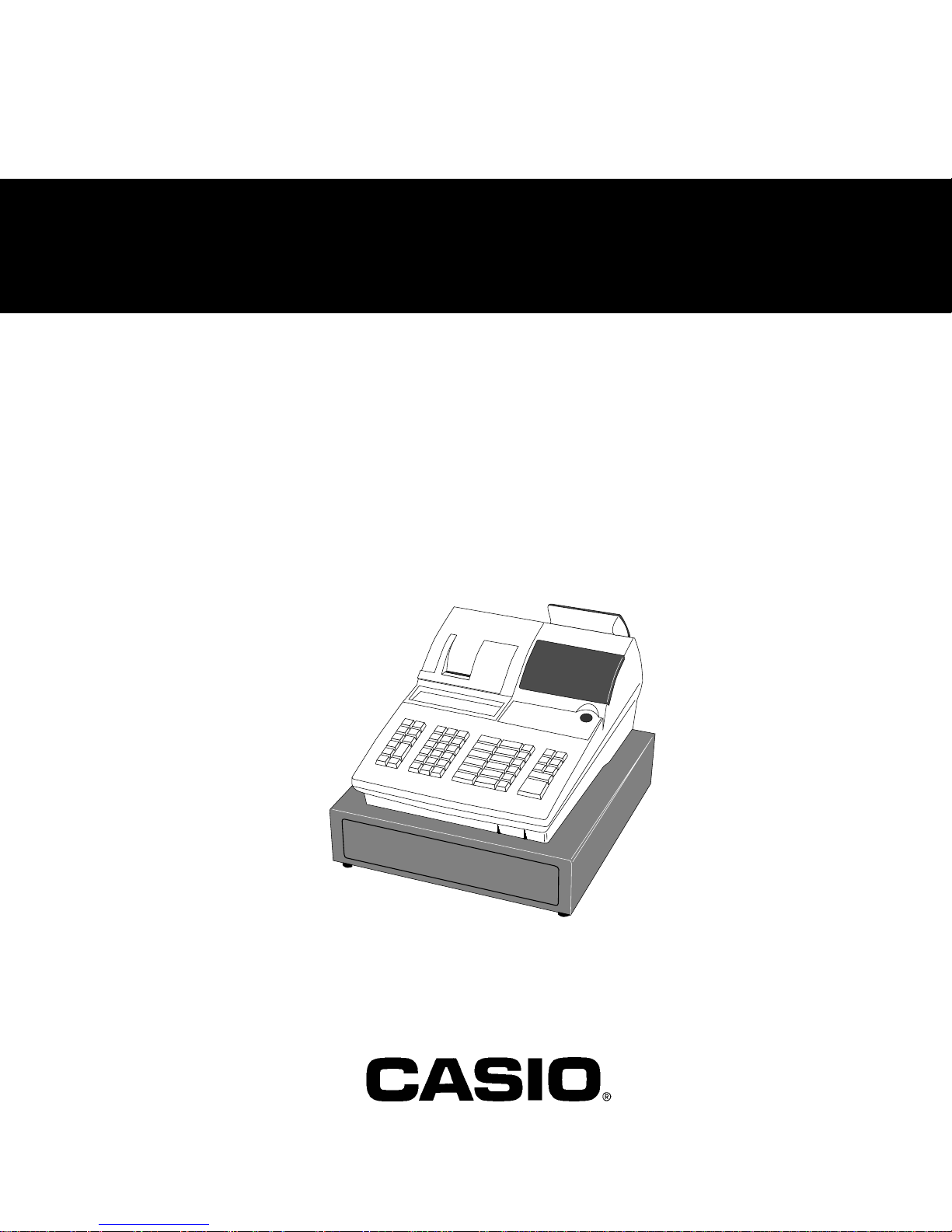
ELECTRONIC CASH REGISTER
CE-6000 (EX-475A*-M)
FEB. 2000
Printer Model : M-U420-061
Page 2

CONTENTS
CE-6000 Page
1. SPECIFICATIONS........................................................................................ 1
2. INITIALIZE (MAC) OPERATION.................................................................. 3
3. F-INIT (FMAC) OPERATION ....................................................................... 3
4. BLOCK DIAGRAM....................................................................................... 4
5. TO OPEN THE UPPER CASE ..................................................................... 6
6. CIRCUIT EXPLANATION ............................................................................ 8
6-1. Power supply circuit .................................................................................................. 8
6-2. Reset and power down circuit................................................................................... 9
6-3. CPU description........................................................................................................ 10
6-4. Momory chip selection circuit................................................................................. 12
6-5. Flash ROM1 address circuit .................................................................................... 13
6-6. Memory map ............................................................................................................. 13
6-7. Printer drive circuit................................................................................................... 14
6-8. RS232C port COM1 circuit....................................................................................... 15
6-9. Keyboard selection switch (Not mounted for CE-6000)........................................ 15
6-10. To mount optional circuit ....................................................................................... 16
1) Multi-drawer circuit .................................................................................................. 16
2) Paper near end sensor circuit ................................................................................. 17
7. DIAGNOSTIC OPERATION....................................................................... 18
7-1. To start the diagnostic program ............................................................................. 18
7-2. Check item ................................................................................................................ 18
7-3. Operation of each test.............................................................................................. 18
7-4. Switch status test ..................................................................................................... 19
7-5. Individual function test ............................................................................................ 20
7-6. To exit the diagnostic mode .................................................................................... 28
8. ERROR CODE LIST................................................................................... 29
9. IC DATA ..................................................................................................... 30
10. PCB LAYOUT ............................................................................................ 39
11. CIRCUIT DIAGRAM ................................................................................... 41
12. PARTS LIST............................................................................................... 56
Page 3
1. SPECIFICATIONS (CE-6000)
1-1. Electrical specifications
• Power consumption In operation Max. 0.7 A
• Memory protection Back-up battery VL3032/1F2
Back-up period 90 days (25 °C)
Battery life Replace the battery every 5 years.
Recharge time 48 hours
• Clock & Calendar Accuracy Within ± 30 sec. per month (25 °C)
Auto calendar Effective until 2099 A.D.
1-2. Environmental specifications
• Operating temperature 0 °C ~ 40 °C
• Operating humidity 10 % ~ 90 %
• Storage temperature -25 °C ~ 65 °C
120V
Min. 0.3 A
Power OFF 0.3 A
• Storage humidity 10 % ~ 95 %
• Vibration strength 1.5 G (The machine must be in the carton box)
1-3. Main components
• CPU Name uPD784215GC084-8EU
Number of control bit 8bit
Internal RAM 4 KBytes
• RAM Name HY628100ALLG-70
Capacity 1 Mbits
• Flash ROM Name LH28F016SCT-L95
Capacity 16 M bits
• Printer Name M-U420-061
Print method Impact dot matrix printer
Paper cut Manual paper cut
• Roll paper Type Fine-quality paper
Size Width 44.5 ± 0.5 mm
Roll diam 83 mm or less
Thickness 75 ± 15 µm
— 1 —
Page 4
1-4. Drawer List
DRAWER NAME Specification NOTE
• DL-2419 D-9A2C-B55SP-9* USA
• DL-2518 D-9A2C-B64SP-9* CANADA
1-5. Option List
DEVICE NAME MODEL NOTE
• Wet cover WT-77
• Modem Sports star Recommend model : U.S.Robotics
56.4Kbps Com 1 port only
• P/C cable PRL-CB-2 Com 1 port only
CAUTION
Danger of explosion if battery is incorrectly replaced.
Replace only with the same or equivalent type
recommended by the manufacturer.
Dispose of used batteries according
to the manufacture’s instructions.
VORSICHT !
Explosionsgefahr bei unsachgemäßem Austausch der
Batterie.
Ersatz nur durch denselben oder einen vom
Hersteller empfohlenen gleichwertigen Typ.
Entsorgung gebrauchter Batterien nach
Angaben des Herstellers.
ADVARSEL !
Lithiumbatteri - Eksplosionsfare ved fejlagtig hándtering.
Udskiftning má kun ske med batteri
af samme fabrikat og type.
Levér det brugte batteri tilbage til leverandØren.
— 2 —
Page 5
2. INITIALIZE (MAC) OPERATION (CE-6000)
1. Plug the power cord into an AC outlet.
2. Set the mode switch to "OFF" position.
3. While pressing the Journal feed Button, turn the mode switch to "PGM" position.
4. Release the Journal feed button.
5. Input the MAC CODE. (11 digits)
6. Press "#2" key.
7. Initialize operation is executed.
MAC CODE 1 : D11 to D1 (11 digits)
Description Choice Program code
Print PGM mode password, when flag clear Yes = 0 D11 =
No = 4
Password in PGM3 to 7 mode Significant D10 to D7 =
number 4 digits
Messages and descriptions are written in Significant D6 =
English=0, French=1, Spanish=2, German=4 number
Model for Significant D5 =
USA or Canada=2, German=4, number
Other area (0.00) =1, Other area (0) = 3
Fixed number = 15 Fixed D3 D4 =
Use clerk switch or push switch = 0 Significant D2 =
Use clerk lock Key or secrec code key = 1 number
Use Euro only No = 0 D1 =
Yes = 1
3. F-INIT (FMAC) OPERATION
1. Plug the power cord into an AC outlet.
2. Set the mode switch to "OFF" position.
3. While pressing the Receipt feed button , turn the mode switch to "PGM" position.
4. Release the receipt feed button.
5. Press "#2" key.
Note : The location of "#2" key, see "HARD KEY CODE TABLE" on page 18.
— 3 —
Page 6
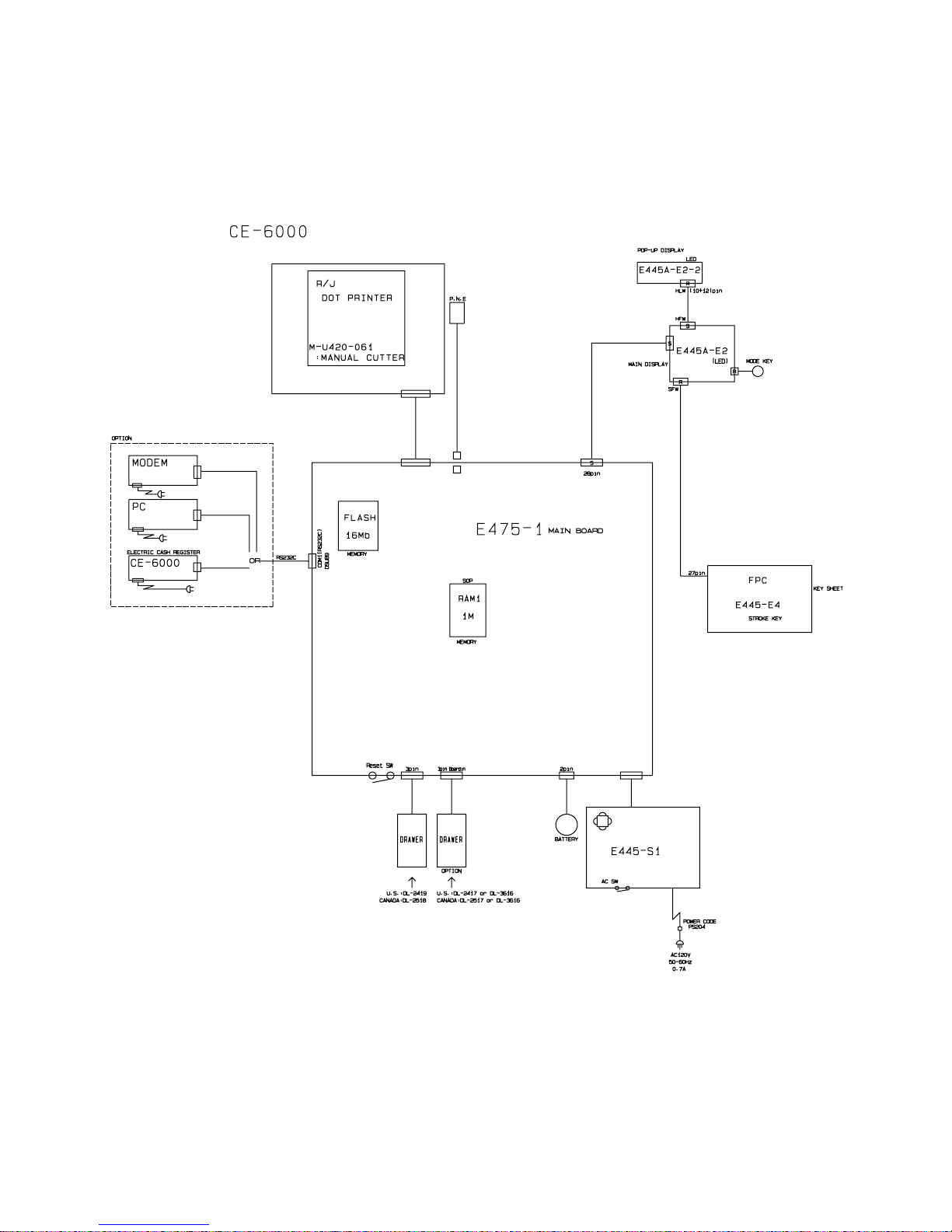
4. BLOCK DIAGRAM
4-1. PCB CONNECTION
— 4 —
Page 7
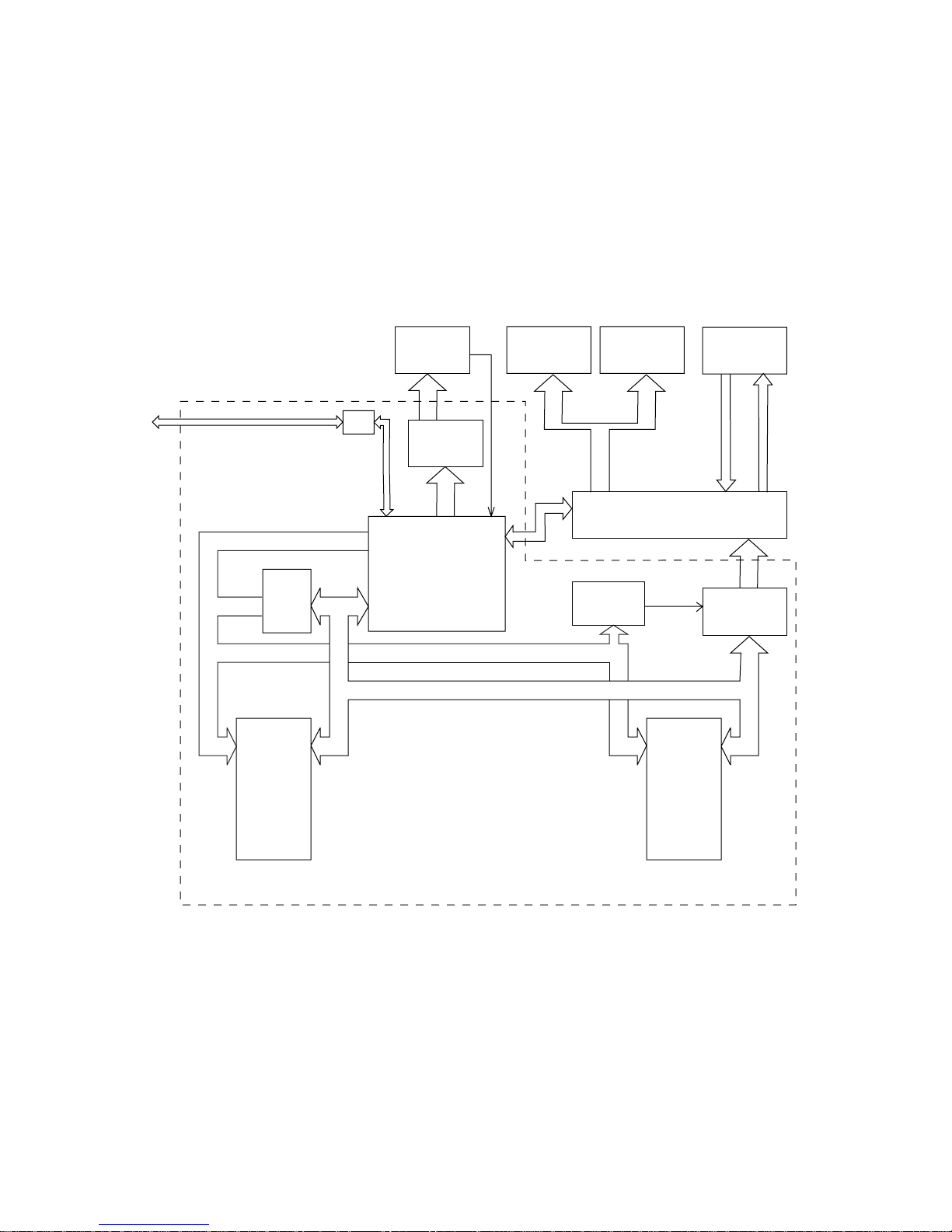
4-2. BLOCK DIAGRAM (CE-6000)
COM1
Address bus A8 - A19
Address
Latch
A0 -A7
RAM1
HY628100A
LLG-70
(128 K bytes)
Printer
M-U420-061
Driver
Data bus D0 -D7
Printer driver
CPU
uPD784215GC-084-8EU
LED display
LED customer
display
LED driver and Key control
I/O selector
Flash ROM 1
LH28F016SCT-L95
(2 M bytes)
Keyboard
Data buffer
MAIN PCB E457-1 C
— 5 —
Page 8
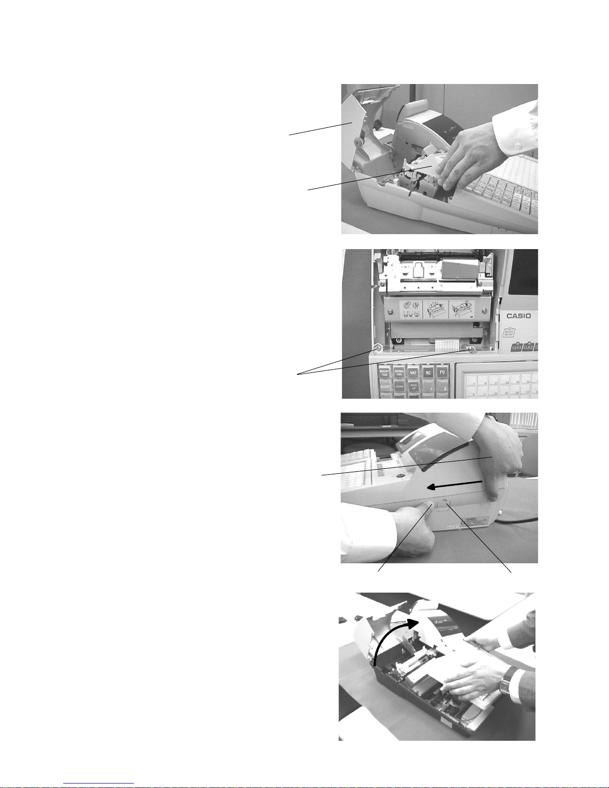
5. TO OPEN THE UPPER CASE
1.Open the printer cover. Then, remove the
ribbon cover from the machine.
2. Remove the 2 screws of the upper case.
Open the printer cover.
Remove the ribbon cover.
Remove the 2 screws.
3. Push the 3 dots marking point at the right
side of lower case. At the same time, slide
the upper case to the front side.
Slide the upper case
to the front side.
4. Open upper cese from the left side.
Press the 3 dots marking point.
Power switch cover
- 6 -
Page 9
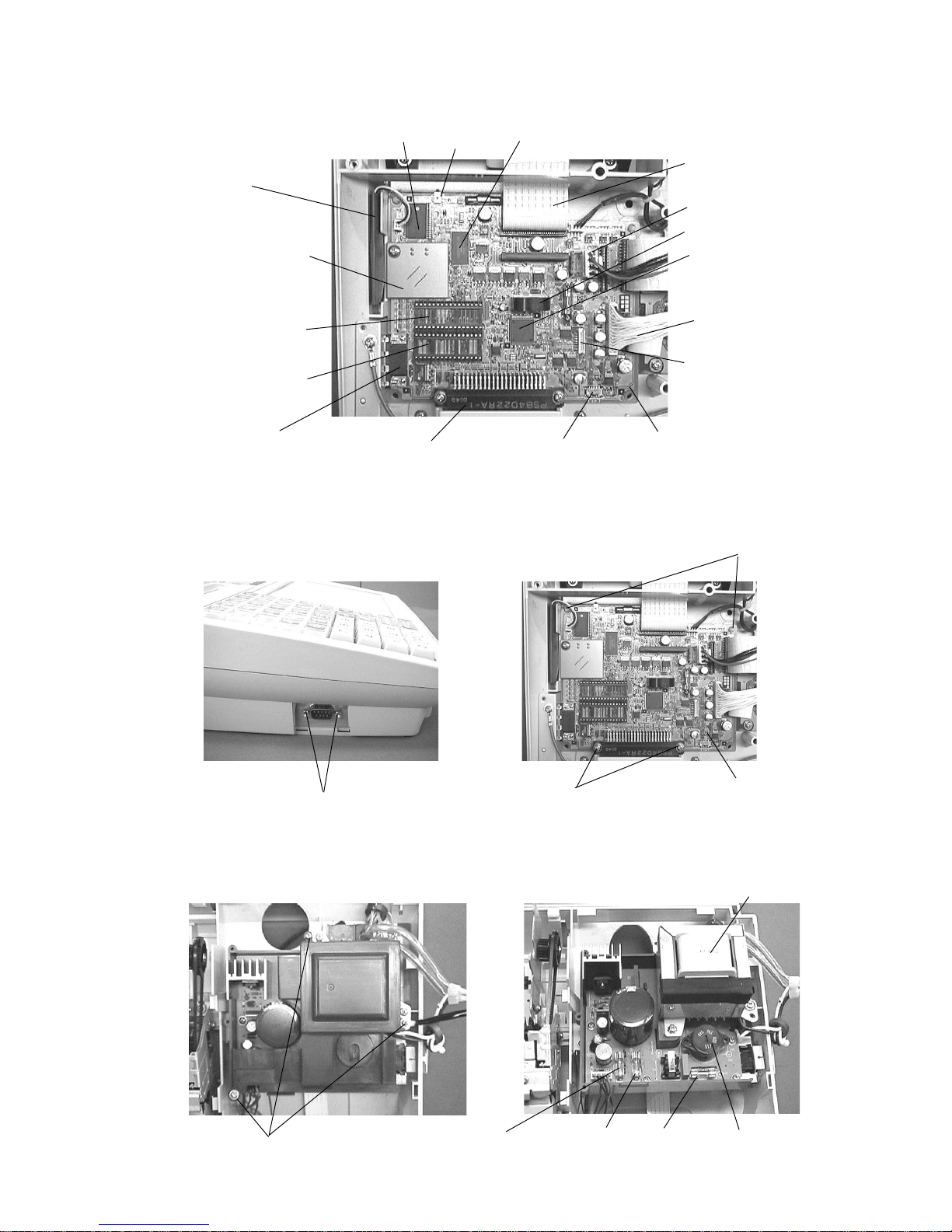
5. The each parts of the Main PCB are located as shown in the picture.
Note: RAM2 is not used for CE-6000.
Flash ROM 1 (2 Mbytes)
Battery
RAM 1 (128 Kbytes)
Reset Switch
Printer cable
Power supply connector
Flash ROM 2
(Not used for CE-6000)
RAM 4
(Not used for CE-6000)
RAM 3
(Not used for CE-6000)
COM 1 port
Flash pack connector
(Not used for CE-6000)
Keyboard select switch
(Not used for CE-6000)
Buzzer
CPU
Display cable
Clerk key connector
(Not used for CE-6000)
Main PCB
6. To remove the Main PCB, release the 2 screws of point A and 2 locking supporters of point B
and the COM1 port outside screws.
Point A
Remove 2 screws.
Remove 2 screws for COM 1 port.
7. Power supply unit cover is removed by 3 screws. And, the 3 Fuses are located as shown in the
picture.
Remove the 3 screws.
Then, remove the power supply cover.
Fuse F3
250V 400mA
(Not used for CE-6000)
- 7 -
Point A
Remove 2 screws.
Fuse F2
250V 2A
Fuse F1
250V 1A
Main PCB
Power transformer
Voltage selector
(Not used for CE-6000)
Page 10
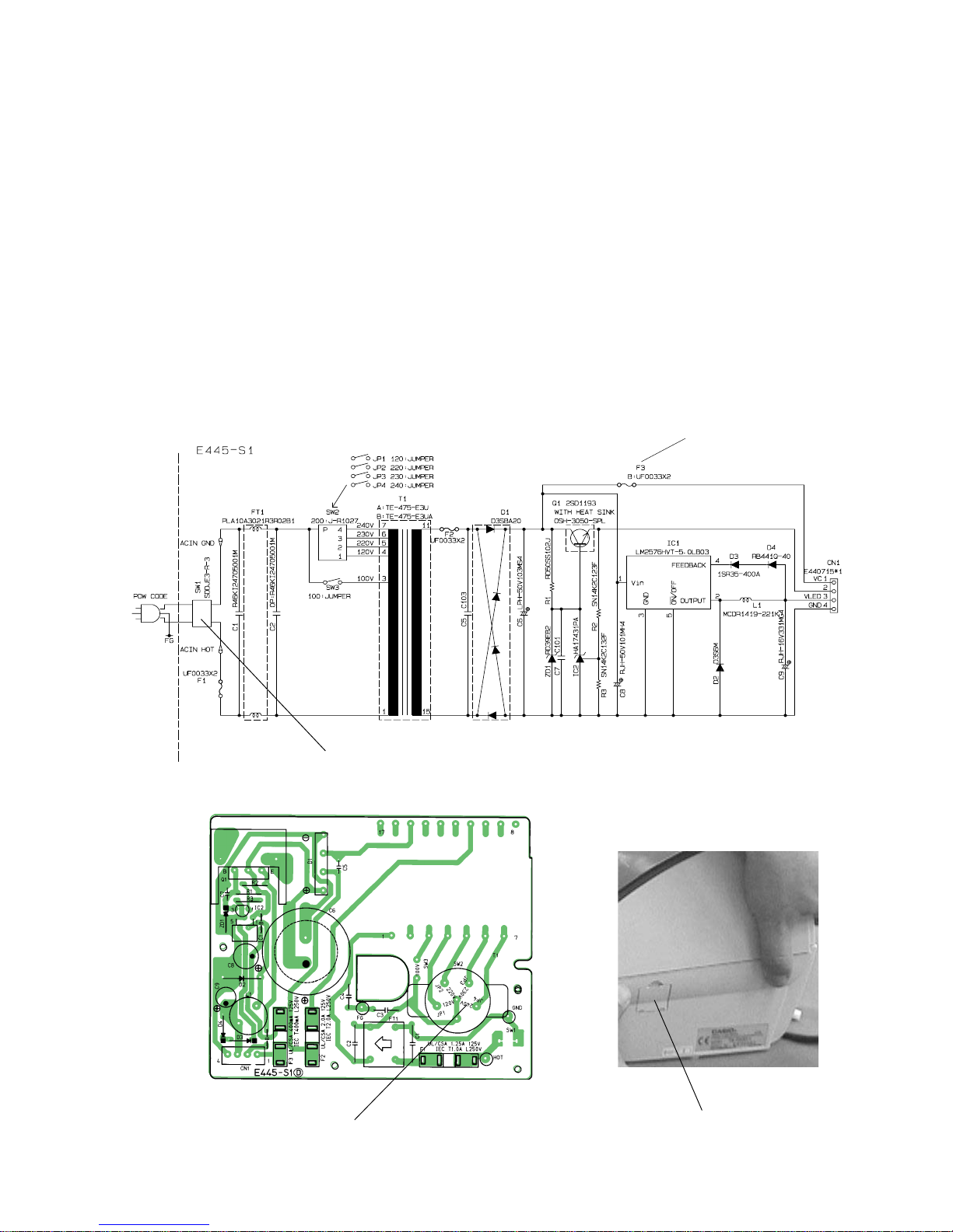
6.CIRCUIT EXPLANATION
6-1. Power supply circuit
The power supply circuit provides the following voltage for the main circuit.
Output Pin No1----- VC1 (DC32.3V): To the VC line for the VFD Display power. (Not used for CE-6000)
Output Pin No.2---- VC2 (DC24V): To the Vp line for the printer power.
Output Pin No.3---- VLED (DC5.85V): To the Vcc,Vcc2 and Vdd for the logic circuit power.
Output Pin No.4---- GND: Signal GND.
The power switch SW1 is located at the right side of the lowercase.
After connected the power plug into AC outlet and turn on the SW1, the transformer T1 will
genarate the about AC33V to secondary side. Then, after rectifier circut, the VC1 (DC32.3V)
is supplied to the VC line for display power (for the drive of display tube. Not for LED model.)
The IC2 is the shunt regulator for the control of Q1 transistor. This circuit is genarate the
VC2 (DC24V) for the printer power. The IC1 is regulator for 5V power supply.
Note: F3 is not used for
CE-6000.
Power switch SW1
Power supply PCB E445-S1
Voltage selector
(Not used for CE-6000)
NOTE: Voltage selector is not used for CE-6000.
Power SW1 cover
- 8 -
Page 11

6-2. Reset and powe down circuit
The rest and power down circuit are as following circuit. The reset switch is provided for the
hard reset to cleare the system error. Use this switch only when the FMAC or MAC are not
possible to perform.
Reset switch
The position of Reset switch
From top of view From rear of view
The mark of reset switch
6-3. CPU pin description(uPD784215GC-084-8EU)
The CPU pin descriptions are as follows:
- 9 -
Printer
Reset switch
Page 12
CPU pin description(uPD784215GC-084-8EU)
Pin No. Signal Name Description In/Out
1 P120 HD1 HEAD PIN DRIVE HD1 Out
2 P121 HD2 HEAD PIN DRIVE HD2 Out
3 P122 HD3 HEAD PIN DRIVE HD3 Out
4 P123 HD4 HEAD PIN DRIVE HD4 Out
5 P124 HD5 HEAD PIN DRIVE HD5 Out
6 P125 HD6 HEAD PIN DRIVE HD6 Out
7 P126 HD7 HEAD PIN DRIVE HD7 Out
8 P127 HDGATE2 HEAD GATE2 Out
9 VD D VDD Power supply VDD +5V
10 X 2 X2 Clock 12.5 MHz In
11 X 1 X1 Clock 12.5 MHz In
12 VS S G ND Power supply GND
13 XT2 XT2 Clock In
14 XT1 XT1 Clock In
15 RESET RESET Reset termial In
16 P00 TP Timing puls from printer TP In
17 P 01 COM2 SEL COM 2 selection Out
18 P02 CUTTER RP Auto-cutter reset pulse CUTTER RP In
19 P 03 PWD Power down signal In
20 P 04 VFD BUSY Display controller busy signal In
21 P05 RP Reset pulse from printer RP In
22 P06 IRQ ARCNET Interrupt rquest form ARCNET controller In
23 A VDD VDD Power supply VDD +5V
24 AVREF0 AVREF0 Connected to VDD +5V
2 5 P10 AVREF Vp voltage check terminal In
26 P11 HDTH Head thermistor input In
27 P12 CROM IN Flash ROM cassette in signal In
28 P 13 DWS Drawer sensor input In
29 P14 DSR1 COM1 DSR signal In
30 P 1 5 CI1 COM1 CI signal In
31 P 16 CD 1 COM1 CD signal In
32 P1 7 P.N.E. Paper near end sensor input In
33 AVSS GND Power supply GND
34 P130 LED SLATCH LED Latch signal Out
35 P131 LED CE LED chip enable signal Out
36 AVREF1 VD D Connected to VDD +5V
37 P 7 0 RX2 COM2 and COM3 receive data In
38 P71 TX2 COM2 and COM3 transmit data Out
39 P 72 RAM ENABLE RAM enable signal Out
40 P 20 RX1 COM1 receive data In
41 P21 TX1 COM1 transmit data Out
42 P 2 2 RTS1 COM1 RTS signal Out
43 P23 MOTOR Motor drive signal Out
44 P 2 4 RTS2 COM2 RTS signal Out
45 P 25 LED SIN LED data in signal In
46 P 26 LED SOUT LED data out signal Out
47 P 27 LED SCK LED SCK signal out Out
48 P 8 0 RB0/CB0 Bank selection RB0/CB0 Out
49 P 8 1 RB1 Bank selection RB1 Out
50 P 8 2 RB2 Bank selection RB2 Out
- 10 -
Page 13
Pin No. Signal Name Description In/Out
51 P 8 3 RB3 Bank selection RB3 Out
52 P 8 4 RB4/CB1 Bank selection RB4/CB1 Out
53 P 85 FB0/CB2 Bank selection FB0/CB2 Out
54 P 8 6 FB1 Bank selection FB1 Out
55 P 87 FB2 Connected to GND
56 P 40 D 0 Data/address bus D0/A0 In/Out
57 P 41 D 1 Data/address bus D1/A1 In/Out
58 P 42 D 2 Data/address bus D2/A2 In/Out
59 P 43 D 3 Data/address bus D3/A3 In/Out
60 P 44 D 4 Data/address bus D4/A4 In/Out
61 P 45 D 5 Data/address bus D5/A5 In/Out
62 P 46 D 6 Data/address bus D6/A6 In/Out
63 P 47 D 7 Data/address bus D7/A7 In/Out
64 P 5 0 A8 Address bus A8 Out
65 P 5 1 A9 Address bus A9 Out
66 P 52 A1 0 Address bus A10 Out
67 P 53 A1 1 Address bus A11 Out
68 P 54 A1 2 Address bus A12 Out
69 P 55 A1 3 Address bus A13 Out
70 P 56 A1 4 Address bus A14 Out
71 P 57 A1 5 Address bus A15 Out
72 VS S GND Power supply GND
73 P 60 A1 6 Address bus A16 Out
74 P 61 A1 7 Address bus A17 Out
75 P 62 A1 8 Address bus A18 Out
76 P 63 A1 9 Address bus A19 Out
77 P 64 RD Read signal Out
78 P 65 WR Write signal Out
7 9 P66 WAIT Wait signal In
80 P67 ASTB Address strobe signal Out
81 V DD VDD Power supply VDD +5V
82 P100 BUZZER Buzzer output signal Out
83 P101 R.FEED Receipt paper feed signal Out
84 P102 J.FEED Journal paper feed signal Out
85 P103 STAMP Stamp signal Out
86 P 30 HDGATE1 Head gate 1 signal Out
87 P 31 FLASH RST Flash reset signal Out
88 P3 2 DTR1 COM1 DTR signal Out
89 P33 CTS1 COM1 CTS signal In
90 P3 4 DTR2 COM2 DTR signal Out
91 P35 HDPLS Head pulse signal In
92 P 36 DW1 Drawer signal 1 Out
93 P 37 DW2 Drawer signal 2 Out
94 TEST GND Connected to GND
95 P 90 MODE SIN Mode switch data in signal In
96 P 91 MODE SCK Mode switch SCK signal Out
97 P 92 MODE SLOAD Mode switch data load signal Out
98 P 93 KI SLOAD Key data load signal Out
99 P94 HD8 HEAD PIN DRIVE HD8 Out
100 P95 HD9 HEAD PIN DRIVE HD9 Out
- 11 -
Page 14
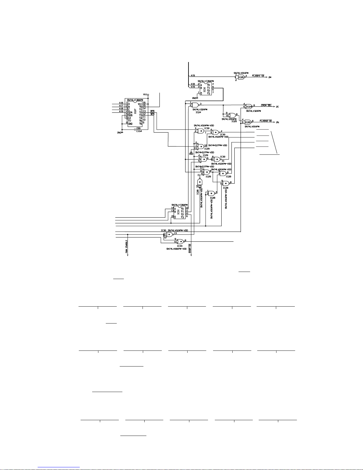
6-4. Memory chip selection circuit
The RAM chip select signals made by the following circuit.
The model CE-6000 uses only RAM1 chip (128 Kbytes). The other RAM chip select signals
are not used.
RAM1 CE
RAM2 CE
RAM3 CE
RAM4 CE
RAM1 CE is for RAM 1 chip
enable signal.
The Model CE-6000 uses only
RAM1.
RB1
RB2
RB3
RB4/CB1
FB1
RAM enable
ARC RESET
RAM1 selection
The RAM1 is selected by the RAM enable signal "H" and the 2CS signal " L" of output pin
No.13 . The 2SC signal becomes "L" when the CPU address is as follows:
A19 A18 A17 A16 A15 A14 A13 A12 A11 A10 A9 A8 A7 A6 A5 A4 A3 A2 A1 A0
L L H L X X X X X X X X X X X X X X X X
2 X X X X
Also, the 3SC signal becomes "L" when the CPU address is as follows:
A19 A18 A17 A16 A15 A14 A13 A12 A11 A10 A9 A8 A7 A6 A5 A4 A3 A2 A1 A0
L L H H X X X X X X X X X X X X X X X X
3 X X X X
Therefore, the RAM1 CE will active when the CPU adress is from 20000H to 3FFFFH with
RAM enable signal "H".
Flash ROM1 selection
The Flash 1 CE will active by the IC25 output pin No.3. This is inverted signal of A19.
A19 A18 A17 A16 A15 A14 A13 A12 A11 A10 A9 A8 A7 A6 A5 A4 A3 A2 A1 A0
H L L L X X X X X X X X X X X X X X X X
8 X X X X
Therefore, the Flash1 CE will active when the CPU adress is from 80000H to FFFFFH.
- 12 -
Page 15
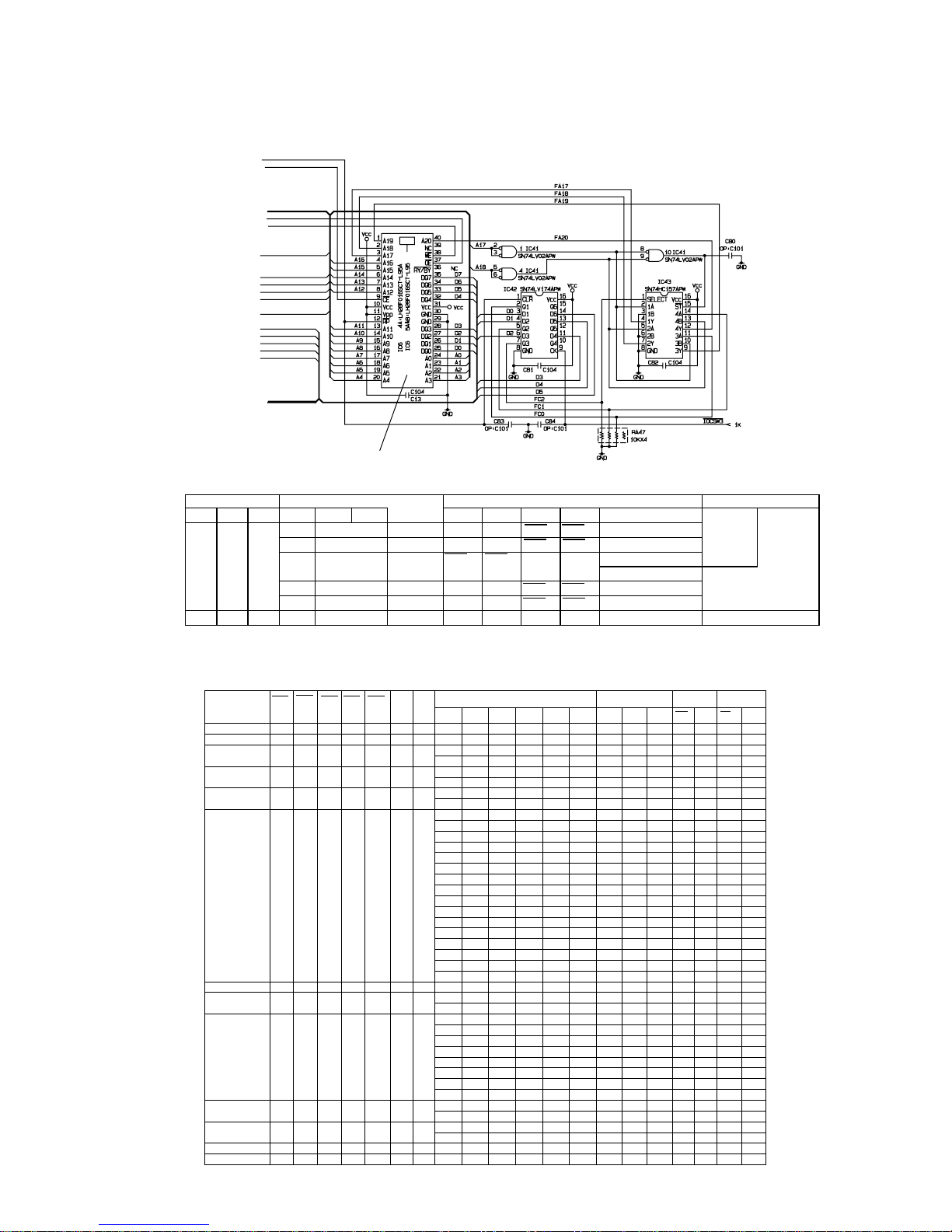
6-5. Flash ROM1 address circuit
The Flash ROM1 address signals FA17 to FA20 are made by the following circuit.
The Flash ROM1 (LH28F016SCT-L95, 16M bits) is used for the application program.
Flash ROM1 (16M bits)
CPU address BANK port Flash memory address NOTE
A19 A18 A17 FC2 FC1 FC0 BANK FA20 FA19 FA18 FA17 Memory block No. 8M bank 16M bank
H L L L L L 0 L L A 1 8 A17 02 to 07
L H L L H 1 L H A18 A17 0A to 0F
H L H X X 2 A18 A17 L L 08,09
L H L 3 H L A18 A17 12 to 17
L H H 4 H H A18 A17 1A to 1F
H H H X X X Common LLLL00,01 Common
10,11,18,19
6-6. Memory map
The memory table is as follows:
RAM enable 2 CS 3C S 4CS 8CS CC S A18 A 19 RAM BANK Flash BANK RAM1 Flash1
H LHHHHLLCOMXXXXXXXXLLHX
H HLHHHLLCOMXXXXXXXXLHHX
H HHLHHHL 0L HL L XXXXHXHX
H HHLHHHL L L HL X XXXHXHX
H HHLHHHL L HHL XXXXHXHX
H HHLHHHL 2LLLHLXXXHXHX
L XXXXXXX XXXXXXXXHXXX
X HHLHHHL HLLLXLHLHXHX
X HHLHHHL LLLLLLLLHXHX
X HHLHHHL XLLLXLXHHXHX
X HHHL HLH XXXXXLXHHXHX
H HHHLHLH XXXXXXXLHXLA18
H HHHHL HH XXXXXXXXHXLA18
No. RB0 RB1 RB2 RB3 RB4 F B0 FB1 FB2 CS A16 CS A18
1HH L L X XXXHXHX
HL HL X XXXHXHX
HHHLXXXXHXHX
3HL L HLXXXHXHX
4L HL HL XXXHXHX
5HH L HL XXXHXHX
6L L HHL XXXHXHX
7HL HHL XXXHXHX
8LHHHLXXXHXHX
9HHHHLXXXHXHX
10L L L H HXXXHXHX
11HLL HHXXXHXHX
12L HL HHXXXHXHX
13HHL HHXXXHXHX
14L L HHHXXXHXHX
15HLHHHXXXHXHX
16LHHHHXXXHXHX
17HHHHHXXXHXHX
HLLLXHHLHXHX
HLLLLLLLHXHX
LLLLHLLLHXHX
HLLLHLLLHXHX
LLLLLHLLHXHX
HLLLLHLLHXHX
LLLLHHLLHXHX
HLLLHHLLHXHX
XLLLXHXHHXHX
XXXXXHXHHXHX
- 13 -
Page 16
Memory map
00000h CPU internal memory
Mask ROM 128K
RAM 5K
0FFD0h External I/O Mapping 16bytes
0FFE0h
20000h
RAM1 128 K bytes
40000h
Not used
80000h
Flash 1 384 K bytes 16 M bit
(for
A0000h Application 8 M bit
program area) 4 M bit
2 M bytes Bank0 Bank1 Bank2 Bank3 Bank4
C0000h
E0000h 04,05 12,13 18,19 24,25 30,31
FFFFFh (00,01)
Bank area
Common area (o3,02) (0B,0A) (09,08) (13,12) (1B,1A)
128 K bytes
Block
06,07
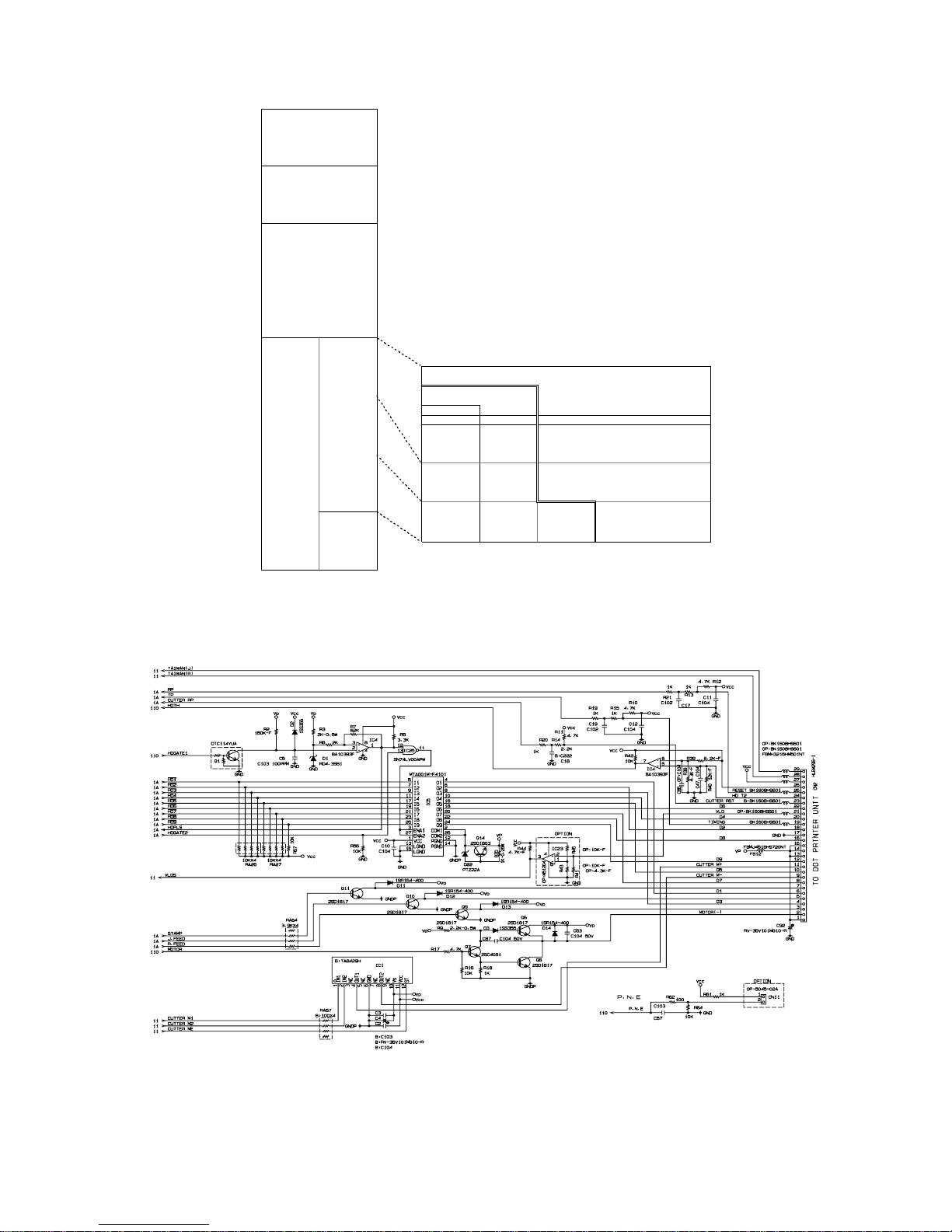
6-7. Printer drive circuit
The printer drive circuit is as follows:
00,01 08,09 14,15 20,21 26,27 Block No.
(07,06) (0F,0E) (19,18) (17,16) (1F,1E) (Memory Block)
02,03 10,11 16,17 22,23 28,29
(05,04) (0D,0C) (11,10) (15,14) (1D,1C)
IC5 (MTA001M-F4101) is the head pin driver. And, the Transistors Q6,Q7 and Q8 are the
motor drive circuit. The IC1 (TA8429H) is the auto paper cut driver circuit. For CE-6000, the
auto paper cut drive circuit is not used.
- 14 -
Page 17
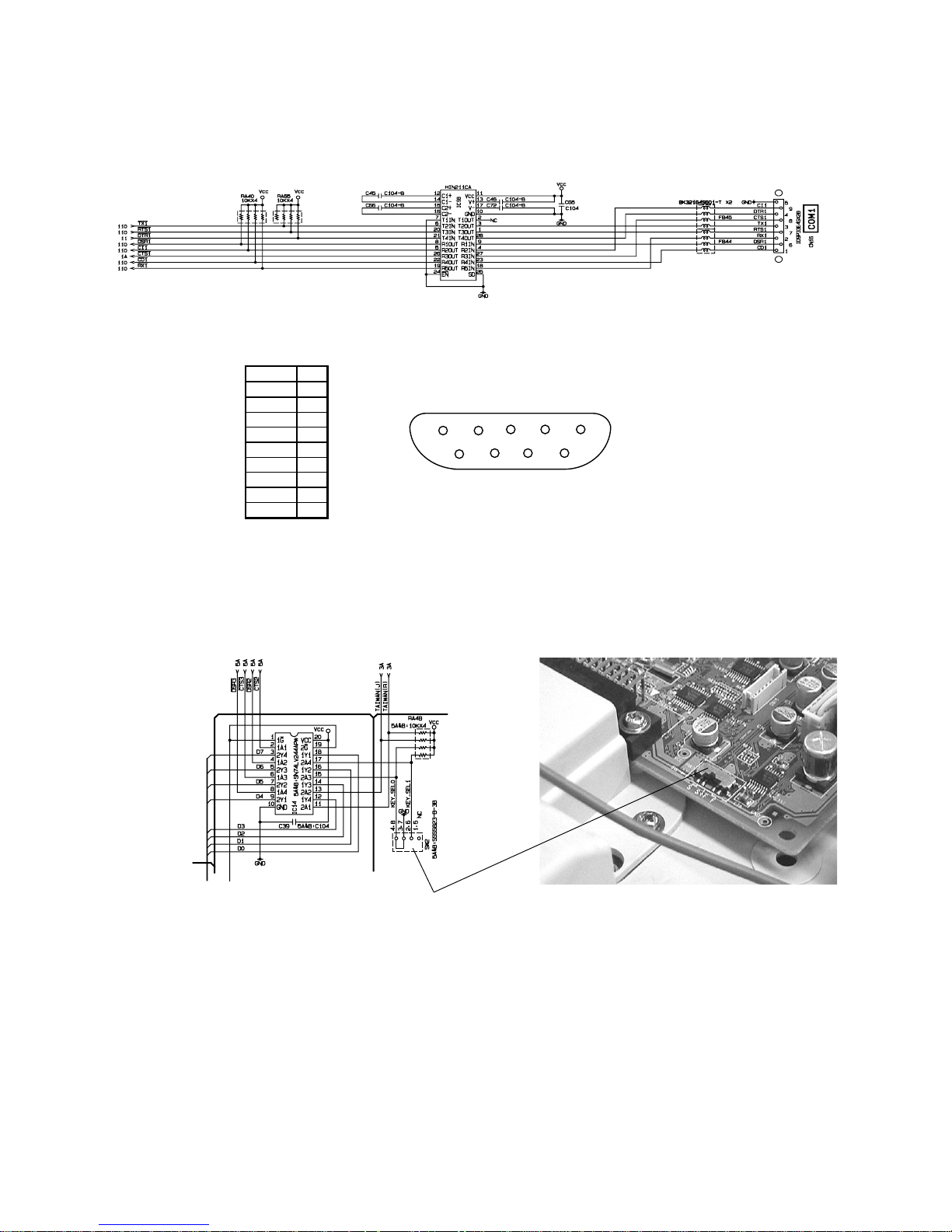
6-8. RS232C port COM1 circuit
The COM1 circuit is as follows:
The COM1 port pin location is as shown below:
Signal Pin
CD 1
RxD 2
TxD 3
DTR 4
GND 5
DSR 6
RTS 7
CTS 8
CI 9
1 2 3 4
6
5
8 9
7
6-9. Keyboard selection switch (Not mounted for CE-6000)
The main PCB has the keyboard selection switch to detect the keyboard type.
For the model CE-6000, the switch is not mounted. It is fixed as a stroke key type.
Keyboard selection switch
(Not mounted for CE-6000)
- 15 -
Page 18
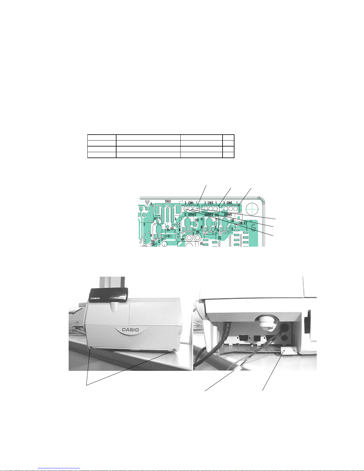
6-10. To mount optional circuit
The following optional circuits are provided for model CE-6000.
1. Multi-drawer circuit
2. Paper near end circuit
1) Multi-drawer kit (Only Drawer 2)
1-1. Prepare the following parts kit for multi-drawer circuit. The parts kits are supplied from sales
division.
MDL-10---------------Multi-drawer kit
1-2. Check whether the parts of clerk kit are as follows:
1-3. Connect the drawer connector cable to the main PCB by solder.
Drawer2
Red
Brown
Black
1-4. Open the back cover of lower cabe to release the 2 screws. Then, connect the necessary
extension cable for drawer. In this case, do no forget to fix the FG wire of the extension
cable to the frame ground plate by the screw.
Release the 2 screws and open the
back cover of lower case.
Connect the extension
drawer cable to the
drawer connector.
Fix the FG wire of the
extension drawer cable by
screw of the parts kit.
1-5. Connect 1 pin FG connector of the drawer extension cable to the drawer 1 pin connector.
Close the back cover of lower case by 2 screws.
Code No. Parts Name Specification Q'ty
10006121 Drawer connector cable E440721A*1 1
62481534 Extension cable for Drawer E440714*1 1
59000209 Screw 3X4ZMC-3. 1
Not used
Not used
— 16 —
Page 19
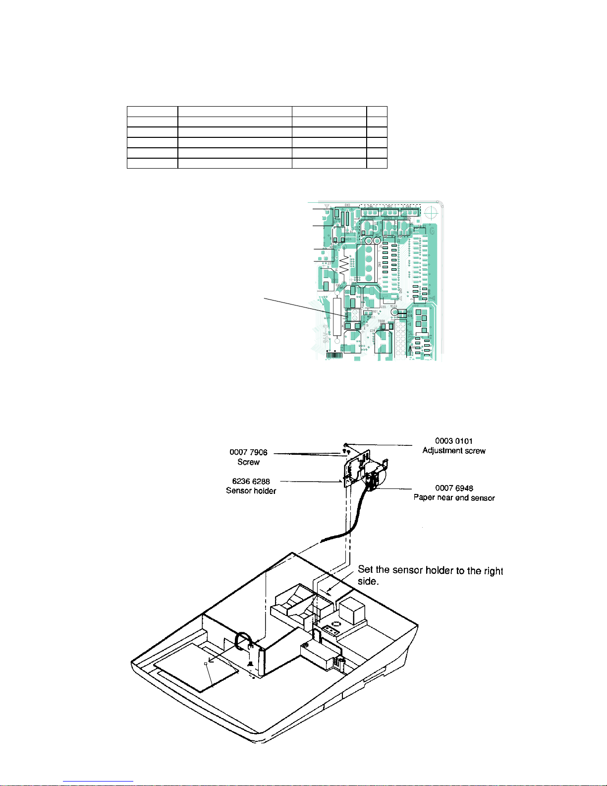
2) Paper near end sensor curcuit
2-1. Prepare the following parts for paper near end sensor circuit. The individual parts are
supplied from Spare parts sales department of CASIO TECNO.
Code No. Parts Name Specification Q'ty
19076948 Paper end sensor C33-651000 1
19030101 Adjustment screw C109302051 1
62366288 Sensor holder E410223B-02 1
19077906 Screw 3 x 8 ZMC-3 2
35401431 Pin assembly 2P 5045-02A 1
2-2. Mount the pin assembly 2P to the main PCB.
Mount 2P Pin
assembly
2-3. Fix the paper near end sensor to the lower case by 2 screws and connect the sensor
connector to the main PCB.
1903 0101
19077906
62366288
Main PCB
2P connector
1907 6948
- 17 -
Page 20
7. DIAGNOSTIC OPERATION
7-1. To start the diagnostic program
1. Plug the power cord into an AC outlet.
2. Set the mode switch to "OFF" position.
3. While pressing the "Jounal feed " button,
turn the mode switch to "PRG" position.
4. Release the "Journal feed" button.
5. Input "99990000" and press "ST" ("#2" key).
6. Diagnostic program is executed.
7-2. Check item
The following test can be checked in the diagnostic test.
1. Key code test
2. Switch status test
3. Individul function test
7-3. Operation of each test
1. Key code test
When pressing a key, the machine displays
DISPLAY
the following key code.
XXX zz
Hard key code
089 090 091 092 093 094
HARD KEY CODE TABLE
095 096 097 098 099 100
RF JF 077 070 068 066 066 060 054 048 042 036 030 024 018
087 082 076 069 067 065 065 059 053 047 041 035 029 023 017
086 081 075 789064 058 052 046 040 034 028 022 015
085 080 074 456063 057 051 045 039 033 027 014 016
Key borad information
11: Stroke Key
10: Stroke + Flat Key
01: Full Flat Key
084 079 073 123062 056 050 044 038 032 026 020 021
083 078 072 0 11 12 061 055 049 043 037 031 025 019 013
Note: "014" button is work for "#2" key. "013" button is work for "#1" key.
- 18 -
Page 21
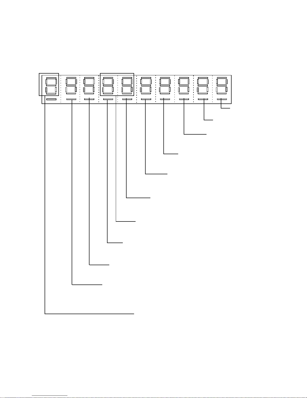
7-4. Switch status test
Press "C" button or changing the switch condition,the switch status is appeared on the
transaction place of the display. The clerk key switch condition is showen at the 6 and 7 digit
number's place of display. For the clerk button model, the pressed LED will light on.
[DISPLAY]
Allways off
Allways off
Allways off
NOTE: Journal TAIWAN sensor
Allways off
NOTE: Receipt TAIWAN sensor
Off: No mark position
On: Mark position
Allways off
NOTE: Validation sensor (Not used)
Off: Normal
On: Validation paper in
Off: No mark position
On: Mark position
ROM cassette condition
Off : Not mounted
On : Mounted
Clerk key condition (Germany)
00 : Not inserted key
01 to 16 : Clerk key number
Paper near end sensor
Off : Normal (Paper end switch OFF)
On : Near end (Paper and switch ON)
Drawer sensor
Off : Drawer close
On : Drawer open
Menu switch conditon (Only for TK6000 and TK7000)
0 : Switchs are both off condition.
1 : Menu 1
2 : Menu 2
Mode switch status
0 : No connetion
1 : PGM
2 : RF
3 : REG1
4 : REG2
5 : X
6 : Z
7 : XZ2
8 : OFF
- 19 -
Page 22
7-5. Individual function test
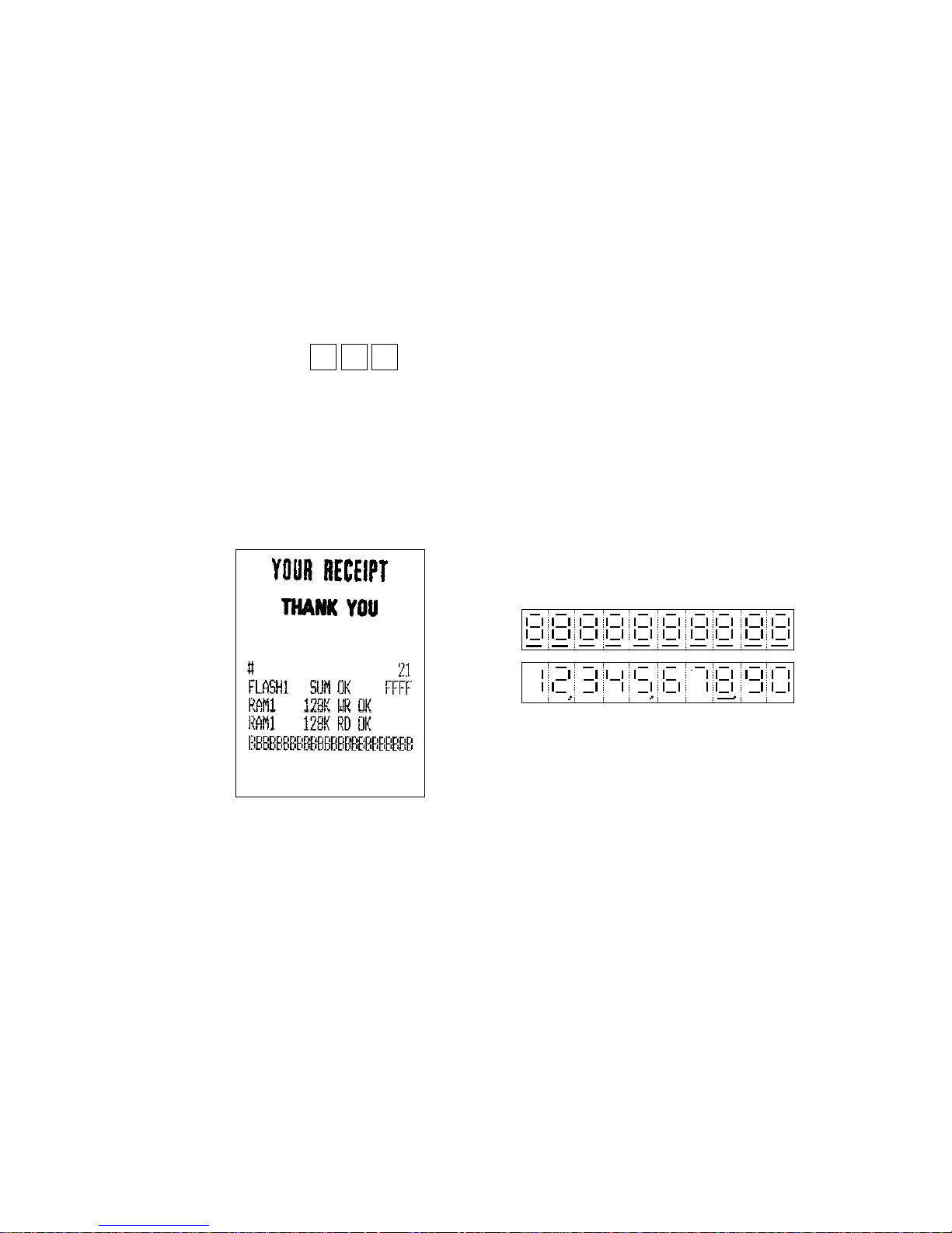
1) Series test
This test will perform the following tests in series.
1. Display test (All dot and segment trun on.)
2. RAM read after write test (one time)
3. Print test (one time)
4. Time display test
5. Drawer open test
6. Receipt issue test
7. Display test (1234567890 display)
Operation : X 1 #2 Key
Function X : 0= Automatic RAM capacity detection
1= RAM1 (128K) test only
NOTE: CE-6000 has the only RAM1 (128 K bytes).
[PRINT] [DISPLAY]
NOTE : In case of error, the following error message will be printed.
RAM1 128K WR ERR!! 00 000000 -----------When the write error is happened.
RAM1 128K RD ERR!! 00 000000 ------------When the verified data error is happened.
FLASH SUM ERR!! 1234 ------------Check sum of Flash1 is not "FFFF".
Error Bank and Address
Caliculated check sum
- 20 -
Page 23

2) Print aging test (R/J printer)
This test will check the R/J printer continuously until pressing some key button or turn off
the mode switch.
Operation : n1 Y X 2 #2 Key
[PRINT] [DISPLAY]
X: 0= Print 45 times test pattern without paper cut in a minute.
1= Print 15 times test pattern with paper cut in a minute.
Y: 0= Normal print
1= Continuously print
n1: 0= Display test pattern
1= All segment will light on.
Segment display (Test pattern)
3) Print test (R/J printer)
This test will check the R/J printer. To stop the continuous printing, press some key
button or turn off the mode switch.
Operation : n1 n 0 X 0 #2 Key
[PRINT] [DISPLAY]
X: 0= One time print
1= Continuously print
n: 0= Display test pattern
1= All segment will light on.
n1: 0= Print test pattern
1= Print all "B"
Segment display (Test pattern)
Print all "B"
Print test pattern
- 21 -
Page 24

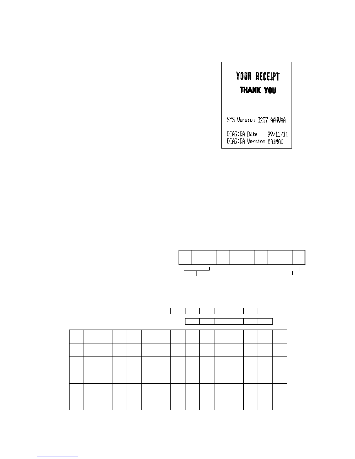
4) Flash1 ROM check
This test will check the Flash 1 ROM. This test will print the version name and check
sum on the receipt as shown in sample print. When using several bank, the each version
name and check sum will be printed after this sample data.
Operation : 9 0 0 #2 Key
[PRINT] [DISPLAY]
5) Drawer open check
This test will check the drawer open function.
Operation : d3 d2 d1 8 n 0 #2 Key
NOTE1: d3,d2,d1 are option drawer test. When input the following number, the option
drawer will be opened.
NOTE2: Command 800 is open drawer1.
n: 0= Open drawer without print.
2= Open drawer with print 10lines "B" printing.
2= drawer2
3= drawer3
4= drawer4
- 22 -
Page 25

6) RAM read only check
This test will check the read only check for RAM.
Perform the RAM check (EX: command "1 and #2 " ), before start of this operation.
Operation : X 5 #2 Key
[PRINT] [DISPLAY]
X: 0= One time check.
1= Continuous check. To stop the test, set the mode switch to OFF.
NOTE: During the RAM test, the Receipt switch LED is blinking.
7) RAM read write check
This test will check the read write check for RAM.
Operation : n 4 X 0 #2 Key
[PRINT] [DISPLAY]
X: 0= Automatic RAM capacity detection
1= RAM1 (128K) test only
n: 1= Continuous check
2= In the continuous check, the print will skip when the test is no error.
4= Read only check. No writing data.
- 23 -
Page 26

8) RS232 port check
This test will check the RS232 port. Connect the loop back connector before operate this
check.
Operation : X 2 m 7 #2 Key
m: 0= One time loop check
1= Loop check continuously
2= One time loop check (Ignore the CD,CI signals. Only COM1 port)
3= Loop check continuously (Ignore the CD,CI signals. Only COM1 port)
X: 0= COM1
Test details
1) Check of the control shignals (CTS,DSR,RTS,DTR,CD,CI) Low/High level.
2) Sending data (0A5h) from Txd line and receiving data from Rxd line.
[PRINT] [DISPLAY]
LOOP BACK CONNECTOR (D-SUB9pin Female)
NOTE: Error code is as follows:
01= Framing error 02= Over run error 04= Parity error
40= Data error (Not 55) 80=Time out error
COM1
TxD
RxD
CTS
RTS
DTR
DSR
CD
CI
3pin
2pin
8pin
7pin
4pin
6pin
1pin
9pin
- 24 -
Page 27

9) Print check
This test will check the print test.
Operation : s 0 0 r 8 #2 Key
NOTE1: To stop this test, press any key or set the mode switch to OFF position.
[PRINT] [DISPLAY]
r: 0= One time check
1= Continuously check (NOTE1)
s: 0= Receipt/Journal print mutually
1= Receipt print only
2= Journal print only
10) All charactor print check
This test will print the all charactors of the controller.
Operation : h h i i 0 s 0 1 r 8 #2 Key
r: 0= Print without code (24 charactors/line)
2= Print with code (16 charactors/line)
4= Print and display without code (24 charactors/line)
6= Print and display with code (16charactors/line)
s: 0= Receipt/Journal print mutually
1= Receipt print only
2= Journal print only
hh: Font selection (High code) ii: Font selection (Low code)
00= USA standard 00= USA
02= Multilingual 01= France
03= Portuguese 02= Germany
04= Canadian-French 03= England
05= Nordic 04= Denmark I
19= Euro+Multilingual 05= Sweden
51= Czecho/Poland 06= Italia
52= Hebrew 07= Spain
53= Greece 09= Norway
54= Russia 10= Denmark II
55= Latvia/Lithuania 51= Czecho/Poland
56= Arabia 52= Hebrew
99= User option 53= Greece
54= Russia
55= Latvia/Lithuania
56= Arabia
99= User option
- 25 -
Page 28

NOTE: When use the command ptrint and display, press #1 key (Cash AMT tender key)
to display and print the next line. To stop this test, press any key or set the mode
switch to OFF position.
[PRINT] [DISPLAY]
11) Time and date display test
The machine will display the time .
By #2 Key, the display will change the date and time.
Opeartion : 9 #2 Key
[PRINT] [DISPLAY]
Press #2 key to change the display.
- 26 -
Page 29

12) Date time set test
The machine will set the time or the date.
Opeartion : n1 n2 n3 n4 n5 n6 X 9 #2 Key
[PRINT] [DISPLAY]
13) COM1 online test
This operation will test the COM1 online function. This test need the reception machine
as shown below;
X: 0= Time set (n1 n2: Time, n3 n4: Minute, n5 n6: Second)
1= Date set (n1 n2: Year, N3 n4: Month, n5 n6: Day)
Send
ECR
Cable length = Max. 15m
COM1 COM1
Receive
ECR
Cross cable
Wiring diagram for the connection cable Loop back connector
Signal Pin Signal Pin
CD 1 CD 1 Txd
RxD 2 RxD 2 Rxd
TxD 3 TxD 3 CTS
DTR 4 DTR 4 RTS
GND 5 GND 5 DTR
DSR 6 DSR 6 DSR
RTS 7 RTS 7 CD
3pin
2pin
8pin
7pin
4pin
6pin
1pin
9pin
CTS 8 CTS 8 CI
CI 9 CI 9
COM1
COM1 COM1
Opeartion : z z b m 7 2 X 7 #2 Key
b: Baud rate selection
0= 19,200 bps 1= 9,600 bps 2= 4,800bps 3= 2,400bps 4= 38,400 bps
m: Test Mode selection
0= Self loop test 1= Reception mode 2= Send mode
ZZ: Time out number (seconds) input between data
(default is 3 seconds. Input ZZ, ZZ seconds will be the time of time out.)
X: 0= Normally select 0.
1= When error is happened, print error receipt before retry operation.
- 27 -
Page 30

Test procedure
1) Operate the send machine first. The send machine will wait the "C" signal (send
request) reception from the reception machine.
The send machine will wait the send request signal about 30 seconds. When it is over
30 seconds, the time out error will be printed on the receipt.
2) Operate the reception machine. Then, the both machines are communicated each
others. This time first block data wait time is 5 seconds. The total resend request time
is 5 time.
3) During communication waiting time, the display will show the "-" brinking on the most
left side digit of segment display. When the data is OK, the reception/transmission
packet number will be displayed on the segment display.
NOTE1: To stop this opeartion, press any or trun off the mode key switch.
NOTE2: The send packet data format is as follows:
( Communication format is 8 bits, even parity, stop bit= 1bit fixed.)
STX
03h
Block counter
2 bytes
Data (55h X 1,020 pcs.)
Total 1,024 bytes
[PRINT] [DISPLAY]
Normal End
Error End (Time out error)
E : Error status
(01 : Framing error)
(02 : Over run error)
(04 : Parity error)
(40: Transmit/ Receive data error/ Data is not 55.)
(80 : Time out error)
LRC
Count data block
7-6. To exit the diagnostic mode
To escape the diagnostic mode, execute INITIALIZE (MAC) operation.
- 28 -
Page 31

8. ERROR CODE
8-1.Operation error code
When an error condition is generated, one of the following error codes (E001 – E153) is
displayed to indicate the cause of the error and the corrective action.
edocrorrEgninaeMnoitcA
100E.noitazilaniferofebdegnahcnoitisophctiwsedoM .noitarepoehtezilanifdnagnitteslanigirostiothctiwsedomehtnruteR
300E
.noitartsigerkcehc
400E.ssergorpninoitareporaelckcoltinuronoitazilaitinI .noitarepoetelpmoC
800E.rebmunkrelcagniretnetuohtiwnoitartsigeR .rebmunkrelcaretnE
900E.drowssapehtgniretnetuohtiwnoitarepO .drowssapretnE
010E
110E.neposirewardhsacehtelihwretsigerottpmettA .rewardhsacehttuhS
610E.edomdnuferehtnidetpmettasnoitcasnartevitucesnocowT
710E.rebmunkcehcagnittupnituohtiwmetinaretsigerotedamtpmettA .rebmunkcehcatupnI
810E.rebmunelbatagnittupnituohtiwmetinaretsigerotedamtpmettA .rebmunelbatatupnI
910E.remotsucforebmunehtgniretnetuohtiwdepmettanoitarepoezilaniF .remotsucforebmunehtretnE
120E.deretsigersiULPdekniltnemtrapedoN .margorpehttcerroC
620E.deretsigersiULPnoitaraperp/tnemidnocoN .ULPnoitaraperp/tnemidnocretsigeR
720E.llufreffublecnacnoitcasnarT .noitcasnartehtezilaniF
920E.rednetlaitrapelihw,detibihorpsinoitartsigermetI .noitcasnartehtezilaniF
030E.xat-etargniretsigertuohtiwnoitcasnartehtezillanifotedamtpmettA<retsigeRXATETAR.>
130E
230E
330E .rednettnuomagniretnetuohtiwdetpmettanoitarepoezilaniF .derednettnuomaehtretnE
530E .timilteserpsdeecxetnuomaegnahC .niagaderednettnuomatupnI
630E .timildemmargorpdeecxerewardehtfostnetnoC .noitarepopukcipmrofreP
730E rorretuokcoltigidwol/tuokcoltnuomahgiH .tnuomatcerrocretnE
830E
040E .tpiecertseugagniussituohtiwnoitcasnartaezilanifotedamtpmettA .tpiecertseugaeussI
140E .demrofreptonsinoitadilaV .noitareponoitadilavmrofreP
640E .llufreffubnoitartsigeR .noitcasnartehtezilaniF
940E .llufyromemxednignikcartkcehC .desuyltnerrucrebmunkcehcehtesolcdnaezilaniF
050E .llufyromemliatedgnikcartkcehC .desuyltnerrucrebmunkcehcehtesolcdnaezilaniF
150E
250E
350E
450E revoegnarrebmunkcehC .rebmuntcerrocretnE
950E .>TUO-EKAT<ro>NI-TAE<gniyficepstuohtiwsmetiretsigeR .>TUO-EKAT<ro>NI-TAE<sserP
570E .oreznahtsselsiecnalabnehwnoitcasnartaezilanifottpmettA .tnuomaevitisoproorezsemocebecnalabehtlitnu)s(metiretsigeR
090E eruliafrevohctiwsoruE .ylreporpnoitareporevohctiwsoruEmrofreP
931E
641E .llufsieliftnemegnarrA .ylreporptnemegnarraehtteS
351E .tessiedocULPmodnaroN .edocULPmodnarteS
.)mralanepo
.latotbus
.latotbuspmatsdoofeht
<esuedamottpmettAKCEHCWENgnisukcehcwenanepoot>
.yromemgnikcart
.desugniebsi
<esuotedamtpmettAKCEHCDLOgnisukcehcwenanepoer>
.yromem
.evitagen
.nottubkrelcrehtonarednudemrofrep
.detavitcasinoitcnufsihtnehwylnosraeppa
gniebnoitartsigerafonoitazilaniferofebdesserpnottubkrelC
gnikcartehtdemrofrepkrelcehtmorfsreffidkrelcnodengisehT
.deneposirewardhsacehtelihwedamsinoitartsigeR
reward(emitmargorpehtnahtregnolnepotfelsirewardehT
ehtgnimrifnoctuohtiwdetpmettanoitcasnartafonoitazilaniF
fognimrifnoctuohtiwdetpmemttanoitcasnartafonoitazilaniF
rorresihT.rewardnihsacgniralcedtuohtiwnoitarepoteser/daeR
kcehcnikcehcgnitsixenarofdesuydaerlasitahtrebmuna
rebmundeificepsehtelihwrebmunkcehcemasehtesuottpmetA
gnikcartkcehcnikcehcgnitsixenarofdesutonsitahtrebmuna
semocebecnalabehtnehw>NPC<ro>–<retsigerottpmettA
.nottubkrelcrehtonagnisserp
.rewardehtesolC
.noitcasnart
.>LATOTBUS<sserP
.>TS/SF<sserP
.noitaralcedyenommrofreP
.rebmunkcehctnereffidaesuroesuottnaw
.rebmunkcehctnereffidaesuroesuottnaw
.kcehcwenanepo
.tnuomanopuoc/sunimreporpretnE
<esuro)yromemgnikcartkcehcnistsixeydaerlaKCEHCWENot>
erofebnoitcasnartehtezilanifdnanottubkrelclanigiroehtsserP
.rebmunkrelcreporpehtngissarorebmunkcehctcerroctupnI
txenehtrofedomFRehtotkcabnehtdnaedomrehtonaothctiwS
uoytahtrebmunehtrednuyltnerrucsitahtkcehcehtesolcdnaezilaniF
uoytahtrebmunehtrednuyltnerrucsitahtkcehcehtesolcdnaezilaniF
tahtkcehcanepoerottnawuoyfi(rebmunkcehctcerrocehtesU
- 29 -
Page 32

9. IC DATA
1. BA10393F-E2 2. BA12003BF-E2
3. HA17431PA
4. HD74LVC374ATELL
- 30 -
Page 33

5. HIN211CA-T
6. HY628100ALLG-70
7. LC7932M-TE-R
- 31 -
Page 34

8. LH28F016SCT-L95A
- 32 -
Page 35

9. LM2576HVT-5.0LB03
10. MTA001M-F4101
- 33 -
Page 36

11. S-80823ANNP-EDL/S-80835ALNP-EAZ
(1) Nch open drain active low output
12. SN74AHC1G00DCKR
(2) CMOS active low output
S-808XX AX XX - XXX - T2
Tape spec. IC direction
Production short No.
Package No.
NP: SC-82AB
MP: SOT-23-5
UP: SOT-89-3
Y: TO-92
Output
N: Nch open drain (Active "L")
L: CMOS (Active "L")
Detection Voltage X 10 times
13. SN74HC157APWR
- 34 -
Page 37

14. SN74HC27PWR
15. SN74LV00APWR
16. SN74LV02APWR
17. SN74LV08APWR
- 35 -
Page 38

18. SN74LV138APWR
19. SN74LV139APWR
- 36 -
Page 39

20. SN74LV165APWR
21. SN74LV165APWR
- 37 -
Page 40

22. SN74LV174APWR
23. SN74LV32APWR
24. SN74LV74APWR
- 38 -
Page 41

10. PCB LAYOUT
MAIN PCB (Front side)
- 39 -
Page 42

MAIN PCB (Back side)
- 40 -
Page 43

11. CIRCUIT DIAGRAM
MODEL : CE-6000 (EX-475A*-M )
CONTENTS
1. LOCATION OF PRINTED CIRCUIT BOARD................................................................... 42
2. MAIN PCB CIRCUIT ........................................................................................................43
2-1. MAIN PCB CIRCUIT (1/6) ........................................................................................ 43
2-2. MAIN PCB CIRCUIT (2/6) ........................................................................................ 44
2-3. MAIN PCB CIRCUIT (3/6) ........................................................................................ 45
2-4. MAIN PCB CIRCUIT (4/6) ........................................................................................ 46
2-5. MAIN PCB CIRCUIT (5/6) ........................................................................................ 47
2-6. MAIN PCB CIRCUIT (6/6) ........................................................................................ 48
3. LED DISPLAY (MAIN DISPLAY)......................................................................................49
3-1. MAIN PCB CIRCUIT (1/3) ........................................................................................ 49
3-2. MAIN PCB CIRCUIT (2/3) ........................................................................................ 50
3-3. MAIN PCB CIRCUIT (3/3) ........................................................................................ 51
4. KEYBOARD......................................................................................................................52
5. POP-UP DISPLAY............................................................................................................53
6. POWER SUPPLY CIRCUIT..............................................................................................54
7. MODE SWITCH................................................................................................................55
- 41 -
Page 44

- 42 -
Page 45

- 43 -
Page 46

- 44 -
For CE6000, the RAM2,RAM3, and RAM4 are not used.
For CE6000, the Flash ROM2 is not used.
Page 47

- 45 -
Page 48

- 46 -
Page 49

- 47 -
T
For CE6000, COM2 and COM3 are
not used.
Page 50

- 48 -
Page 51

- 49 -
Page 52

- 50 -
Page 53

- 51 -
Page 54

- 52 -
Page 55

- 53 -
Page 56

- 54 -
Voltage selector is not used for CE-6000.
Page 57

- 55 -
Page 58

12. PARTS LIST
CONTENTS
Explode view ................................................................................................................... 57
1. MAIN PCB BLOCK ....................................................................................................... 59
2. MAIN DISPLAY BLOCK ............................................................................................... 60
3. CUSTOMER DISPLAY BLOCK.................................................................................... 60
4. BUTTON BLOCK ......................................................................................................... 61
5. POWER SUPPLY BLOCK............................................................................................ 62
6. UPPER CASE BLOCK.................................................................................................. 63
7. LOWER CASE BLOCK................................................................................................. 63
P AR TS LIST
MODEL : CE-6000 (EX-475A*-M)
8. PRINTER BLOCK......................................................................................................... 64
9. OTHERS ......................................................................................................................64
10. PRINTER (M-U420-061)............................................................................................. 64
11. DRAWER ................................................................................................................... 64
DL-2419 USA.............................................................................................................. 67
DL-2518 CANADA...................................................................................................... 69
NOTES :
1. Price and specifications are subject to change withput prior notice.
2. As for spare parts order and supply, refer to the “GUIDEBOOK for Spare Parts Supply”,
published separately.
3. The numbers in item column corespond to the same numbers in drawing.
4. CASIO does not supply the spare parts without parts code.
5. Remarks
Q'ty : Quantity used per unit
RANK: A = Essential
B = Stock recommended
C = Less recommended
X = No stock recommended
- 56 -
Page 59

11
6
7
LED -
5
Numeric LED
4
PCB Blank
3
79
54
CASIO CE-6000
37
55
48
55
10
8
9
50
83
82
47
2
51
49
39
35
30
34
14
12
33
22
20
32
9
8
6
7
5
3
4
2
.
1
00
0
31
28
27
13
23
29
26
25
24
36
17
18
15
16
38
21
19
- 57 -
Page 60

69A
52
53
66
42
69A
40
46
74
43
76
77
78
41
70
73
82
69A
75
72
71
69
63
60
61
62
82
81
1
65
67
59
58
Battery only
57
64
69B
65
65
67
80
68
69B
84
For Drawer fix
- 58 -
Page 61

- 59 -
Page 62

- 60 -
Page 63

- 61 -
Page 64

- 62 -
Page 65

- 63 -
Page 66

131
907
504
505
506
502
501
503
507
509
508
114
RIBBON CASSET
140
148
145
139
141
516
112
519
105
109
901
110
902
905
119
125
115
130
124
108
135
129
128
539
544
542
545
130
136
102
113
510
511
513
514
138
133
147
132
527
522
103
525
536
523
521
536
525
525
520
524
540
535
541
537
528
526
543
532
531
529
539
534
538
532
533
531
530
903
904
906
118
116
117
122
121
123
120
126
906
127
510
102
146
101
137
142
134
104
517
518
107
106
111
515
512
"The exploded diagram is made based on the standard specification of our company.
When the part or unit indifferent form your specification is shown in the diagram,please
disregard it."
EXPLODED DIAGRAM FOR M-U420-061 REV. 2
10. PRINTER (M-U420-061)
- 64 -
Page 67

PARTS PRICE LIST
M-U420(061)
N Item Code No. Parts Name Specification Q Price Code R
1. DRIVING MECHANISM COMPONENTS
101 19092776 LEVER/FIXING J 1004032 1 AE C
102 19092777 SPRING/FIXING LEVER 1004033 2 AC C
103 19092775 LEVER/FIXING R 1004031 1 AE C
N 104 94870506 MAIN MOTOR ASSY 1049277 1 BV A
N 105 94870505 GEAR/MAIN MOTOR 1049273 1 AB B
106 19060719 WIRE/LEAD A 2021071 1 AA X
107 19060720 WIRE/LEAD B 2021072 1 AA X
108 19060721 SCREW M2.6X4 F/NI 1006328 2 AA X
109 19060722 DETECTOR ASSY/TIMING 1028549 1 BI B
110 19087657 SCREW M3X5 B300204111 1 AA X
111 19060723 SHAFT/RIBBON DRIVE ASSY 1028550 1 AZ X
112 19060724 FRAME/BACK 1027999 1 AO X
113 19085554 SCREW M3X5 B300304111 1 AA X
114 19060725 CLAMP/MINI(UAMS-05-0) 1029197 1 AA X
115 19060726 FRAME SUB ASSY/GEAR TRAIN 1028553 1 AA B
116 19060727 GEAR/TRANSMISSION PAPER TAKE-UP 1028012 1 AD B
117 19060728 FLANGE/TAKE-UP TRANSMISSION 1028015 1 AB B
118 19060729 GEAR/PAPER FEED TRANSMISSION 1028016 1 AE B
119 19030118 BELT/PAPER TAKE-UP F701009020 1 AS B
120 19060730 GEAR/DECELERATION CARRIAGE 1028031 1 AH B
121 19060731 GEAR/TRANSMISSION 1028009 1 AB B
122 19060802 GEAR/DECELERATION 1028011 1 AC B
123 19060732 GEAR/TRANSMISSION CARRIAGE 1028010 1 AD B
124 19060733 GEAR/RIBBON DECELERATION 1028056 1 AG B
125 19085554 SCREW M3X5 B300304111 2 AA X
N 126 94870504 GEAR/TIMING DETECTION 1049274 1 AB B
127 19092805 RING/RETAINING TYPE-E(2.5) 1004399 1 AA C
128 19060803 FRAME/GUIDE 1028001 1 AI X
129 19060735 PLATE/RESET SIGNAL ADJUSTMENT 1028032 1 AB X
130 19085554 SCREW M3X5 B300304111 2 AA X
131 94870281 MAIN BOARD ASSY 1043913 1 BP C
132 19060737 PRINT HEAD ASSY/FPC 1028557 1 BT A
133 19085554 SCREW M3X5 B300304111 1 AA X
134 19060738 CARRIAGE ASSY 1028558 1 BJ C
135 19060739 SHAFT/CARRIAGE GUIDE 1028022 1 AT X
136 19092805 RING/RETAINING TYPE-E(2.5) 1004399 1 AA C
137 19060740 SCREW 1012350 1 AA X
138 19060740 SCREW 1012350 1 AA X
139 19060741 HEAD COVER ASSY 1031212 1 BD X
140 19085554 SCREW M3X5 B300304111 2 AA X
N 141 94870512 COVER SUB ASSY/PAPER FEED 1059878 1 AQ C
142 19060742 PRINT HEAD UNIT AB 1028577 1 DA A
145 19060770 SCREW 1024130 2 AA X
146 19071217 SPRING/PAPER FEEDING TRIGGER F701251080 1 AB B
147 94870283 CAPACITOR/CHIP 2021922 1 AA X
148 19092847 SEAL/CAUTION 1007667 1 AJ X
N 149 94870507 GEAR/MOTOR ASSY 1052543 1 AB B
N 150 94870508 MAIN MOTOR ASSY 1052544 1 BV A
2. PAPER FEEDING MACHANISM COMPONENTS
501 19060744 PAPER GUIDE/LOWER ASSY 1028537 1 AY X
502 19060745 LEVER/STAMP 1028064 1 AF C
503 19060746 LEVER/STAMP TRANSMISSION 1028059 1 AB C
504 19060747 SPRING/STAMP FORCE ADJUSTMENT 1028063 1 AB C
505 19060748 LEVER/STAMP DRIVE 1028060 1 AD C
506 19060749 SPRING/STAMP RETURN 1028062 1 AA C
507 19060750 PLATE/VALIDATION STOPPER 1028036 1 AC X
508 19060751 GUIDE/VALIDATION 1028044 1 AM C
509 19060740 SCREW 1012350 2 AA X
510 19060740 SCREW 1012350 2 AA X
511 19060752 PLATE SUB ASSY/DRIVEN 1028539 1 AK C
512 19060753 PULLEY/CARRIAGE DRIVEN 1028025 1 AC B
- 65 -
Page 68

PARTS PRICE LIST
M-U420(061)
N Item Code No. Parts Name Specification Q Price Code R
513 19060754 FLANGE/PULLEY 1028027 1 AB B
514 19092805 RING/RETAINING TYPE-E(2.5) 1004399 1 AA C
515 19064056 SCREW M3X3 B040350511 1 AA X
516 19060755 BELT ASSY/TIMING CARRIAGE DRIVE 1028540 1 BE B
517 19060756 PULLEY/CARRIAGE DRIVEN 1028030 1 AD B
518 19060754 FLANGE/PULLEY 1028027 1 AB B
519 19092805 RING/RETAINING TYPE-E(2.5) 1004399 1 AA C
N 520 94870284 YOKE/PAPER FEED TRIGGER 1045794 1 AL C
521 19060758 COIL/PAPER FEED TRIGGER PRT 2021086 1 AS C
522 19060759 COIL/PAPER FEED TRIGGER JNL 2021087 1 AS C
523 19060760 COIL/STAMP DRIVE 2021088 1 AS C
524 19060761 PLATE/PAPER FEED TRIGGER 1028043 3 AE X
525 19071217 SPRING/PAPER FEED TRIGGER F701251080 3 AB C
526 19060762 PLATEN ASSY 1028543 1 AS C
527 19060763 SHAFT/PAPER FEED ASSY 1028544 1 CH A
N 528 94870513 SHAFT/PAPER EXTENSION ASSY 1059877 1 BF C
529 19060804 SHAFT/PAPER FEED PRESSURE 1028046 1 AL X
530 19060765 PLATE/PAPER GUIDE 1028048 2 AM C
N 531 94870510 ROLLER/PAPER HOLD 1052541 2 AE B
532 19092805 RING/RETAINING TYPE-E(2.5) 1004399 4 AA C
533 19060767 SPRING/PAPER GUIDE PLATE 1028049 1 AE C
N 534 94870514 PAPER GUIDE/UPPER SET 1061952 1 AW C
535 19060769 PLATE/PAPER FEED GROUND 1028053 1 AF C
536 19060770 SCREW 1024130 3 AA X
537 19062203 SCREW M3X8 B312104311 2 AA X
N 538 94870548 EXIT ASSY/PAPER GUIDE 1063432 1 AM C
539 19060772 SPRING/PAPER FEED PRESSURE 1028047 2 AB C
540 19060773 LEVER/RELEASE PRT 1028050 1 AD C
541 19030715 RING/RETAINING B150300711 1 AA C
542 19060774 LEVER/RELEASE JNL 1028051 1 AD C
543 19092805 RING/RETAINING TYPE-E(2.5) 1004399 1 AA C
544 19060775 GEAR/PAPER FEED 1028038 1 AC B
545 19060776 GEAR/PAPER EXTENSION SHAFT 1028054 1 AB B
546 19060777 ROLLER/PAPER HOLD 1037340 1 AL B
547 19060778 SPACER/PAPER HOLD ROLLER 1037341 1 AQ C
3. PAPER TAKE UP MECHANISM COMPONENTS
901 19060799 FRAME SUB ASSY/TAKE-UP 1028548 1 AS X
902 19060800 PULLEY/TAKE-UP DRIVE 1028102 1 AD B
N 903 94870285 SPRING/TAKE UP TORQUE 1042651 1 AK B
904 19091688 GEAR/PAPER TAKE-UP DRIVE F750302030 1 AD B
905 19030787 RING/RETAINING TYPE-E(3) B150300611 1 AA C
906 19085554 SCREW M3X5 B300304111 2 AA X
907 19060801 SHAFT/PAPER ROLLING 1012719 1 BD X
- 66 -
Page 69

11. DRAWER
DL-2419 (U.S.A.)
- 67 -
Page 70

DL-2419 (U.S.A.)
N Item Code No. Parts name Specification Q'ty Price Code RANK
2 19061309 CHASSIS/BOTTOM 264D-1101 1 CW X
3 55000619 ROLLER/DERLIN DR-19-B1 1 AG B
4 55000878 ROLLER/DERLIN DR-19-B2 3 AP B
N 5 19079682 WASHER SW-M6 2 AA X
6 19077150 NUT HN-M6 2 AA X
7 19081339 BRACKET/LOCK 37A-B150 1 BL X
N 8 94870387 SOLENOID 262A-S154C 1 CD B
N 9 94870400 TIE/INSULOCK P12-1555 1 AA X
N 10 94870395 BRACKET/SHAFT GUIDE 808R-1910 1 BH X
N 11 94870397 SCREW CP-M2.3X10 2 AA X
N 12 94870413 SPRING/MICRO SWITCH S808-1557 1 AC C
N 13 94870398 SCREW CPS-M3X5 2 AA X
N 14 19064013 SCREW CPST-M2.6X6 2 AA X
15 19083432 SPRING/LOCK S37-1551 1 AV C
N 16 19064014 SPRING/DRAWER S40-1351 1 AW C
N 17 19081343 HOLDER/SPRING 44A-1302 1 AW B
N 18 94870405 RUBBER/STOPPER R37-1561 1 AD X
N 19 19077157 WASHER PW-M4 1 AA X
N 20 19027095 SCREW M4X12 1 AA X
N 21 94870399 SCREW CPS-M4X6 3 AA X
N 22 19064017 RUBBER/STOPPER 262A-1651 2 AN X
N 23 19059570 FOOT/RUBBER NR33-1461 4 AD X
N 24 94870396 SCREW CCST-M4X12 4 AA X
N 25 19064018 EARTH/LEAF SPRING 33V-1103 1 AN X
N 26 19064008 SCREW CCST-M3X6 1 AA X
N 27 19081358 SCREW CPST-M3X6 5 AA X
N 28 94870389 DRAWER 262D-2100 1 CM X
29 19077153 SHAFT/HOLDER 12H-5339 1 AD X
N 30 19074264 RING/M4E M4 1 AA X
N 31 94870412 SPONGE R16-2650 1 AD X
N 32 94870390 PANEL/FRONT 262D-2401 1 BH X
33 19077147 LOCK/CYLINDER HL-C168L 1 AV C
34 19077146 KEY/CYLINDER LOCK HL-C168K 2 AU C
35 19077145 CLIP 168-2552 1 AJ X
N 36 19079657 WASHER/LOCK KEY PW-2506 1 AF X
N 37 94870401 CASE/MONEY P16-4160 1 BK C
N 38 94870402
PLATE/MONEY CASE PART
P16-4162 4 AD C
N 39 94870403 CASE/COIN P16-4163 1 AX C
N 40 94870404
PLATE/COIN CASE PARTIT
P16-4164 4 AF C
N 41 19081308 BRACKET/BILL HOLDER 16C-4201 1 AS X
42 19074278 STOPPER/BILL HOLDER 13C-4202 5 AH X
43 19074279 HOLDER/BILL 16B-4203 5 AG B
44 19074280 SPRING/BILL HOLDER S16-4254 5 AA B
N 45 19074281 SCREW CPTS-M3X5L 5 AA X
N 46 19074282 SCREW CPTS-M3X6 3 AA X
N 47 94870407 LABEL/DRAWER PO-2419 1 AC X
- 68 -
Page 71

DL-2518 (CANADA)
- 69 -
Page 72

DL-2518 (CANADA)
N Item Code No. Parts name Specification Q'ty Price Code RANK
2 19061309 CHASSIS/BOTTOM 264D-1101 1 CW X
3 55000619 ROLLER/DERLIN DR-19-B1 1 AG B
4 55000878 ROLLER/DERLIN DR-19-B2 3 AP B
N 5 19079682 WASHER SW-M6 2 AA X
6 19077150 NUT HN-M6 2 AA X
7 19081339 BRACKET/LOCK 37A-B150 1 BL X
N 8 94870387 SOLENOID 262A-S154C 1 CD B
N 9 94870400 TIE/INSULOCK P12-1555 1 AA X
N 10 94870395 BRACKET/SHAFT GUIDE 808R-1910 1 BH X
N 11 94870397 SCREW CP-M2.3X10 2 AA X
N 12 94870413 SPRING/MICRO SWITCH S808-1557 1 AC C
N 13 94870398 SCREW CPS-M3X5 2 AA X
N 14 19064013 SCREW CPST-M2.6X6 2 AA X
15 19083432 SPRING/LOCK S37-1551 1 AV C
N 16 19064014 SPRING/DRAWER S40-1351 1 AW C
N 17 19081343 HOLDER/SPRING 44A-1302 1 AW B
N 18 94870405 RUBBER/STOPPER R37-1561 1 AD X
N 19 19077157 WASHER PW-M4 1 AA X
N 20 19027095 SCREW M4X12 1 AA X
N 21 94870399 SCREW CPS-M4X6 3 AA X
N 22 19064017 RUBBER/STOPPER 262A-1651 2 AN X
N 23 19059570 FOOT/RUBBER NR33-1461 4 AD X
N 24 94870396 SCREW CCST-M4X12 4 AA X
N 25 19064018 EARTH/LEAF SPRING 33V-1103 1 AN X
N 26 19064008 SCREW CCST-M3X6 1 AA X
N 27 19081358 SCREW CPST-M3X6 5 AA X
N 28 94870391 DRAWER 264C-2100 1 CM X
29 19077153 SHAFT/HOLDER 12H-5339 1 AD X
N 30 19074264 RING/M4E M4 1 AA X
N 31 94870393 CUSHION/TRAY 264D-2651 2 AE X
N 32 94870388 PANEL/FRONT 262B-2401CY 1 BH X
33 19077147 LOCK/CYLINDER HL-C168L 1 AV C
34 19077146 KEY/CYLINDER LOCK HL-C168K 2 AU C
35 19077145 CLIP 168-2552 1 AJ X
N 36 19079657 WASHER/LOCK KEY PW-2506 1 AF X
N 37 94870386 CASE/MONEY 262A-4181 1 BL C
38 19079659
PLATE/MONEY CASE PART
70-9602 3 AE C
39 19079660 CASE/COIN P16-4183 1 AR C
40 19064021
PLATE/COIN CASE PARTIT
P16-4184 4 BJ C
N 41 19081308 BRACKET/BILL HOLDER 16C-4201 1 AS X
42 19074278 STOPPER/BILL HOLDER 13C-4202 4 AH X
43 19074279 HOLDER/BILL 16B-4203 4 AG B
44 19074280 SPRING/BILL HOLDER S16-4254 4 AA B
N 45 19074281 SCREW CPTS-M3X5L 4 AA X
N 46 19074282 SCREW CPTS-M3X6 3 AA X
N 47 94870409 LABEL/DRAWER PO-2518 1 AC X
- 70 -
Page 73

CASIO TECHNO CO.,LTD.
Overseas Service Division
Nishi-Shinjuku Kimuraya Bldg. 1F
5-25, Nishi-Shinjuku 7-Chome
Shinjuku-ku, Tokyo 160-0023, Japan
 Loading...