

Page 1
SERVICE MANUAL
INDEX
(without price)
ELECTRONIC CASH REGISTER
PCR-260B (EX-268EC)
MAR. 2003
Printer Model : M-42V
Page 2

CONTENTS
PCR260B Page
1. SPECIFICATIONS........................................................................................ 1
2. INITIALIZE (MAC) OPERATION.................................................................. 2
3. BLOCK DIAGRAM....................................................................................... 3
3-1. PCB CONNECTION..................................................................................................... 3
3-2. BLOCK DIAGRAM....................................................................................................... 4
4. DISASSEMBLY............................................................................................ 5
5. CIRCUIT EXPLANATION ............................................................................ 8
5-1. Power supply circuit .................................................................................................. 8
5-2. Reset circuit ................................................................................................................ 9
5-4. Printer drive circuit................................................................................................... 10
5-5. Pin description (CPU uPD78044FGF) ..................................................................... 10
6. DIAGNOSTIC OPERATIONS .................................................................... 12
6-1. To start the diagnostic operation............................................................................ 12
6-2. Check items .............................................................................................................. 12
6-3. Operations................................................................................................................. 13
7. ERROR CODE LIST................................................................................... 16
7-1. Operation error code................................................................................................ 16
8. IC DATA ..................................................................................................... 17
9. PCB LAYOUT ............................................................................................ 18
10. CIRCUIT DIAGRAM ................................................................................... 19
11. PARTS LIST............................................................................................... 25
Page 3

1. SPECIFICATIONS
1-1. Electrical specifications
• Power consumption In operation Max. 0.11 A
Power OFF 0.06 A
• Memory protection Back-up battery Mangan Battery (UM-3 × 3 pcs)
Back-up period 1 year (25 °C)
Battery life Replace the battery every 1 years.
• Clock & Calendar Accuracy Within ± 30 sec. per month
Auto calendar Effective until 2099 A.D.
1-2. Environmental specifications
• Operating temperature 0 °C ~ 40 °C
• Operating humidity 10 % ~ 90 %
120V
Min. 0.09 A
• Storage temperature -25 °C ~ 65 °C
• Storage humidity 10 % ~ 95 %
• Vibration strength 1.5 G (The machine must be in the carton box)
1-3. Main components
• CPU Name µPD78044FGF177-3B9
Number of control bit 8bit
RAM (Built-in) 624 Kbits
• Printer Name M-42V-001-060MA
Print method Print wheel selecting type serial printer
MCBF 700,000 lines
Life
• Roll paper Type Fine-quality paper
Size Width 57.5 ± 0.5 mm
Roll diameter 80 mm or less
— 1 —
Page 4
1-4. Drawer List
DRAWER NAME Specification NOTE
• DL-1325 (S type) D-14C2M-D54RP-9* USA
1-5. Option List
DEVICE NAME MODEL NOTE
• Wet cover WT-80
• INK ROLL IR-40
CAUTION
Danger of explosion if battery is incorrectly replaced.
Replace only with the same or equivalent type
recommended by the manufacturer.
Dispose of used batteries according
to the manufacture’s instructions.
VORSICHT !
Explosionsgefahr bei unsachgemäßem Austausch der Batterie.
Ersatz nur durch denselben oder einen vom
Hersteller empfohlenen gleichwertigen Typ.
Entsorgung gebrauchter Batterien nach
Angaben des Herstellers.
ADVARSEL !
Lithiumbatteri - Eksplosionsfare ved fejlagtig hándtering.
Udskiftning má kun ske med batteri
af samme fabrikat og type.
Levér det brugte batteri tilbage til leverandØren.
2. INITIALIZE (MAC) OPERATION
1. Set the Mode Switch to OFF.
2. Plug the power cord of the ECR off an AC outlet.
3. Remove the memory protection batteries.
4. Leave the ECR a few minutes and plug the power cord into an AC outlet.
5. Set the memory protection batteries.
6. Turn the Mode Switch to REG position.
— 2 —
Page 5
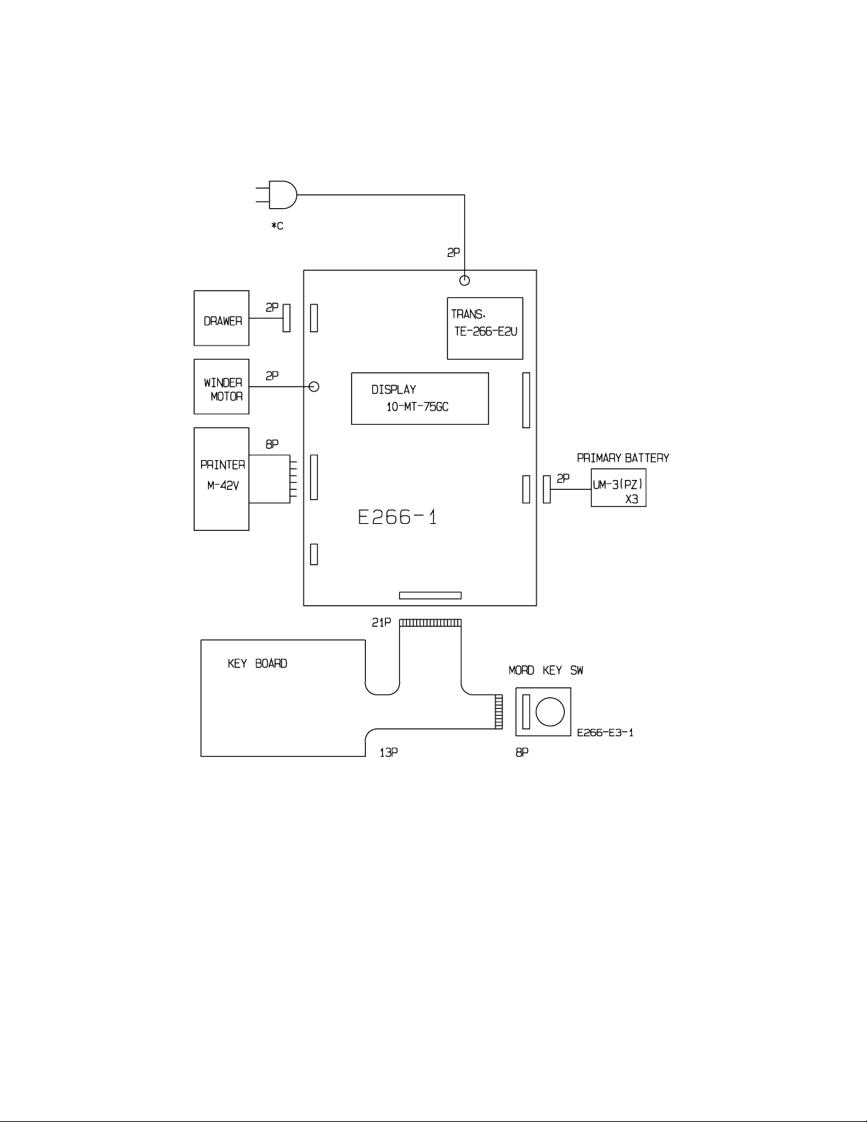
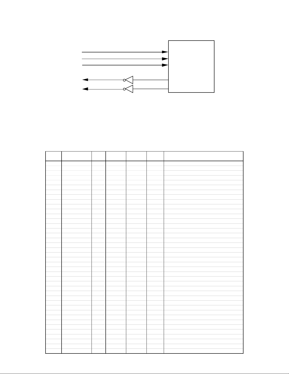
3. BLOCK DIAGRAM
3-1. PCB CONNECTION
— 3 —
Page 6
3-2. BLOCK DIAGRAM
Voltage detection
Buzzer
Winder Motor drive circuit
Printer drive circuit
Drawer drive circuit
Reset IC
DISPLAY
CPU
KEYBOARD
— 4 —
Page 7
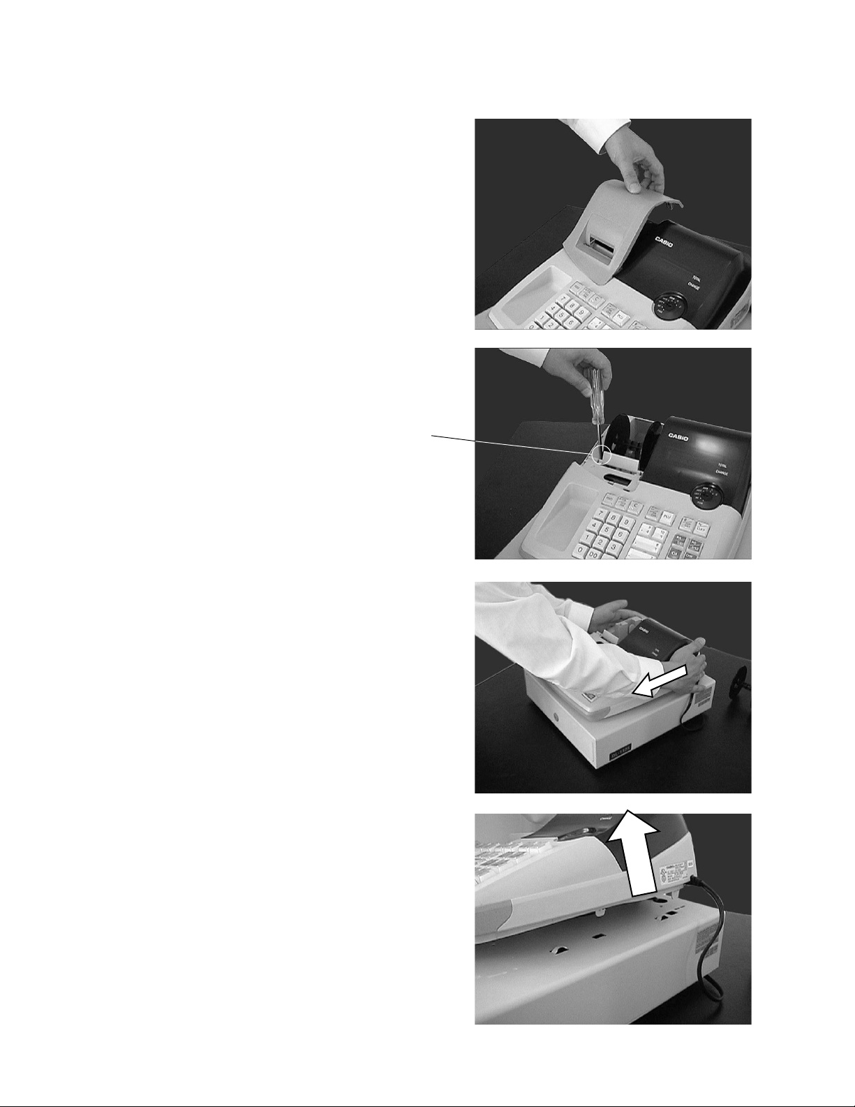
4. DISASSEMBLY
1. Open the printer cover.
2. Remove the screw from the upper case.
Remove the screw.
3. Slide the upper case towards front side.
4. Lift up the upper case.
— 5 —
Page 8
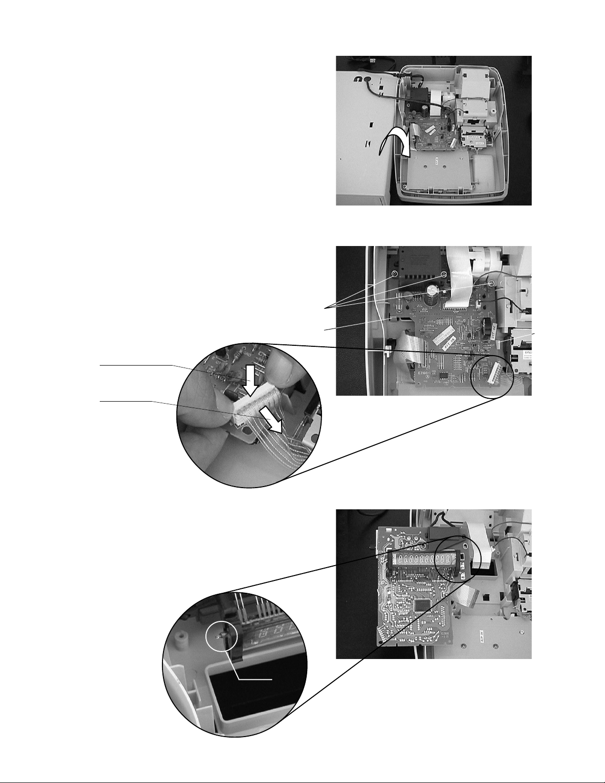
5. Open upper case by lifting it from the left side.
6. Remove all the cables on Main PCB and remove 3
screws.
Remove 3 screws.
Hook
Push the connector.
Pull the wires.
7. Lift up the Main PCB to the right side to avoid the
destruction of Display tube.
Be careful not to damage the point A.
Hook
Point A
— 6 —
Page 9

8. To remove the Printer unit, release the hook of point
B, then lift up the Printer unit.
Point B
— 7 —
Page 10
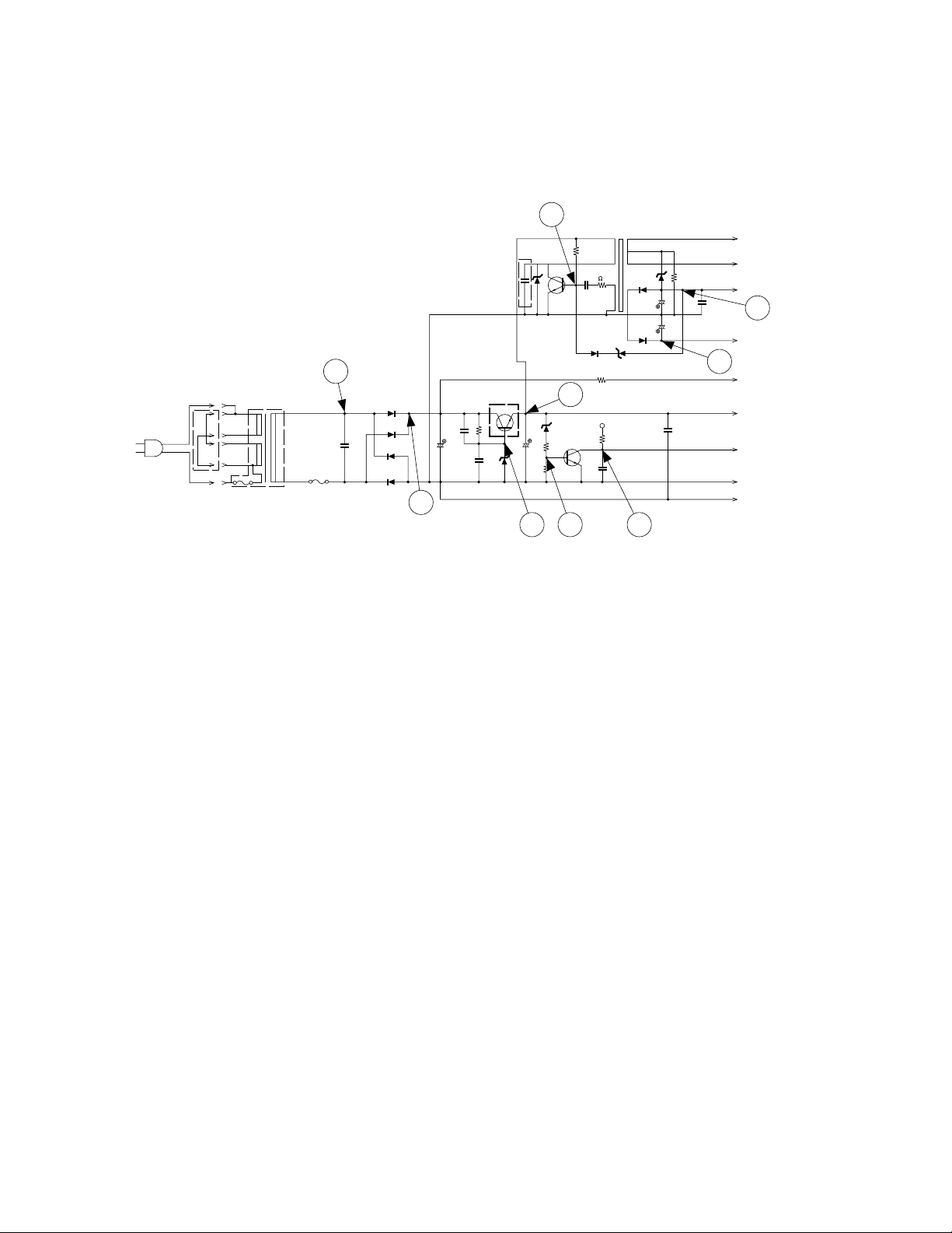
5. CIRCUIT EXPLANATIONS
5-1. Power supply circuit
E412181*1
CN8
*B, *D, *G
T1
TE-266-E2U
6
10
FUSE 1A
F1
A
C1
HE12TKYB103K
1SR35-100A X 4
D1
D2
D3
D4
G
C6
HE50TKYB102K
Q2
ZD2
RD36EB1
2SD1803(T)
WITH HEATSINK
OSH-1625-MP
Q1 2SD2396(K)
ZD5
C3
25V4700uF
C8
R1 1K
HE60TKYB222K
C9
HE60TKYB222K
ZD1
RD6. 8EB1
C7
10V100uF
RD3. 3EB2
150
R17
Q7
560
R16
2SC945
B
D
R4
750
R5
100
C5
HE12TKYB
103K
D6 ZD3
1S2075K RD24EB2
R3
CRH100-FH11J-1R0
C
E
T2
DCS-267
1
3
4
2
5
RD4. 3EB2
D7
7
1S2471
50V4. 7uF
8
10V100µ
D5
9
1S2075K
VDD
R14
470K
C23
ECQ-B1H103-KF
F
ZD4
C11
C4
R6
24K
C17
HE12TKYB103K
H
C28
DSTC50TKYR103K
VF1
VF2
VN
I
VDD
VDW
VP
PWD
GND
GNDP
1. Plug the power cord into AC outlet, secondary voltage (9.65VAC) of the power transformer T1 will
be appears at "A" point.
2. Then, its AC voltage is rectified by the diode bridge and change it to DC voltage. ("B" point)
3. DC voltage appears more than 7V at the corrector of power transistor 2SD2396, and then the power
transistor is turned on.
Then VP is supplied. ("C" point)
4. When the VP voltage becomes more than 3.3V, the transistor 2SD945 is turned on and then PWD
signal becomes GND level. ("F" point)
When the PWD signal becomes GND level, CPU knows no power failure.
5. VP is supplied at the DC DC converter trans T2, the DC DC converter makes display and logic circuit
voltage.
VN ,VF1,VF2 : Display voltage ("I", "J" point )
VDD : Logic circuit voltage ("H" point)
Transistor 2SD1803 is used for oscillating the primary voltage of DC DC converter trans.
— 8 —
Page 11
D
AC IN
GND
A
1A
125V
F1
B
CN8
1
5
6
D1
D2D3D4
C1
B-2
C2
41
VF2
C14
C16
CMK-P2X
E266-1
AC IN
7
HOT
1
R1
B
Q1
B-1
C6
Q2
E
B
D6
R4
10
C3
B-3
C-2
C-3
C15
D-3
F-1
F-2
C17
C-13
C-14
C-12
C26
21
C28
C29
A
C5
T1
D5
C4
R5
T2
20
CN3
D-1
B-4
C-5
C-6
C-7
C-8
C-4
C-3
µPD78042AGF
F-5
IC4
LBI268
A-1
A-2
C30
E
C-15
C-16
C-17
C-18
C-19
C-20
L1
B-5
B-6
B-7
B-9
F-3
F-4
B-15
ZD2
DISP1
Q5
X1
B-10
C-9
X2
R18
E
C7
B
C-10
C18
R20
R19
C8
C10
CN1
1
C11
R6
C-1
ZD3
E-1
D9
B-8
3
IC2
R11
1
R13
B-11
C23
EB
Q7
B-12
C24
B-13
R21
C9
2
E
Q4
ZD4
D7
VN
R10
BR93LC46A
E-2
R12
C21
R16
C25
R22
R23
ZD1
R2
R3
Q3
E
B
R7
C12
D8
B
CN2
R9
R8
2
CN4
C13
C19
IC1
VDD
C22
GND
C26
F-6
C20
S-80728AN
R14
C-23
A-3
A-4
41
VF1
1
D-2
BZ1
Q6
E
B
R15
VP
C-11
ZD5
R17
C-21
C-22
C27
B-14
L2
C31
CN7
8
C
G
21
I
CN5
H
GND
E
1
F
A BC
Power ON
Plug out
9.65 VAC
10.52V
5.76V
000
10.45V
Voltage level is measured at the following condition.
1. Plug the power cord in AC outlet.
2. Mode switch position : REG, display 0.00
3. Put in the memory protection batteries.
4. Plug out : Plug out the power cord , the memory protection batteries in.
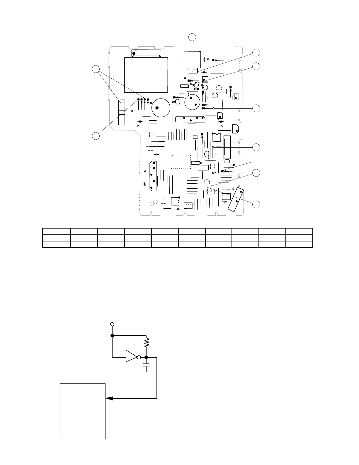
5-2. Reset circuit
VDD
S-80728AN
GND
RESET
Pin No.17
DE
0.78V
00
F
0.12V
4.13V
GH I
Pulse
0
5.07V
4.30V
-23.9V
0
CPU does not work properly when the VDD is unstable.
The reset IC,S-80728AN, is used to know if the VDD is
stable or not. When the VDD voltage becomes 2.8V or
more, the output of the reset IC becomes "H" level.
— 9 —
Page 12
g
p
)
5-3. Printer drive circuit
RP
Pt
PT
CPU
Pin No.44
Pin No.45
Pin No.47
MD
Printer M42
HD
Pin No.62
Pin No.63
When the CPU starts printing, CPU sends MD signal to rotate motor unit.
Then the printer sends back the RP(reset pulse),PT and PT (Timing pulse) to CPU.
After CPU receives RP,PT andPT, CPU knows the position of printin wheel.
And then, CPU sends HD signal to operate the printing magnet when the character selected.
The CPU counts the TP signal to select the character.
5-4. Pin description (CPU uPD78044FGF)
Pin No. Signal In/Out
1 P94/FIP6 Out Pulse -24V L Display digit signal DG7
2 P93/FIP5 Out Pulse -24V L Display digit signal DG6
3 P92/FIP4 Out Pulse -24V L Display digit signal DG5
4 P91/FIP3 Out Pulse -24V L Display digit signal DG4
5 P90/FIP2 Out Pulse -24V L Display digit signal DG3
6 P81/FIP1 Out Pulse -24V L Display digit signal DG2
7 P80/FIP0 Out Pulse -24V L Display digit signal DG1
8 VDD - +5V +5V +5V VDD terminal
9 P27/SCK0 In/Out - - - Not used
10 P26/SO0/SB1 In/Out - - - Not used
11 P25/SI0/SB0 In/Out - - - Not used
12 P24/BUSY In/Out - - - Not used
13 P23/STB Out H H H Strobe signal for AVREF
14 P22/SCK1 Out L H H SK signal for EEPROM
15 P21/SO1 Out L H H DI signal for EEPROM
16 P20/SI1 In H H H DO signal for EEPROM
17 RESET In H H H Reset signal
18 P74 Out H H L Drawer open signal
19 P73 Out L H H Common signal for PAD condition
20 AVSS - GND GND GND GND for AD converter
21 P17/ANI7 In GND GND GND GND
22 P16/ANI6 In GND GND GND GND
23 P15/ANI5 Out L L H Chip enable signal for EEPROM
24 P14/ANI4 In GND GND GND GND
25 P13/ANI3 In GND GND GND GND
26 P12/ANI2 In GND GND GND GND
27 P11/ANI1 In GND GND GND GND
28 P10/ANI0 In H H H Low battery detection terminal
2 9 AVDD - H H H Power for AD converter
30 AVREF In L L L Voltage for AD converter (VDD)
31 XT1 In Pulse Pulse Pulse Sub system clock
32 XT2 - Pulse Pulse Pulse Sub system clock
33 VSS - GND GND GND GND
34 X1 In Pulse L L Main system clock
35 X2 - Pulse H H Main system clock
36 P37 In L L L Mode switch position (OFF)
37 P36/BUZ Out L L L Buzzer signal
38 P35/PCL In L L L Mode switch position (Z)
39 P34/T12 In L L L Mode switch position (X)
40 P33/T11 In L L L Mode switch
Mode SW
REG
Mode SW
OFF
AC cord
Plu
off
Description
osition (CAL
— 10 —
Page 13

Pin No. Signal In/Out
g
play
41 P32/TO2 In H L L Mode switch position (REG)
42 P31/TO1 In L L L Mode switch position (RF)
43 P30/TO0 In L L L Mode switch position (PRG)
44 P03/INTP3/CI0 In H L L Reset pulse RP from printer
45 P02/INTP2 In H Pulse L Sub timimg pulse Pt from printer
46 P01/INTP1 In L L H Power down signal PWD
4 7 P00/INTP0/TI0 In H L L Main timing pulse PT from printer
48 IC - GND GND GND GND
49 P72 In H H H TAX PAD signal for Japan
5 0 P 71 In - - - PAD2 condition
5 1 P7 0 In L H H PAD1 condition
5 2 VDD - +5V +5V +5V Power (+5V)
53 P127/FIP33 In L L L Key input signal KI7
54 P126/FIP32 In L L L Key input signal KI6
55 P125/FIP31 In L L L Key input signal KI5
56 P124/FIP30 In L L L Key input signal KI4
57 P123/FIP29 In L L L Key input signal KI3
58 P122/FIP28 In L L L Key input signal KI2
59 P121/FIP27 In L L L Key input signal KI1
60 P120/FIP26 In L L L Key input signal KI0
61 P117/FIP25 Out L L L Winder motor drive signal WMO
62 P116/FIP24 Out L L L Printer moter drive signal PMO
63 P115/FIP23 Out L L L Head drive signal for printer PHD
64 P114/FIP22 Out Pulse L L Key common signal KC3
65 P113/FIP21 Out Pulse L L Key common signal KC2
66 P112/FIP20 Out Pulse L L Key common signal KC1
67 P111/FIP19 Out Pulse L L Key common signal KC0
68 P110/FIP18 Out H H H Not used (+5V)
69 P107/FIP17 Out Pulse -24V L Display segment signal Sdp (Decimal point)
70 P106/FIP16 Out Pulse -24V L Display segment signal Sg
71 VLOAD - -24V -24V L Display voltage VN
72 P105/FIP15 Out Pulse -24V L Display segment signal Sf
73 P104/FIP14 Out Pulse -24V L Display segment signal Se
74 P103/FIP13 Out Pulse -24V L Display segment signal Sd
75 P102/FIP12 Out Pulse -24V L Display segment signal Sc
76 P101/FIP11 Out Pulse -24V L Display segment signal Sb
77 P100/FIP10 Out Pulse -24V L Display segment signal Sa
78 P97/FIP9 Out H Pulse L Mode switch common signal
79 P96/FIP8 Out Pulse -24V L Display digit signal DG9
80 P95/FIP7 Out Pulse -24V L Dis
Mode SW
REG
Mode SW
OFF
AC cord
Plu
off
Description
digit signal DG8
Note : Above data is measured under following condition.
Mode SW REG : AC cord plug in the AC outlet, Memory protection batteries in,
Mode SW position : REG
Mode SW OFF : AC cord plug in the AC outlet, Memory protection batteries in,
Mode SW position : OFF
AC cord plug off : AC cord plug out the AC outlet, memory protection batteries in,
Mode SW position : OFF
— 11 —
Page 14

6 DIAGNOSTIC OPERATIONS
6-1. To start the diagnostic operation
1. Make MAC operation.
2. Turn the mode switch to PGM position.
3. Input "99999999" and press "SUB TOTAL" key.
Note : Do not issue the receipt under REG / RF / X / Z mode before execute the diagnostic.
If the machine issued a receipt, the diagnostic does not start.
Print ing Layout
0 0 - 0 0 - 0 0
0 0 - 0 0 # 0 0 0 2
- d1d2d3d4 - - d5d6d7
d1d2d3d4 : Version No.
d5 : PAD condition
0 : Japan
1 : Export (ADD2)
2 : US / Canada
3 : Export (ADD3)
4 : Export (ADD1)
d6 :
0 : Non taxable (Japan)
1 : Taxable (Japan)
- : Export version
d7:
0 : 118ER (Japan)
1 : 108ER (Japan)
- : Export version
Receipt sample
0 0 - 0 0 - 0 0
0 0 - 0 0 # 0 0 0 2
- 2 8 6 2 - - 1 - -
6-2. Check items
The following test can be checked in the test mode.
1. Key code check
2. Switch check
3. Individual function check
— 12 —
Page 15

6-3. Operations
1. Key code check (Hard key code)
When pressing a key, the machine displays the following key code.
Key code table
FEED 029 C 021 017028 023
789
456
123
0 011 012
027 022
026
025
024
Display
022
022 : Hard key code
2. Switch check
Press " C " button, the switch condition is appered on a display.
020 016
019 015
018 014
013
Always 0
No display
No display
PAD1 condition
EEPROM mounted : 1
PAD2 condition
Open : 1
Short : 0 (Export version)
Non taxable PAD
Short : 1
Open : 0 (export version)
FEED button
OFF : 0
ON : 1
Mode key condition
PRG : 1 X : 5
RF : 2 Z : 6
REG : 3 OFF : 8
CAL : 4 Others: 0
— 13 —
No EEPROM : 0
Page 16

3. Individual test
After finishing each test, the machine issues the following receipt.
US
d1 #
d1 : Test command No.
Sample receipt
#1
1234567890ST#
3-1. General test
Press "1" key and "SUB TOTAL" key.
The machine executes the following tests.
All segment display
Set time and date
Date : 31st Dec. '94 Time : 23:59
Open drawer
Print check
US
Issue a test receipt
Display test data
123456789012ST#
1234567
3-2. Mode selection (Receipt / Journal)
Press "2" key and "SUB TOTAL" key.
Change the mode to "Journal" from "Receipt".
8
— 14 —
Page 17

3-3. Battery voltage check
Press "7" key and "SUB TOTAL" key.
Display the voltage level of memroy protection battery.
To escape this test, turn the mode switch to "OFF".
VCC=5.35V(Standard)
5 35
3-4. Print test
Press "8" key and "SUB TOTAL" key.
The machine prints all chatacter.
Receipt sample
# 8
0 0 0 0 0 0 0 0 0 0 CA Z
1 1 1 1 1 1 1 1 1 1 CH 1
2 2 2 2 2 2 2 2 2 2 RA 2
3 3 3 3 3 3 3 3 3 3 PO 3
4 4 4 4 4 4 4 4 4 4 NT 4
5 5 5 5 5 5 5 5 5 5 STCK
6 6 6 6 6 6 6 6 6 6 AT +
7 7 7 7 7 7 7 7 7 7 CG 8 8 8 8 8 8 8 8 8 8 TX X
9 9 9 9 9 9 9 9 9 9 RF@
- - - - - - - - - , , , , , , , , , , * #
• • • • • • • • • •%NS
# # # # # # # # # # VDTA
3-5. Time test
Voltage level
Note : US version is printed out
14 characters.
Press "9" key and "SUB TOTAL" key.
Display the time.
To escape this test, press "C" key.
4. To escape the diagnostic operation
Exexute the MAC operation (Memory All Clear).
Note : Make sure to remove the memory protection batteries.
— 15 —
2 3- 59 12
Page 18

7. ERROR CODE LIST
7-1. Operation error code
Error codes appear on display whenever you make a mistake during operation.
Error Code
E01
E94
Press
Meaning
Changing modes without completing transaction.
Printer paper is jammed.
Return key to where is stops buzzing and
AMT
press
CA
TEND
=
Remove jammed paper. Turn Mode
Action
.
switch to OFF then turn to ON, or Turn
power OFF and then turn power ON.
C
key and check the appropriate section of this manual for the operation you want to perform.
C/AC
— 16 —
Page 19

8. IC DATA
8-1. LB1268
Equivalent circuit
1
4
8-2. S-80728AN-Z
8
5
1 OUT
2 V
DD
3 V
SS
270
TR1
30k 30k
6.8k
2k
1
IN1
OUT1
8
01
TR2 TR4 TR6
6.8k 3.4 1k
2
IN2
OUT2
7
D2270
TR3
2k
IN3
V
–
TR5
15k
3
DD
RA
+
OUT3
6
5
VCC
D3135
4
GND
OUT
123
Bottom view
V
V
SS
— 17 —
REF
RB
1
RC
Page 20

9. PCB LAYOUT
125V
AC IN
1
GND
5
C1
1A
F1
CN8
6
D1
D2D3D4
B-2
C2
41
VF2
B-3
C-2
C14
C15
F-2
C16
CMK-P2X
E266-1
E266
-1 A
A
F-1
C17
21
D-3
AC IN
7
HOT
1
R1
B
Q1
B-1
C6
C-7
C-8
L1
CN3
ZD2
B
D6
R4
T2
B-4
DISP1
Q5
E
C-9
C18
X1
X2
B-10
C-15
C-16
C-17
C-18
C-19
C-20
R19
R18
Q2
E
R5
20
D-1
C-5
B-6
B-7
C-4
µPD78042AGF
F-4
F-5
C30
C5
D5
C4
C-3
IC4
LBI268
A-1
A-2
C-6
10
T1
C3
C-3
B-5
C-13
C-14
B-9
C-12
F-3
C26
C28
C29
B-15
E
C10
CN1
1
C7
ZD3
B
D9
B-8
C-10
IC2
R11
B-11
EB
B-12
B-13
R20
C11
R6
C8
C-1
E-1
3
1
R13
C23
Q7
C24
R21
C9
R2
2
E
R7
E
Q4
ZD4
D7
VN
R10
C13
BR93LC46A
IC1
VDD
E-2
R12
C21
GND
R16
C25
C26
R22
R23
R3
ZD1
Q3
B
R8
2
C19
C22
F-6
B
R9
VF1
1
D-2
C20
S-80728AN
E
R14
C-23
A-3
A-4
C31
R17
B-14
C12
CN4
C-21
C-22
L2
R15
C-11
ZD5
CN7
21
D8
CN2
41
CN5
BZ1
Q6
B
VP
1
C27
8
— 18 —
Page 21

10. CIRCUIT DIAGRAMS
MODEL : PCR-260B (EX-268)
CONTENTS
1. LOCATION OF PRINTED CIRCUIT BOARD .................................................................. 20
2. MAIN PCB CIRCUIT
2-1. MAIN PCB CIRCUIT (1/3) ........................................................................................ 21
2-2. MAIN PCB CIRCUIT (2/3) ........................................................................................ 22
2-3. MAIN PCB CIRCUIT (3/3) ........................................................................................ 23
3. KEYBOARD ..................................................................................................................... 24
— 19 —
Page 22

BCDEFGHI JKA
1
2
3
4
— 20 —
5
1
2
3
4
5
6
7
8
Description: Board No. Drawing No.
LOCATION OF PRINTED
CIRCUIT BOARDS
6
7
8
BCDEFGHI JKA
Page 23

BCDEFGHI JKA
Note: Not used Q5.
Note: Not used BR93LC46A.
— 21 —
1
2
3
4
5
1
2
3
4
5
6
7
8
Description: Board No. Drawing No.
MAIN PCB
BCDEFGHI JKA
E268-1 (1/3)
E240713
6
7
8
Page 24

BCDEFGHI JKA
— 22 —
1
2
3
4
5
1
2
3
4
5
6
7
8
Description: Board No. Drawing No.
MAIN PCB
BCDEFGHI JKA
E268-1 (2/3)
E341104
6
7
8
Page 25

BCDEFGHI JKA
Location Specification
Location Specification
HEATSINK
Power Cord
1
2
3
4
— 23 —
5
1
2
3
4
5
6
7
8
6
7
8
Description: Board No. Drawing No.
MAIN PCB
E268-1 (3/3)
E240714
BCDEFGHI JKA
Page 26

BCDEFGHI JKA
— 24 —
1
2
3
4
5
1
2
3
4
5
6
7
8
Description: Board No. Drawing No.
KEYBOARD
BCDEFGHI JKA
E268-1E4
E341101
6
7
8
Page 27

11. PARTS LIST
MODEL : PCR-260B (EX-268EC)
CONTENTS
Exploded view................................................................................................... 26
1. Main PCB block..........................................................................................28
2. Button block ............................................................................................... 29
3. Power supply block .................................................................................... 30
4. Upper case block ....................................................................................... 30
5. Printer block ............................................................................................... 30
6. Others ........................................................................................................ 30
7. Cash drawer (DL-1325)..............................................................................31
8. Printer Unit. M-42V.....................................................................................33
Notes:
1. Prices and specifications are subject to change without notice.
2. As for order / supply of spare parts, refer to the "GUIDEBOOK for Spare Parts Supply", a separate
publication.
3. The numbers in item column correspond to the same numbers in drawing.
4. MARKS:
Q: Quantity used per unit
R: Rank
A: Essential
B: Stock recommended
C: Less recommended
X: No stock recommended
— 25 —
Page 28

36
41
32
40
29
39
34
4
48
47
50
49
46
51
38
33
3
2
35
45
E266-1
PCB
43
30
37
42
A
31
1
— 26 —
B
44
Drawer
Page 29

Keyboard Block
33
13
14
18
11
6
28
23
24
12
10
9
6
8
3
5
7
4
7
.
2
00
1
0
16
17
8
5
9
15
20
19
21
22
25
B
A
26
27
— 27 —
Page 30

N Item Code No. Parts Name Specification Q 't y Price code R a nk
1. Main PCB block
N 1 1011 1100 PCB ASSY /E268-1 E140376*14 1 A
F1 3631 0330 FUSE 237001 1 AD A
IC2 2120 7393 IC/RESET S-80728AN-Z 1 AD A
IC3 1002 4618 LSI UPD78044FGF177-3B9 1 BR A
IC4 2120 6253 IC/MOS LB1268 1 AG A
X1 2520 3445 OSCILLATOR/CRYSTAL C-002RX(M90-76) 1 AD A
X2 2801 8932 LOCK/CERAMIC CST4.19MGW 1 AC A
D1-4,8 2315 2682 DIODE 1SR35-100A-T-82 5 AA B
D5,6,9 2315 2689 DIODE 1S2075K-TD 3 AA B
D7 1001 9404 DIODE 1S2471T-77-T 1 AA B
Q1 2250 1036 TRANSISTOR 2SD2396(K) 1 AE B
Q2 2250 1022 TRANSISTOR 2SD1803(T) 1 AF B
Q3 2250 1029 TRANSISTOR 2SD1961(S) 1 AC B
Q4 2200 9141 TRANSISTOR 2SA933(K,P,Q,R)T93 1 AA B
Q6 2250 0847 TRANSISTOR/DIGITAL DTC143ZS-TP 1 AA B
Q7 2220 2456 TRANSISTOR 2SC945(K,P,Q,R)-T 1 AA B
ZD1 2315 2675 DIODE/ZENER RD6.8EB1-T1 1 AA B
ZD2 2315 2661 DIODE/ZENER RD36EB1-T1 1 AA B
ZD3 2315 2766 DIODE/ZENER RD24EB2-T1 1 AA B
ZD4 2315 2759 DIODE/ZENER RD4.3EB2-T1 1 AA B
ZD5 2315 2654 DIODE/ZENER RD3.3EB2-T1 1 AA B
N C19 1008 0945 DIODE/ZENER RD6.2ESAB1 1 B
2 2408 8219 TUBE/DISPLAY 10-MT-75GC 1 BJ B
3 1001 8619 STAND/L DISPLAY E341001-1 1 AC C
4 1001 8618 STAND/R DISPLAY E341002-1 1 AC C
BZ1 3240 2089 BUZZER PKM22EPT-2001 1 AE C
C11 2807 2735 CAPACITOR/ELECTROLYTIC RE2-50V4R7M-T2 1 AA C
C14,15 2818 0446 CAPACITOR/CERAMIC RT-HE40TKYB101K-T 2 AA C
C3 2807 2658 CAPACITOR/ELECTROLYTIC RE3-25V472M 1 AL C
C4,7 2807 2315 CAPACITOR/ELECTROLYTIC RE3-10V101M-T2 2 AA C
CN1 6246 2780 C ONNECTOR SUB ASSSY E311971*1 1 AE C
CN2 3500 3371 CONNECTOR IL-G-2P-S3T2-E 1 AA C
CN4 3510 3465 CONNECTOR 5267-02A 1 AA C
CN6 3540 4759 CONNECTOR IMSA-9604S-21C 1 AC C
CN7 3500 1077 CONNECTOR 52011-0810 1 AC C
CN8 6246 2830 C ONNECTOR SUB ASSSY E412181*1 1 AP C
C1,5,17 CAPACITOR/CERAMIC RT-HE12TKYB103K-T 3 X
C10,12 CAPACITOR/CERAMIC RT-HE40TKYB221K-T 2 X
C2,16,19,28,29,30 CAPACITOR/CHIP RT-DSTC50TKYR103K 4 X
C20,23,31 CAPACITOR/CHIP ECQ-B1H103-KF 3 X
C21,22 CAPACITOR/CERAMIC RT-HE40TKCH120J-T 2 X
C8,9,13,18,24-27 CAPACITOR/CERAMIC RT-HE60TKYB222K-T 7 X
R1,15,21-23 RESISTOR CR-25-1KOHM-J-T 5 X
R10,11,18-20 RESISTOR CR-25-100KOHM-J-T 5 X
R13 RESISTOR CR-25-330KOHM-J-T 1 X
R14 RESISTOR CR-25-470KOHM-J-T 1 X
R16 RESISTOR CR-25-560OHM-J-T 1 X
R17 RESISTOR CR-25-150OHM-J-T 1 X
R2 RESISTOR CRH100-FH11J-10R 1 X
R3 RESISTOR CRH100-FH11J-1R0 1 X
R4 RESISTOR CR-25-750OHM-J-T 1 X
R5 RESISTOR CR-25-100OHM-J-T 1 X
R6 RESISTOR CR-25-24KOHM-J-T 1 X
R7 RESISTOR CR-25-75OHM-J-T 1 X
R8 RESISTOR CR-25-2.2KOHM-J-T 1 X
R9 RESISTOR CR-25-4.7KOHM-J-T 1 X
SCREW 3X12 ZMC-3... 3 X
— 28 —
Page 31

N Item Code No. Parts Name Specification Q 't y Price code R a nk
AMT
CA
2. Button block
5 6221 3988 CAP/L E210964-1 4 AB C
6 6221 4025 CAP/S E311103-1 15 AA C
7 6245 7250 BUTTON/1 E311792-1 1 AB C
8 6245 7260 BUTTON/2 E311792-2 1 AB C
9 6245 7270 BUTTON/3 E311792-3 1 AB C
10 6245 7280 BUTTON/4 E311792-4 1 AB C
11 6245 7290 BUTTON/6 E311792-5 1 AB C
12 6245 7300 BUTTON/7 E311792-6 1 AB C
13 6245 7310 BUTTON/8 E311792-7 1 AB C
14 6245 7320 BUTTON/9 E311792-8 1 AB C
15 6245 7330 BUTTON/0 E311792-9 1 AB C
16 6245 7340 BUTTON/. E311792-10 1 AB C
17 6245 7350 BUTTON/ 00 E311792-11 1 AB C
18 6245 7360 BUTTON/5 E311116-4 1 AB C
19 6246 7768 KEY TOP/L E210963A-4 4 AD B
20 6246 7810 KEY TOP/S E311101A-4 27 AA B
21 6247 3830 SPRING/COIL E411104A-1 4 AA B
22 6248 0990 RUBBER/CONTACT E411877A-1 31 AA B
23 6247 3837 SPRING/COIL E411104A-2 4 AA B
24 1001 8612 SHEET/COMMON E341006-1 1 AH B
25 1001 8611 SPACER E341005-1 1 AB C
26 1001 8610 FP C E341004-1 1 AR B
27 1001 8613 CHASSIS/KEY BOARD E341007-1 1 AE C
28 1001 8609 FLAME/KEYBOARD E240664-1 1 AT C
FEED 1002 7139 PLATE/S E240685-1 1 AA C
AC C 1002 7140 PLATE/S E240685-2 1 AA C
X / FOR
/ DATE TIME
ERR.
-/ 1002 7142 PLATE/S E240685-4 1 AA C
CORR
AA C1002 7141 PLATE/S E240685-3 1
PLU 1002 7143 PLATE/S E240685-5 1 AA C
DEPT
# / 1002 7144 PLATE/S E240685-6 1 AA C
SHIFT
% / CLK# 1002 7145 PLATE/S E240685-7 1 AA C
RA 1002 7146 PLATE/S E240685-8 1 AA C
T/S1
PO 1002 7147 PLATE/S E240685-9 1 AA C
T/S2
CH 1002 7148 PLATE/S E240685-10 1 AA C
CHK / NS 1002 7149 PLATE/S E240685-11 1 AA C
SUB TOTAL 1002 7150 PLATE/S E240685-12 1 AA C
MD / S T 1002 7151 PLATE/S E240685-13 1 AA C
9
+ 4
10
5
8
x 3
7
- 2
6
+ 1
1002 7152 PLATE/S E240685-14 1 AA C
1002 7153 PLATE/S E240685-15 1 AA C
1002 7154 PLATE/L E341057-1 1 AA C
1002 7155 PLATE/L E341057-2 1 AA C
1002 7156 PLATE/L E341057-3 1 AA C
TEND
/
-
1002 7157 PLATE/L E341057-4 1 AA C
SCREW 3X8 ZMC-3..... 2 X
— 29 —
Page 32

N Item Code No. Parts Name Specification Q 't y Price code R a nk
3. Power supply block
29 3701 0228 CORD/POWER ME301S 1 AW C
30 3000 7098 TRANSFORMER TE-266-E2U 1 BP A
31 6246 2850 CASE/TRANSFORMER E311870-1 1 AL C
4. Upper case block
N 32 1011 1101 COVER/DISPLAY E140370-12 1 C
N 33 1009 3974 CASE/UPPER E140368-9 1 C
34 1001 8621 COVER/BATTERY E341000-1 1 AH C
N 35 1004 4455 COVER/COSMETIC E240663-3 1 C
SCREW 3X8 ZMC-3..... 5 X
SCREW 3X12 ZMC-3... 3 X
5. Printer block
N 36 1004 4454 COVER/PRINTER E268 E140369-3 1 AV C
37 1090 5329 PRINTER UNIT M-42V-001-060MA 1 CB A
38 6231 3668 CUTTER/PAPER E42592A-1 1 AB C
39 6246 1830 PULLEY/WIND E266 E311860-1 1 AJ C
40 6221 4029 SPOOL/PAPER HOLD E277 E411393-1 1 AE C
6. Others
N 41 1010 4982 KEY SET SUB ASSY RJE500074*3 1 B
42 3200 3672 MOTOR MXN-13FB12F 1 AV B
43 6246 1820 CASE/MOTOR E311858-1 1 AF C
6231 6837 RUBBER/WINDER E410716A-1 1 AB C
44 1003 1022 METAL/EARTH E441146-1 1 AC C
45 6192 4970 SWITCH ASSY/MODE KEY E311944*1 1 BL B
46 6000 6091 SPRING/BATTERY G67 A43656-1 1 AA C
47 6322 4499 SPRING/BATTERY A-G55 A42606-1 1 AA C
48 6001 0862 SPRING/BATTERY B-1G513 P408-1 1 AB C
49 6001 0871 SPRING/BATTERY B-2G513 P409-1 1 AA C
50 6221 2292 WIRE SUB ASSY E411266*1 1 AB C
51 6221 2284 CONNECTOR SUB ASSY E411265*1 1 AC C
WASHER 4 ZMC-3 3 X
SCREW 3X8 ZMC-3 3 X
SCREW 3X8 ZMC-3 1 X
SCREW 3X8 NI 1 X
CUSHION E248 E441127-1 1 X
SCREW 4X85 ZMC-3 1 X
WASHER 4X9X0.8 ZMC-3 1 X
SCREW 4X8 ZMC-3 2 X
— 30 —
Page 33

7. Cash drawer (DL-1325)
25
26
24
11
19
17
18
16
23
22
× 2
20
× 4
5
× 4
4
× 3
12
2
8
14
× 2
3
15
× 2
7
× 2
6
21
× 5
1
10
13
× 4
9
— 31 —
Page 34

N Item Code No. Parts Name Specification Q ty Price Code Rank
N 1 1002 2673 DRAWER ASSY
N 2 1002 2665 CASE/COIN E240644-1 1 B
3 6246 6571 PLATE /BILL HOLDER FIXING E311873-1 1 AS C
4 6248 1217 HOLDER/BILL E340725-1 4 AA A
5 6246 5220 SPRING/BILL HOLDER E412160-1 4 AB A
SCREW 3X8 ZMC-3 3 X
6 5500 0878 ROLLER/DELIN DR-19B2 2 AP A
7 5150 1643 NUT 6... 2 AA X
8 5150 1648 RIVET/FLAT D5X26 1 AA X
9 5580 1452 CS RING CSTW-5 1 AA X
10 6246 4960 CYLINDER LOCK ASSY E311950*1 1 AT C
11 6246 5000 DRAWER KEY SUB ASSY E412062*1 1 AG C
12 6246 6585 PLATE/ PARTITION E340010-5 3 AC B
N 13 1002 2666 PLATE/COIN PARTITION E340966-1 4 B
14 6248 1222 CASE/BOTTOM E110360B-1 1 BV X
15 5500 0878 ROLLER/DELIN DR-19B2 2 AP A
16 5150 1643 NUT 6... 2 AA X
17 6246 4940 LEVER/HOOK E311876-1 1 AF B
18 6246 5020 SHAFT/HOOK LEVER E412071-1 1 AB X
SCREW 3X5 ZMC-3 2 X
19 5580 1461 SPRING/LOCK ZD03441-A 1 AA B
20 6246 6522 SPRING/PUSH E412137-1 1 AA B
21 6246 6529 RUBBER/FOOT E412136-1 5 AD X
SCREW 4X14 ZMC-3 1 X
N 22 6246 1240 REINFORCEMENT E412172-1 1 X
23 6246 6557 CUSHION E440023-1 1 AD C
N 24 1002 9529 SOLENOID ASSY TDS-06U-332T-140 1 A
25 1002 9558 TOP COVER/E268 E240692-1 1 CF X
SCREW 3X8 ZMC-3 6 X
N 26 1002 9530 LABEL/DRAWER E341010-4 1 X
E240689*1 1 C
— 32 —
Page 35

103
126
127
128
124
129
144
110
130
122
151
152
102
134
138
140
120
142
111
123
113
112
114
118
109
131
115
107
108
101
143
101
135
106
133
139
137
116
Ink roll ass'y
119
101
145
117
132
125
105
*The exploded diagram is made based on the standard specification of our company.
When the part or unit indifferent from your specification is shown in the
diagram, please disregard it.
8. Printer Unit. M-42V
— 33 —
Page 36

N Item Code No. Parts Name Specification Q M
101 1903 0201 Rubber fitting F801001050 3 15 X
102 1908 7661 Motor F818051010 1 600 A
103 1908 7662 Motor gear F817051010 1 25 C
105 1908 7663 Cup screw M2x2.9 B040352118 2 12 X
106 1908 7664 Paper feed drive gear ass'y F815101000 1 140 C
107 1908 7665 Detector ass'y F815151000 1 180 A
108 1903 2244 Detection wheel F808152010 1 870 A
109 1903 1976 Print wheel shaft F808202010 1 100 X
110 1903 0219 Print wheel spring F801202020 1 23 C
111 1903 0791 Retaining ring TYPE-E(1.5) B150300311 1 3 X
112 1906 8909 Print wheel (for USA, Canada) M817001060 1 320 A
113 1906 8902 Hammer transmission lever ass'y F815210000 1 5 75 C
114 1906 8903 Carriage F817208010 1 5 75 C
115 1906 8907 Hammer (for except Japan) F809201020 1 103 C
116 1903 2246 Hammer return spring F808201020 1 18 C
117 1908 7676 Print cam F817201020 1 63 C
118 1903 2298 Carriage spring F812201020 1 5 75 C
119 1908 7670 Ink roll spring F817201010 1 25 C
120 1908 7318 Selective pawl spring F818209010 1 10 50 C
122 1909 1858 Paper feeding transmission gear F815212010 1 38 C
123 1903 0220 Paper feeding ratchet wheel F801202030 1 10 23 C
124 1906 8904 Print change over cam F815215010 1 5 50 C
125 1903 0234 Planet gear F801206020 2 53 C
126 1903 0235 Selecting drive gear F801206030 1 38 C
127 1908 7674 Reduction gear F817203010 1 25 C
128 1903 0792 Retaining ring TYPE-E(1.2) B150300212 1 3 X
129 1906 8905 Coil selective gear ass'y F818230000 1 200 C
130 1903 0791 Retaining ring TYPE-E(1.5) B150300311 1 3 X
131 1903 1968 Positioning shaft F806206010 1 40 X
132 1903 2280 Positioning plate F808205010 1 100 X
133 1903 0293 Selecting ratchet F804204010 1 53 X
134 1903 0264 Trigger lever spring F803204020 1 10 24 C
135 1908 7675 Return lever F815207010 1 38 C
137 1903 0230 Trigger plate F801205100 1 53 C
138 1903 0231 Trigger plate spring F801205110 1 10 15 C
139 1903 2293 Return lever spring F810205020 1 18 C
140 1903 0226 Trigger lever F801205060 1 38 C
141 1903 1972 Platen shaft F806207010 1 100 X
142 1903 0241 Carriage feeding gear F801211020 1 38 C
143 1908 7321 Platen ass'y F818251000 1 20 290 X
144 1906 8910 Jumper wire F818601010 1 10 130 X
145 1906 8906 Plain washer G F817210010 1 25 X
151 1908 7672 Selective pawl spring holder F818202020 1 25 X
152 1903 0674 Cup screw 2x3.5 B040351111 1 6 X
FOB Japan
N.R.Yen
Unit Price
R
— 34 —
Page 37

CASIO TECHNO CO.,LTD.
Overseas Service Division
6-2, Hon-machi 1-Chome
Shibuya-ku, Tokyo 151-8543, Japan
 Loading...