

Page 1
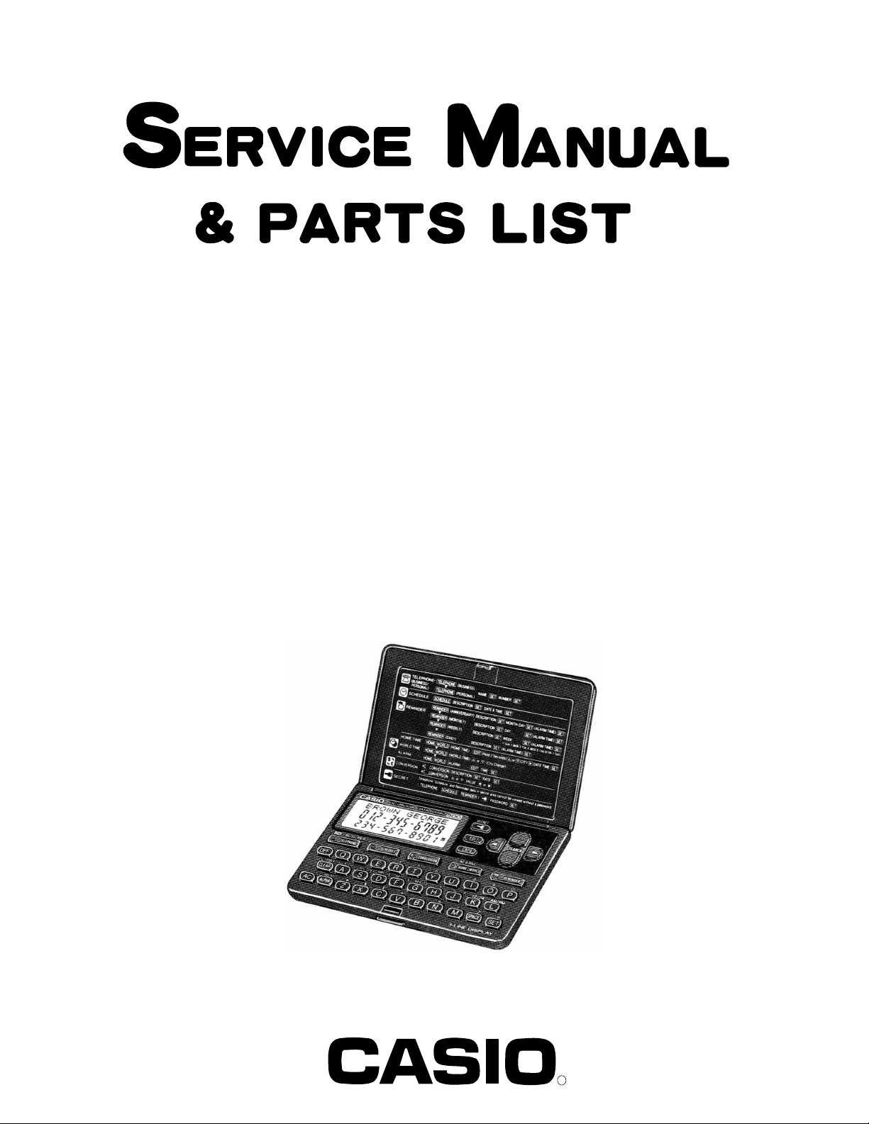
DC-7500A
INDEX
JUL. 1994
(without price)
DC-7500A
R
Page 2

SPECIFICATIONS
Display: Liquid crystal display
Power supply: Two lithium batteries (CR2025) ......... Main and Back-up
Power consumption: 0.004 W
Battery life: Main battery: approximately 2 years (1hour use per day)
Back-up battery: approximately 1 year after the "LOW BATTERY"
message appears on the display
Auto power off: Approximately 6 minutes after last key operation
Ambient temperature range: 0°C ~ 40°C (32°F ~ 104°F)
Dimensions: 11.9 (H) × 119 (W) × 77.5 (D) mm ..... Folded
(1/2" (H) × 4 5/8" (W) × 3" (D))
8.3 (H) × 119 (W) × 151 (D) mm ........ Unfolded
(3/8" (H) × 4 5/8" (W) × 6" (D))
Weight: 84.2 g (3 oz) (including batteries)
— 1 —
Page 3
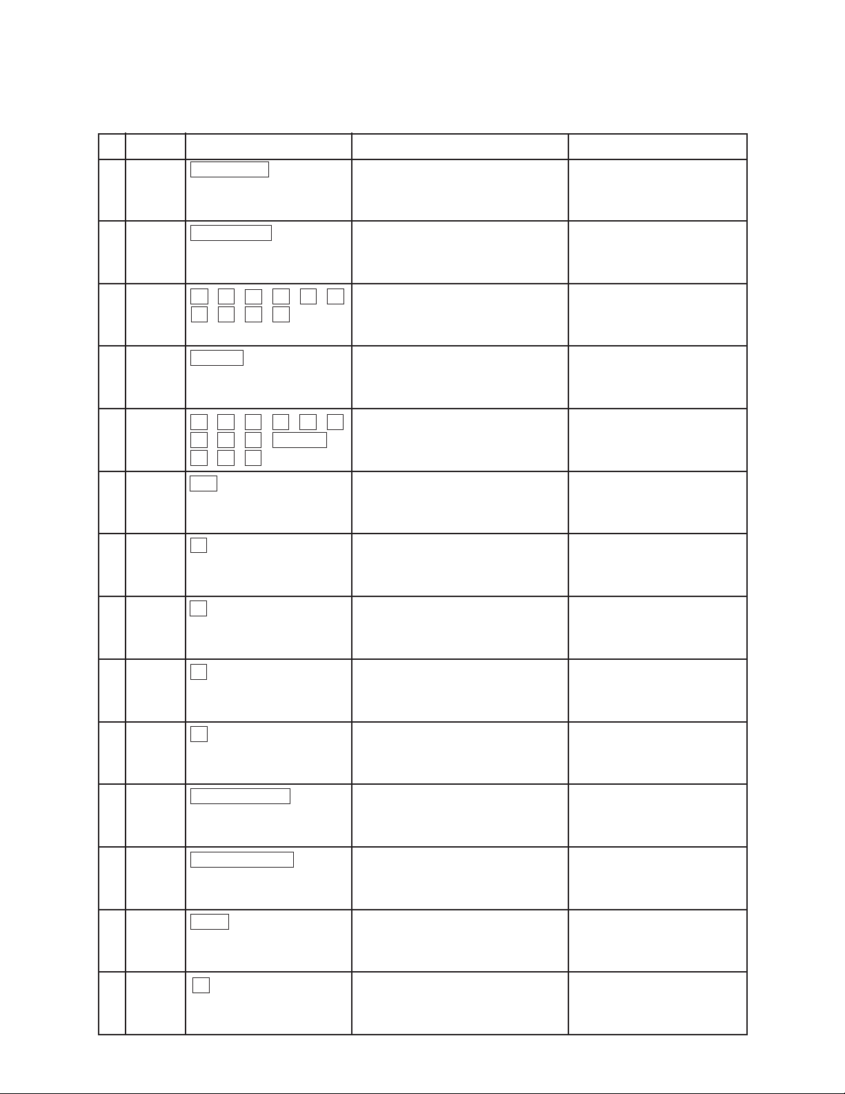
OPERATION CHECK
Note: Before you do this operation, save the data to another unit.
No. MODE DISPLAYKEY NOTE
TELEPHON
1
NAME?
A
☎
SCHEDULE
2
Q WER YT
3
4
5
6
7
U
CLEAR
ASDF HG
J
Z
AC
V
LK
CX
POI
ALPHA
SCHEDULE?
A
QWERTYUIOP_
A
SCHEDULE?
A
ASDFGHJKL¥$£
°
°
°
°
0.
+
0.
B
8
–
0.
9
10
11
12
13
14
N
M
CONVERSION
HOME/WORLD
EDIT
g
×
0.
÷
0.
CONVERSION?
SAT
1994-01-01
EDIT
EDIT
12: XX XX
TYO
1994-01-01
12: XX XX
HKG
1994-01-01
11: XX XX
— 2 —
AM
AM
PM
Hold down it for about two
seconds.
Page 4

No.
MODE
DISPLAYKEY NOTE
15
16
17
18
19
20
21
h
1994-01-01
EDIT
TYO
12: XX XX
REMINDER ANNIVERSARY?
PASS WORD?
A
f
e
–
–
SPACE –
HOME/WORLD
Three times
ALARM
12:00
AM
22
23
24
25
26
27
SPACE
KEYe? OFF
Four times
SET
KEYe?ON
ON NAME?
A ☎
RESET RESET?
SET
NAME?
A ☎
CAPA
U0
A
F 500 ☎
Back-up
battery cover
Confirm buzzer
See the figure below
Main
battery cover
RESET button
— 3 —
Page 5

DATA TRANSFER
DC-7500A can transfer the stored data to another DC-7500A.
Note: Before connecting wires, be sure to reset the slave unit.
1. Remove the battery cover for back-up battery.
2. Connect 4 terminals on the PCB with wires as shown in the figure below.
Customer's Slave
Reset button Reset button
Wiring
VDD VDD
IO11 IO11
IO12 IO12
IO13 IO13
Operation Display Operation Display
1 Press RESET button.
2 Short the pad 'TR'.
3 Press CAPA key.
4 Press SET key.
5
If the display shows 'NG', execute the operation from 2.
It takes around 15 minutes to transfer the data in case of memory full.
RESET ?
R ?
T ?
END
1 Press RESET button.
2 Short the pad 'TR'.
3 Press SET key.
5
— 4 —
TR pad
IO11
VDD
IO12
IO13
Slave machineCustomer's machine
RESET ?
R ?
END
Page 6

PCB VIEW
B1+
IC3
D1
D2
C5
BZ2
R2
R3
BZ1
LSI
R1
C3
C2
C1
XT
B2+
IC1
IC2
IC4
D3
TROUBLESHOOTING
Before the following solutions will be done, save data if possible.
SYMPTOM SOLUTIONCAUSE
No power
No display at all or wrong display
Battery shortage Replace batteries
supply circuit
Defective heat seal Replace it
Defective LCD Replace it
ResolderPoor soldering of the power
— 5 —
Page 7

SCHEMATIC DIAGRAM
LCD CA411-TS
LSI JTMP0340-1902S(PI)
IC1, IC2 TC7S02F
IC3 TC7S04F
IC4 RH5VL27CA/S-8072AL-AG
R1 62K 1/8W ±2%
R2, R3 100 1/8W
C1 18PF / 50V
C2 15PF / 50V
C3, C5 0.1uF / 25V
C4 10uF / 4V
D1, D2 MA151K
D3 MA704
BT1, BT2 CR2025
XT 32.768KHz
BZ EFB-S55C41A8
IC1
2
4
1
IC2
2
4
1
D1 D2
D3
2
1
O51
ON TEL
BUS/PE
IC3
C4
+
IO34
BT1
BT2
C5
R2
BZ
R3
IC4
3
/AC
RESET
VSS
C2
IO23
C3
C1
IO22
XT
S54
R1
C1
C2
C5
C6
C7
102
C8
C9
77
C3
C4
Transmit connector
S60
C10
76
IO0
O52
O51
/AC
XOUT
XIN
VSS
RIN
ROUT
TS
/CE
BZ
VOUT
VDD
VLC
C1
C2
C3
C4
C5
C6
C7
C8
C9
C10
S60
S59
1
S58
IO12
S59
IO13
S58
LCD
IO14
S57
IO21
S56
IO22
S55
IO23
S54
IO24
S53
IO31
S52
IO32
S51
IO33
S50
IO34
IN11
LSI
S49
S48
IN12
S47
IN13
S46
IN14
S45
S1
S44
S2
S43
S3
S42
S4
S41
S5
S40
S6
S39
S7
S38
S8
S37
S2
S3
S1
S4
S4
S9
S36
52
S10
S11
S12
VDD
S13
S14
S15
S16
S17
S18
S19
S20
S21
S22
S23
S24
S25
S26
S27
S28
S29
S30
S31
S32
VDD
S33
S34
S35
25
S9
51
28
26
27
IN11
IN12
IN13
IN14
S1 S2 S3 S4 S5
OFF
1
Q
C DST
CLR
CAPA
W
A
Z
NUM
ALPHA
2
3
E
MC
X
SECRET
4
R
S
MR
D
C
5
T
M- :
F
+
V
S6 S7 S8 S9
6
Y
M+ /
G
-
B
7
U
'
H
X
N
8
I
% ?
J
÷
M
— 6 —
9
O
12/24
K
SPACE
S10 S11
0
P
AM/PM
L
=
SET
CONVE
-RSION
SCHE
-DULE
HOME
WORLD
EDIT
S12
S13
REMIN
-DER
AC
TR
Page 8

PARTS LIST
FOB Japan
N Item Code No. Parts Name Specification Q M N.R.Yen R
Unit Price
ELECTRICAL PARTS
N C1 6511 7510 Chip capacitor CP018F602A7 1 20 C
N C2 2803 7023 Chip capacitor CP015I602T6 1 20 C
C3 6511 7560 Chip capacitor CP001A432T8 1 20 C
N C4 6413 2810 Tantalum capacitor CX0100N5119 1 5 C
C5 6511 7560 Chip capacitor CP001A432T8 1 20 C
N D1 6510 4990 Diode BC1MA151K03 1 10 C
D2 6510 4990 Diode BC1MA151K03 1 10 C
N D3 2390 2282 Diode BC10MA704T1 1 10 C
IC1 2105 1827 IC TC7S02F-TE85R 1 10 B
IC2 2105 1827 IC TC7S02F-TE85R 1 10 B
IC3 2105 1561 IC TC7S04F-TE85R 1 10 B
N IC4 2105 2681 IC RH5VL27CA-T1 1 10 B
N R1 2775 1862 Chip resistor CC0623213G7 1 20 C
N R2 2775 1869 Chip resistor CC0012211T9 1 20 C
XT 6510 4550 Crystal BD0063P2509 1 5 C
N R3 2775 1869 Chip resistor CC0012211T9 1 20 C
MECHANICAL PARTS
N 1 6413 2720 LCD spacer EE0L9611003 1 10 B
2 3335 5208 LCD CA411-TS 1 1 B
N 3 6413 2790 Heat seal FX201P50217 1 1 B
N 4 6413 2740 Sponge cushion FH100028104 1 5 X
5 3122 2380 Buzzer EFB-S55C41A8 1 10 X
6 6510 4500 Buzzer tape HGFC0000501 1 20 X
N 7 6413 2660 Push Button FB30L961001 1 10 X
N 8 6413 2750 Rating label HGC00L96102 1 10 X
9 6510 5250 Screw MAB80004209 3 20 X
10 6408 5830 Rubber button LADB0140101 1 20 X
N 11 6413 2770 Hard case FC10L961007 1 1 X
N 12 6413 2780 Operation label HGFC0010400 1 10 X
N 13 6413 2670 Display plate EL5F0009100 1 1 X
N 14 6413 2700 Upper cabinet FAA0L961008 1 1 X
N 15 6413 2690 Rubber sheet LA0L9610001 1 5 X
N 16 4311 9350 PCB DAL96XXXA13 1 1 X
N 17 6413 2680 Overlay mylar EL4F0003100 1 20 X
18 6410 9810 Battery plate (+) EF01DB10107 2 10 X
N 19 6413 2800 Battery plate (-) EF02DB10118 2 20 X
20 6510 4440 Nut tape HGFC0001206 2 20 X
21 6512 1080 Nut MD100000602 2 20 X
N 22 6413 2710 Battery cover FAD0L961001 2 20 X
N 23 6413 2730 Lower cabinet FAB0L961004 1 5 X
24 6390 7330 Screw MAB20013201 1 20 X
25 6512 1020 Screw MAA80009301 2 20 X
Note: In case of defective LSI, replace the whole unit.
Both LSI and PCB assembly can not be supplied.
N A011 5278 DC-7500A-DW-F LX-096ATLF 1 1
Notes: N – New parts R – A : Essential
M – Minimum order/supply quantity B : Stock recommended
R – Rank C : Others
Q – Quantity used per unit X : No stock recommended
— 7 —
Page 9

EXPLODED VIEW
1
11
12
2
3
4
5
6
10
13
14
15
9
16
17
18
18
7
8
— 8 —
24
19
20
21
22
23
25
Page 10

8-11-10, Nishi-Shinjuku
Shinjuku-ku, Tokyo 160, Japan
Telephone: 03-3347-4926
 Loading...