

Casambi Technologies CBM002A, CBM002B Installation Guide

Casambi CBM-002A/B
Features
Casambi Lighting Control System:
• Wirelessly controllable with a Bluetooth 4.0 smart device
• No need for external gateway device
• Forms automatically a wireless mesh network
• Device rmware can be updated over-the-air
• Casambi cloud service available
• Extremely easy set-up
CBM-002A/B Features:
• Small form factor, 12,7 mm x 20,0 mm x 2,85 mm
• 12 pcs general purpose input/output pins
Product Specication
• SPI, TWI, UART, PWM (max. 4 ch)
• Integrated antenna, two different versions
• Up to 4 dBm output power and -93 dBm RX sensitivity
• Range up to 50 m in open air
• Can be mounted in horizontal or vertical position
• Delivered pre-loaded with Casambi rmware
Applications
• LED drivers, 1-4 channels
• Different lighting control applications
• Light xtures
• Single and multicolor LED bulbs
1 Description
CBM-002A/B is a Class 2 embedded Bluetooth 4.0 module designed to be integrated into LED drivers, differ-
ent lighting control applications, light xtures and LED bulbs. It is pre-programmed with Casambi’s proprietary rmware making it completely compatible with other Casambi enable devices.
CBM-002A/B is controlled wirelessly with Casambi smartphone and tablet applications using Bluetooth 4.0
protocol. Devices form automatically a self-healing and self-organizing wireless mesh network so that a large
number of xtures can be controlled from any point. No external gateway module is needed.
CBM-002A/B contains a powerful 32-bit ARM® Cortex™-M4 CPU and a 2.4 GHz transceiver with on-board
antenna and optional matching circuitry. Different external components, such as motion detectors, ambient
light sensors and PWM circuits, can be interfaced with the module by using its 12 general purpose I/O pins.
CBM-002A/B can be mounted both in horizontal and vertical position making it very versatile for projects with
different form-factors.
Page 1 of 25
Casambi Technologies Oy
Linnoitustie 4 A
02600 Espoo, Finland
www.casambi.com
info@casambi.com
tel. +358 10 501 2950
2 Revision history
CBM-002A/B
Date
March 2017
October 2017 1.1 Compliance information updated
November 2017 1.2 Compliance information updated
Version
1.0 Original version
Description
3 Ordering Information
Part Number
CBM-002A
CBM-002B CBM-002 with on-board wire antenna
Description
CBM-002 with on-board SMD chip antenna
Casambi Technologies Oy
Linnoitustie 4 A
02600 Espoo, Finland
Page 2 of 25
www.casambi.com
info@casambi.com
tel. +358 10 501 2950

CBM-002A/B
Table of Contents
1 Description .............................................................................................................................................. 1
2 Revision History .................................................................................................................................... 2
3
4
5 Block Diagram ....................................................................................................................................... 5
6 System Blocks ........................................................................................................................................ 6
6.1 General Purpose I/O (GPIO) ............................................................................................................. 6
6.2 Analog-to-Digital Converter (ADC) ............................................................................................... 6
6.3 PWM Output .......................................................................................................................................... 6
7 Serial Interfaces ..................................................................................................................................... 7
7.1 Serial Peripheral Interface (SPI) ....................................................................................................... 7
7.2 Two-Wire Interface (TWI) .................................................................................................................. 7
7.3 Universal Asynchronous Receiver/Transmitter (UART) .......................................................... 7
8 Pin Assignment ..................................................................................................................................... 8
9 Electrical Specications ...................................................................................................................... 9
9.1 Absolute Maximum Ratings ............................................................................................................. 9
9.2 Power Supply Specications ............................................................................................................ 9
9.3 GPIO Specications ........................................................................................................................... 10
10 Environmental Conditions .............................................................................................................. 10
Ordering Information
Operation
................................................................................................................................................ 5
......................................................................................................................... 2
11 Radio Characteristics ........................................................................................................................ 10
11.1 General Radio Characteristics ....................................................................................................... 10
12 Communication Interface Characteristics ................................................................................ 11
12.1 Bit Rates ................................................................................................................................................. 11
12.2 SPI Specications ............................................................................................................................... 11
12.3 TWI Specications ............................................................................................................................. 12
13 PWM Specications .......................................................................................................................... 12
14 Application Information .................................................................................................................. 13
14.1 Smart Switching .................................................................................................................................. 13
14.2
14.3
14.3.1 CBM-002B Antenna ........................................................................................................................ 16
14.4 Mounting .............................................................................................................................................. 16
14.4.1 Horizontal Mounting ........................................................................................................................ 17
14.4.2 Vertical Mounting .............................................................................................................................. 18
15 Mechanical Specications .............................................................................................................. 18
Power-On Detection ......................................................................................................................... 14
Antenna Versions ............................................................................................................................... 15
Casambi Technologies Oy
Linnoitustie 4 A
02600 Espoo, Finland
Page 3 of 25
www.casambi.com
info@casambi.com
tel. +358 10 501 2950

CBM-002A/B
16 Soldering ............................................................................................................................................... 19
16.1 Leaded Reow Soldering ................................................................................................................ 19
16.2 Leadfree Reow Soldering ............................................................................................................. 19
16.3 Hand Soldering ................................................................................................................................... 20
16.4 Rework ................................................................................................................................................... 20
16.5 Cleaning ................................................................................................................................................. 20
17 Compliance Information ................................................................................................................. 20
17.1 FCC Statement .................................................................................................................................... 21
17.2 ISED Statement ................................................................................................................................... 22
17.3 CE Declaration of Conformity ....................................................................................................... 25
Casambi Technologies Oy
Linnoitustie 4 A
02600 Espoo, Finland
Page 4 of 25
www.casambi.com
info@casambi.com
tel. +358 10 501 2950
CBM-002A/B
4 Operation
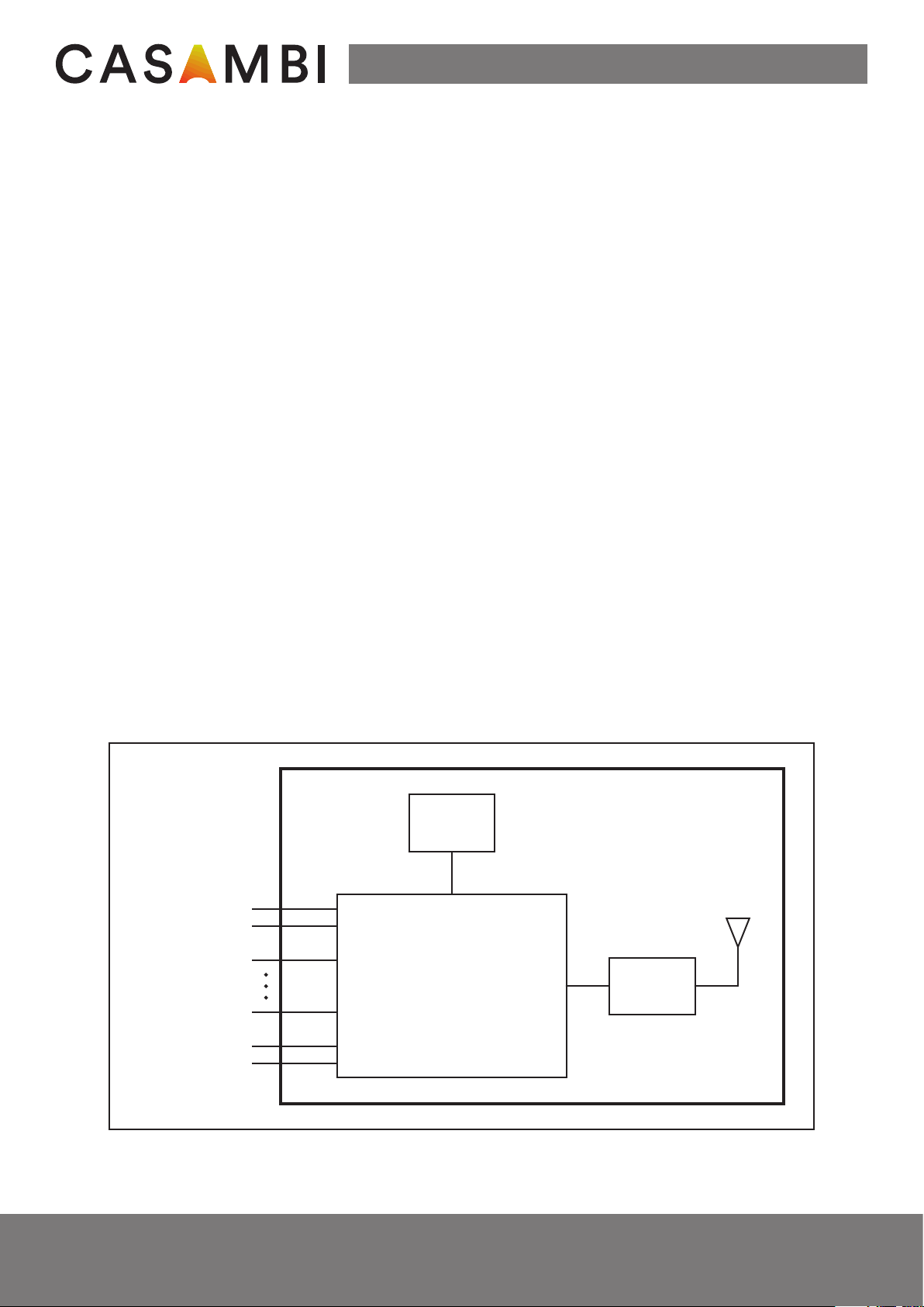
Casambi CBM-002A/B is an embedded wireless module with a powerful 32-bit ARM® Cortex™-M4 CPU and a
2.4 GHz transceiver with on-board antenna and optional matching circuitry. It can be integrated, for example,
into an LED driver, a light xture or an LED bulb.
CBM-002A/B has total of 12 GPIO pins, which can be congured to perform various tasks, such as SPI, TWI (I2C
compatible), UART, 4 channel PWM output and 3 channel Analog-to-Digital Converter input. Only the ADC
input channels have xed GPIO pins. Other functions can be freely congured to any GPIO pin.
CBM-002A/B is controlled wirelessly by a smart device with Casambi application. Multiple Casambi units form
automatically a mesh network, which can be controlled from any point. The network communicates directly
with the smart device using Bluetooth 4.0. No external gateway device or Wireless LAN network is needed.
CBM-002A/B has an integrated 2,4 GHz antenna. This will have to be taken into account when the device is
integrated to any environment. See chapter “14.5 Mounting” for further instructions.
The module can be operated also from a traditional on/off wall switch. By icking the switch on and off the
user can select different pre-set modes. These modes can affect one or several devices on the network. This
way the user does not have to have the smart device at hand all the time in order to select the desired settings
or modes. This feature requires an external electrolytic capacitor to supply power during power-off stage as
well as a power-on detection circuitry.
A large number of different setting of CBM-002A/B can be congured in Casambi Admin webpages and taken
into use without a need to re-program the module. These settings include, for example, I/O pin mapping,
PWM, push buttons, etc.
5 Block Diagram
Crystal,
32 MHz
VCC
GND
GPIO0
GPIO11
SWDCLK
SWDIO/nRESET
32 bit Cortex M4
RF-MCU
Matching
network
Picture 1. CBM-002A/B block diagram
Casambi Technologies Oy
Linnoitustie 4 A
02600 Espoo, Finland
Page 5 of 25
www.casambi.com
info@casambi.com
tel. +358 10 501 2950

CBM-002A/B
6 System Blocks
6.1 General Purpose I/O (GPIO)
CBM-002A/B has 12 General Purpose I/O pins. Each GPIO can be accessed individually and each has the following features:
• Input/output direction
• Congurable output drive strength
• Internal pull-up and pull-down resistors
• Buffered inputs
• Trigger interrupt on all pins (rising edge, falling edge, any change)
• Serial interface and PWM output can be freely congured to each pin
GPIO pins 0-3 also supports analog input signals when an internal Analog-to-Digital Converter (ADC) is used.
6.2 Analog-to-Digital Converter (ADC)
The up to 12-bit Analog-to-Digital Converter enables sampling of up to 4 external signals (GPIOs 0-3) through
a front-end multiplexer. The ADC has congurable input and reference prescaling, and sample resolution (8,
10, and 12-bit).
There are two options for the voltage reference:
• Internal 1,20 V reference
• VCC with 1/3 prescaling
Analog inputs can have a congurable gain of 1/6, 1/5, 1/4, 1/3, 1/2, 1, 2 and 4. The suitable voltage range
for ADC input is 0 V - VCC.
6.3 PWM Output
Any GPIO pin can be congured to output PWM signal. Up to 4 PWM channels can be used simultaneously.
PWM frequency can be determined freely up to 40 kHz. PWM frequency is the same with all PWM channels.
The maximum resolution is 400-1600 steps and it depends on the PWM frequency.
The PWM signal is logic level (max. VCC) and it has driving capacity from 4 mA (standard) up to 14 mA (highdrive). An adjustable analog voltage (0 V - VCC) can be derived from the PWM signal by an external RC lter.
A 10 kHz PWM signal together with a 10kΩ + 2,2 µF RC filter can be used as a starting point. Depending on
the application, it may be necessary to use an operational amplifier as a buffer stage.
+3 VDC
CBM-002A/B
10 kHz PWM 0-3V analog
GPIOx
Picture 2. Adjustable 0-10V output from PWM signal.
Page 6 of 25
Casambi Technologies Oy
Linnoitustie 4 A
02600 Espoo, Finland
G3,33 0-10V
output
www.casambi.com
info@casambi.com
tel. +358 10 501 2950

CBM-002A/B
7 Serial Interfaces
CBM-002A/B can be connected to an external MCU through its extension interface, which supports SPI, TWI
and UART. Through this interface it is possible to, for example, gather information from sensors through
Casambi network.
7.1 Serial Peripheral Interface (SPI)
CBM-002A/B supports a 3-wire (SCK, MISO, MOSI) bidirectional SPI bus with fast data transfers to and from
multiple slaves. CBM-002A/B acts as a master and it provides a simple CPU interface which includes a TXD
register for sending data and an RXD register for receiving data. These registers are double-buffered to enable some degree of uninterrupted data ow in and out of the SPI master.
Each of the slave devices requires an individual chip select signal which can be connected to any available
GPIO pin. The SPI master does not implement support for chip select directly. Therefore, the correct slave
must be selected independently of the SPI master.
The GPIOs used for each SPI interface line can be chosen from any GPIO on the module and are independently congurable. This enables great exibility in module pinout and enables efcient use of printed circuit
board space and signal routing.
The SPI peripheral supports SPI modes 0, 1, 2, and 3.
7.2 Two-Wire Interface (TWI)
The Two-Wire Interface (I2C compatible) can interface a bidirectional wired-AND bus with two lines (SCL,
SDA). The interface is capable of clock stretching and data rates of 100 kbps and 400 kbps are supported. The
TWI transmitter and receiver are single buffered.
The GPIOs used for each Two-Wire Interface line can be chosen from any GPIO on the module and are independently congurable. This enables great exibility in module pin-out and enables efcient use of board
space and signal routing.
7.3 Universal Asynchronous Receiver/Transmitter (UART)
The Universal Asynchronous Receiver/Transmitter offers fast, full-duplex, asynchronous serial communication
with built-in ow control support in HW up to 1 Mbps baud. Parity checking and generation for the 9th data
bit are supported.
The GPIOs used for each UART interface line can be chosen from any GPIO on the module and are independently congurable. This enables great exibility in module pinout and enables efcient use of board space
and signal routing.
Casambi Technologies Oy
Linnoitustie 4 A
02600 Espoo, Finland
Page 7 of 25
www.casambi.com
info@casambi.com
tel. +358 10 501 2950
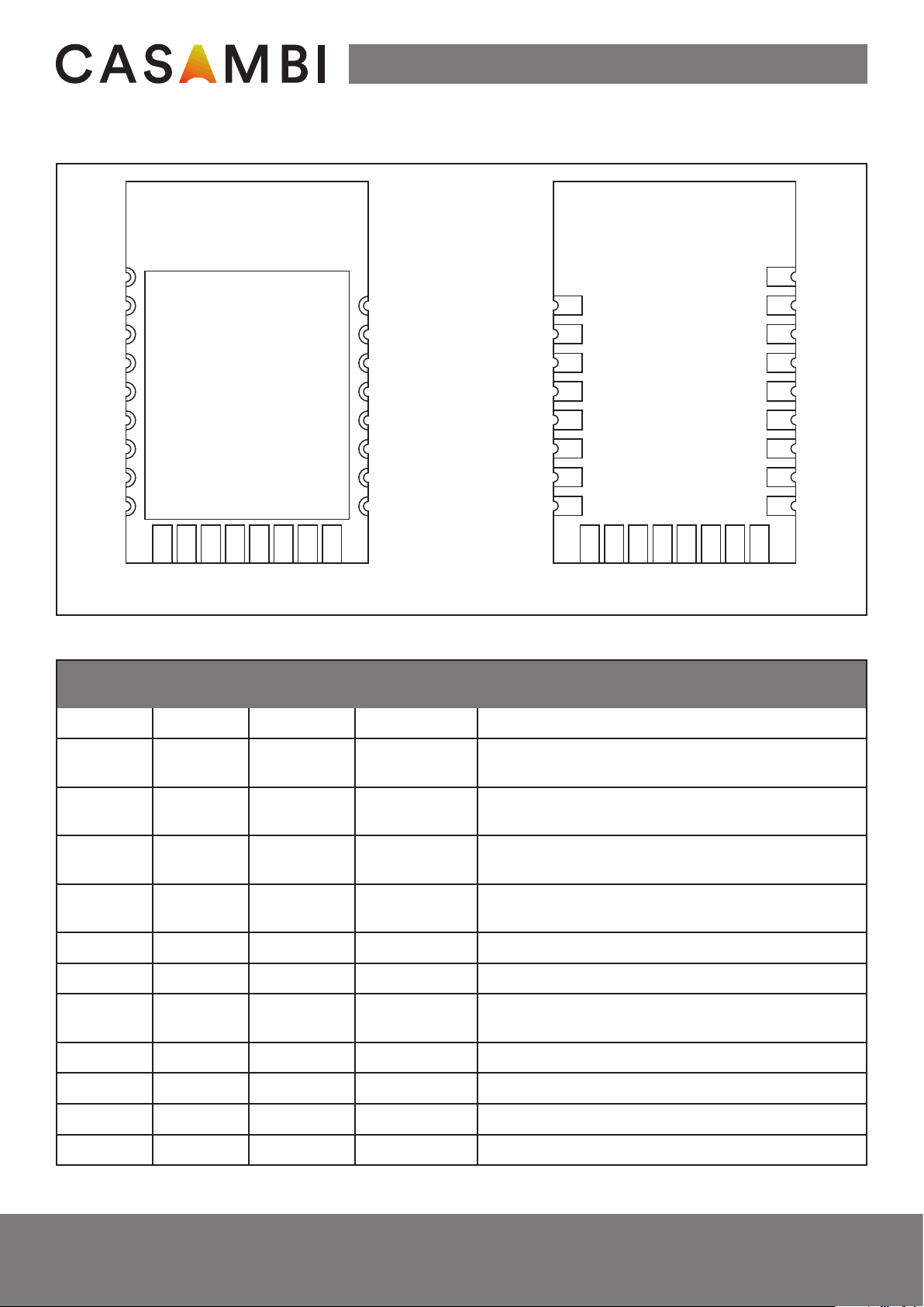
8 Pin Assignment
CBM-002A/B
H0
H1
H2
H3
H4
CBM-002A/B
H16
H15
H14
H13
Top View
H5
H6
H7
H8
V0V1V2V3V4V5V6
Picture 2. Pin assignment
Horizontal
Pin
H0 - GND Power Ground
Vertical
Pin
Pin Name Pin Function Description
H12
H11
H10
H9
V7
H16
H15
H14
H13
H12
H11
H10
H9
CBM-002A/B
Bottom View
V8
V9
V10
V11
V12
V13
V14
H0
H1
H2
H3
H4
H5
H6
H7
H8
V15
H1 V7
H2 V6
H3 V5
H4 V4
H5 V3 VCC Power Power supply
H6 V2 SWDCLK Digital input HW debug and ash programming I/O
H7 V1
H8 V0 GND Power Ground
H9 V8 GPIO4 Digital I/O General purpose I/O pin
H10 V9 GPIO5 Digital I/O General purpose I/O pin
H11 V10 GPIO6 Digital I/O General purpose I/O pin
GPIO0
AIN0
GPIO1
AIN1
GPIO2
AIN2
GPIO3
AIN3
SWDIO
nRESET
Digital I/O
Analog input
Digital I/O
Analog input
Digital I/O
Analog input
Digital I/O
Analog input
Digital I/O
Analog input
Page 8 of 25
General purpose I/O pin
ADC input 0
General purpose I/O pin
ADC input 1
General purpose I/O pin
ADC input 2
General purpose I/O pin
ADC input 3
HW debug and ash programming I/O
System reset (active low)
Casambi Technologies Oy
Linnoitustie 4 A
02600 Espoo, Finland
www.casambi.com
info@casambi.com
tel. +358 10 501 2950
 Loading...