

Page 1
User’s Manual
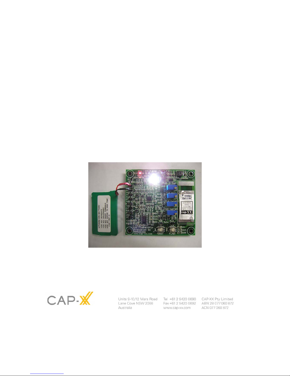
Camera Phone Flash
Evaluation Board
APPEB1006
All information contained herein is strictly confidential APPEB1006 User Manual rev1.0, 31-May-2005 page 1 of 6
© CAP-XX Pty Limited 2005
Page 2

All information contained herein is strictly confidential APPEB1006 User Manual rev1.0, 31-May-2005 page 2 of 6
© CAP-XX Pty Limited 2005
Camera Phone Flash Evaluation Board User’s Manual
Board Features
FLASH mode with adjustable voltage and current
TORCH/MOVIE mode with adjustable voltage and current
Vin and Vout indicating LED’s
On-board or External triggering
On-board or External white LED
LED and inductor current measurement ability
Undervoltage lockout (UVLO)
Boost enable/disable during flash and torch for different power architectures
Auto run for flash or torch
Quick Setup
The following jumpers should be in place J2, J5, J7, J8 and J10. Connect the positive
terminal of a single cell Lithium Ion rechargeable battery (3.3V-4.2V) to any pin on J1 and
connect the negative terminal to any pin of J3. The red LED (D1) should come on
immediately and the yellow LED (D2) should increase in brightness over a few seconds
whilst the supercapacitor charges up.
When the TORCH push button (SW1) is pressed 100mA will flow through the white LED
(D5). At 100mA the button can be held down continuously.
When the FLASH push button (SW2) is pressed 1A will flow through the white LED (D5) for
approximately 80ms. If the button is held down continuously the flash will retrigger
approximately every 2.5s. This duty cycle is imposed due to the thermal constraints of the
white LED.
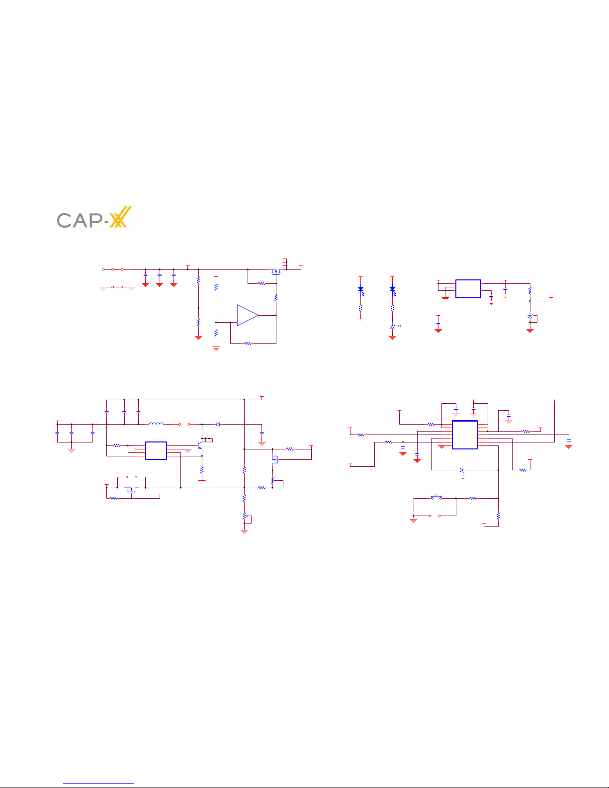
Circuit Description (refer to schematics at the end of this manual)
Input Voltage
The circuit is designed to operate from an external Li ion battery (4.2V-3.3V).
Vbat is the node connected to the battery via J1.
J1 is to be connected to battery positive terminal. Pins 1 and 2 of J1 are joined.
J3 is to be connected to battery negative terminal. Pins 1 and 2 of J3 are joined.
An undervoltage lockout (UVLO) has been included (U2B) such that when the battery voltage
drops below 3.1V the main switch (MOSFET M1) opens. It will reclose with 350mV of
hysteresis (3.45V). The 3V regulator remains operational during a UVLO.
The main reason for the UVLO is that the boost controls Vout which is the sum of the input
voltage (battery or perhaps bench top supply) plus the supercap (C1) voltage. The voltage
across the supercap is not measured. Therefore, if the input voltage was say 3V and Vout
was controlled to be 5.7V then the supercap would be at 2.7V which reduces its life. For
maximum life the supercap should be kept below 2.3V. However, the supercapacitor voltage
can be increased to 2.5V for short periods, such as while taking flash photos, without
affecting life.
Indicating LED’s
D1 is a red LED that indicates a source voltage is present and that a UVLO has not occurred.
D2 is a yellow LED and indicates that Vout is present and above approximately 5V.
Page 3

All information contained herein is strictly confidential APPEB1006 User Manual rev1.0, 31-May-2005 page 3 of 6
© CAP-XX Pty Limited 2005
Boost Converter
J2 needs to be jumpered for normal operation. This jumper has been included so a wire loop
can easily be inserted to measure the inductor current. By measuring the inductor current
and monitoring the base drive voltage of Q1 the current through Q1, D3 and supercap can
also be determined.
J4 is not jumpered during normal operation. This jumper has been included to manually
disable the boost if required. If jumpered it forces the feedback voltage at pin 6 of the boost
to be 3V which is >> than the 730mV of the internal reference thereby instructing the boost to
cease switching.
The boost can also be disabled by pulling the gate of M3 low. This can be done automatically
during a FLASH pulse by jumpering J7 or while in TORCH mode by jumpering J10.
The advantage of disabling the boost during a FLASH pulse is that the maximum battery
current is equal to the load (flash LED) current, however, the disadvantage is that the
supercap discharge current is also equal to the load current and it will discharge at a faster
rate than if the boost was enabled. The disadvantage of enabling the boost during a Flash
pulse is that the maximum battery current is greater or much greater then the load current
depending on the current limit set on the boost.
FLASH MODE
The boost generates an output voltage (Vout) that is > the battery voltage. For FLASH mode,
Vout is factory set to 5.7V. This voltage can be increased by turning R17 (a 2k pot)
anticlockwise. Care must be taken if this voltage is increased not to overvoltage the
supercap, ie the supercap voltage will be Vout minus the voltage of the battery. For
maximum supercapacitor life the voltage should be kept below 2.3V however short term
overvoltages (seconds) may go up to 2.7V.
TORCH MODE
The continuous current required for TORCH is << FLASH current (typically 100mA Vs 1A).
Therefore the voltage dropped across the LED will be less. To increase efficiency (and to
reduce thermal stress on the current limiting MOSFET (M4)) Vout should also be reduced.
There are two options for the TORCH Vout, if constant high output light is more important
than efficiency then option a) should be chosen.
a) In this option the Boost is enabled with J10 removed and J11 is jumpered. Vout can
be adjusted using R12 (a 500k pot). Vout is factory set to 4.2V. This means that Vout
will always be > Vin irrespective of the battery voltage. In this mode the forward
voltage to drive the LED at 200mA, for example, will always be available even when
the battery nears its end voltage (3.3V).
b) In this option the Boost is disabled with J10 jumpered and J11 is don’t care. This
means Vout will always be equal to Vin minus the drops incurred by the inductor’s
(L1) DC resistance and D3. This is the most efficient mode because the current
limiting MOSFET (M4) does not have to drop as many volts and the Boost is not
operating. However, depending on the LED current required, there may not be
enough voltage headroom in Vout when the battery nears its end voltage (3.3V). For
example, if the LED current was chosen to be 200mA and the voltage across a typical
LED at this current was also 3.3V then there would be no volts available across the
current sense resistor (R22) and M4 and then only say 150mA would be available.
Option b) is factory chosen and the TORCH current is set to 100mA.
Page 4

All information contained herein is strictly confidential APPEB1006 User Manual rev1.0, 31-May-2005 page 4 of 6
© CAP-XX Pty Limited 2005
The user must decide on what is the end voltage of the Li ion battery and what
current gives acceptable light for the Torch. Of course the user may also decide that it
is acceptable to have slightly less light output as the battery nears its end voltage
(after all, most users are familiar with this behavior in an incandescent torch).
Current Control
The FLASH current is factory set to 1.0 Amp. It can be reduced by turning R25 (10k pot) anticlockwise. The maximum LED current rating is 2 Amps. The FLASH current needs to be
adjusted prior to the TORCH current because the FLASH setting affects the TORCH setting
but not vice versa.
The TORCH current is factory set at 100mA. It can be reduced by turning R26 (2k pot) anticlockwise.
External Flash LED
An External white LED (or other load) can be connected to the board via J5. This also
requires that the on-board LED (D5) be bypassed with J6. Alternatively, a second flash LED
(LXCL-PWF1) can be connected in parallel to D5 across J6 (pin 2 is +ve).
AutoTorch/External Torch Mode Control
If J12 is jumpered, then Torch mode will be permanently on (Auto Torch). Alternatively, an
external control signal connected to pin 2 of J12 will select Torch mode when Hi (3V – 5V).
This logic signal drives the gates of M8, M9, and M10 and must source 0.1mA to develop
3.3V across R36.
Flash PulseTimers/External Flash Pulse Control
There are two on-board 555 timers. One generates the FLASH on-time and the other
generates the off-time. The FLASH trigger from these timers is connected to the Current
Control circuitry via J8. J8 is jumpered for normal operation. An external triggering circuit can
be connected by removing the jumper from J8 and connecting the external signal to pin 1 of
J8. There is a 33k pull down resistor on this pin. A logic high signal on this pin will take a
FLASH. Make sure that this signal is < 100ms long and does not occur for at least another 2s
otherwise the thermal limits of the white LED (D5) will be violated and it will be destroyed.
Auto Flash
If J13 is jumpered then the two 555 timers will be continuously triggered to generate an 80ms
flash pulse every 2.5s.
Further Information
CAP-XX will be pleased to provide further information on the applications described here,
and on the use of supercapacitors in any application. Please use the contact details on the
header page, or visit the cap-XX web site.
Page 5
Schematics
6
LEDpulse
R32
150k
805
Vbat
R3
47k
805
R18
33k
805
Vout
3V
C19
100n
805
M3
FDV302P
SOT23
D1
LSR976
805
SW2
Flash
B3SN
R12
T93YB
500k
3
1
2
Q1
ZXT13N50DE6
SOT23-6
3
1425
6
3V
C21
100n
805
J13
Auto Flash
1 2
3V
R13
1e6
805
C16
10u
805
C4
10u
805
J4
Manual Boost Disable
1 2
D6
BAT754
SOT23
1 3
2
C2
10u
805
D3
MBRA130LT3
SMA
D4
BZX84C-4V7
SOT23
1 3
2
3V
R29
680k
805
Vin
R2
33k
805
1V2
Vbat
C6
10u
805
R4
1k
805
M1
FDC638P
SuperSOT-6
3
421
5
R34
3k3
805
Vout
C8
DNP 10u
805
R5
1k
805
C10
DNP 10u
805
C12
100n
805
U3
TC1185
SOT23-A
1
2
3 4
5
Vin
GND
*Shdn Bypass
Vout
U1
ZXSC100
SO8
1
2
3
4 5
6
7
8
EM
BAS
RE
VCC Isense
FB
GND
Vdrive
Vin
C3
10u
805
R14
1k
805
*Boost Disable
3V
1V2
3V
R11
47k
805
C11
10u
805
C18
100n
805
D2
LYR976
805
J2
Inductor Current
1 2
R37
150
805
R10
100k
805
R1
82k
805
R8
18k
805
R17
T93YB
2k
3
1
2
R28
220k
805
C7
10u
805
R30
33k
805
3V
U5
TLC556CD
SOIC
1
2
3
4
5
6
7 8
9
10
11
12
13
14
DIS
TH
CON
RES
OUT
TRIG
GND TRIG
OUT
RES
CON
TH
DIS
VCC
Vbat
Offtime Trigger
Undervoltage Lockout
Vmin = 3.1V with
350mV Hysteresis
C20
47n
805
U2B
TS1852
7
5
6
OUT
+
-
R15
33k
805
R6
3R3
805
C1
GW101
R9
R047
805
M2
FDV302P
SOT23
C9
DNP 10u
805
C13
10u
805
Torch Vout
J1
Vbattery
1 2
3V
L1
33u
ELL6RH
1 2
C5
10u
805
R7
33k
805
J3
GND
1 2
R35
33k
805
R33
33k
805
U4
LM4041
2 1
3
R16
14k3
805
Vin
C17
100n
805
All information contained herein is strictly confidential APPEB1006 User Manual rev1.0, 31-May-2005 page 5 of 6
© CAP-XX Pty Limited 2005
Page 6

All information contained herein is strictly confidential APPEB1006 User Manual rev1.0, 31-May-2005 page 6 of 6
© CAP-XX Pty Limited 2005
R27
1M5
805
R25
T93YB
10k
3
1
2
1V2
Torch Vout
Vout
J11
Torch Voltage
1
2
J6
LED Bypass
1
2
R21
150
805
U2A
TS1852
SO
1
3
2
8
4
OUT
+
-
VccVdd
M7
FDV301N
M5
FDV301N
J8
External Timer
1
2
R24
33k
805
Offtime Trigger
R26
T93YB
2k
3
1
2
3V
C15
220p
603
R20
33k
805
J7
Pulse Boost Disable
1
2
*Boost Disable
R19
100k
805
1V2
R36
33k
805
J10
Torch Boost Disable
1
2
SW1
TorchB3SN
M4
ZXM64NO2X
MSOP8
1
4
5
7
8
6
2
3
R22
R047
805
3V
3V
M8
FDV301N
R31
33k
805
*Boost Disable
M6
FDV301N
Pulse
R23
3k3
805
3V
Torch/*Flash
J9
GND
1
2
D5
LumiLED
?
M10
FDV301N
J12
Auto Torch
1
2
LEDpulse
M9
FDV301N
C14
100n
805
J5
LED Current
1
2
 Loading...