Cambridge Audio DVD-89 Service manual
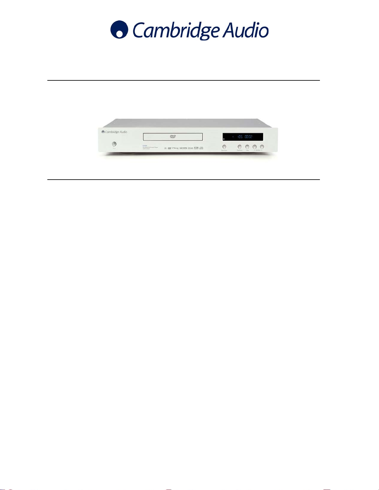
DVD89
Issue Date: 27th February 2006
SERVICE MANUAL
SPECIFICATIONS:
Disc Types DVD, DVD-A, DVD-V, CD-RW
CD-R, CD-DA, DIVX, SACD
Audio Formats 5.1 and Stereo Downmix
LPCM 16 bit 44.1kHz
Dolby Digital 5.1 24 bit 96kHz
DTS Output (Digital Audio Out Only)
DVD Audio 2 Channel 24 bit 192kHz
DVD Audio 5.1 (MLP) 24 bit 96kHz
Video Composite Video (CVBS)
S-Video (SVHS)
RGB
DVI-D & HDMI
Component (YCbCr)
PAL/NTSC
Interlaced / Progressive Scan
THD (unweighed) < 0.01%
Dynamic Range >100dB
Frequency Response 20Hz – 20kHz
Video Amplitude 1.0V pk-pk (75 ohms)
S-Video Amplitude Y:1.0V pk-pk n (75ohms)
C: 0.286V pk-pk (75 ohms)
Power Supply 100-240V AC~50/60Hz
Max Power Consumption 40W
Dimensions mm (H x W x D) 55 x 430 x 263
Weight (kg) 2.56 kg AP19841/1
Gallery Court Hankey Place London SE1 4BB UK
Tel: +44 (0)20 7940 2200 Fax: +44 (0)20 7940 2233

DVD89 SERVICE MANUAL
TABLE OF CONTENTS
Safety Precautions
Front Panel Illustration
Prevention of Static Electricity Discharge
Mechanism Unit Exploded Diagram
Bracket Exploded View and Parts List
Protection of the Laser Diode
Video Output Confirmations – Luminance & Chrominance Signal
HY57V641620HG Pin Configuration & Description (U211)
HY57V641620HG Functional Block Diagram (U211)
MT1392 Pin Definitions (U203)
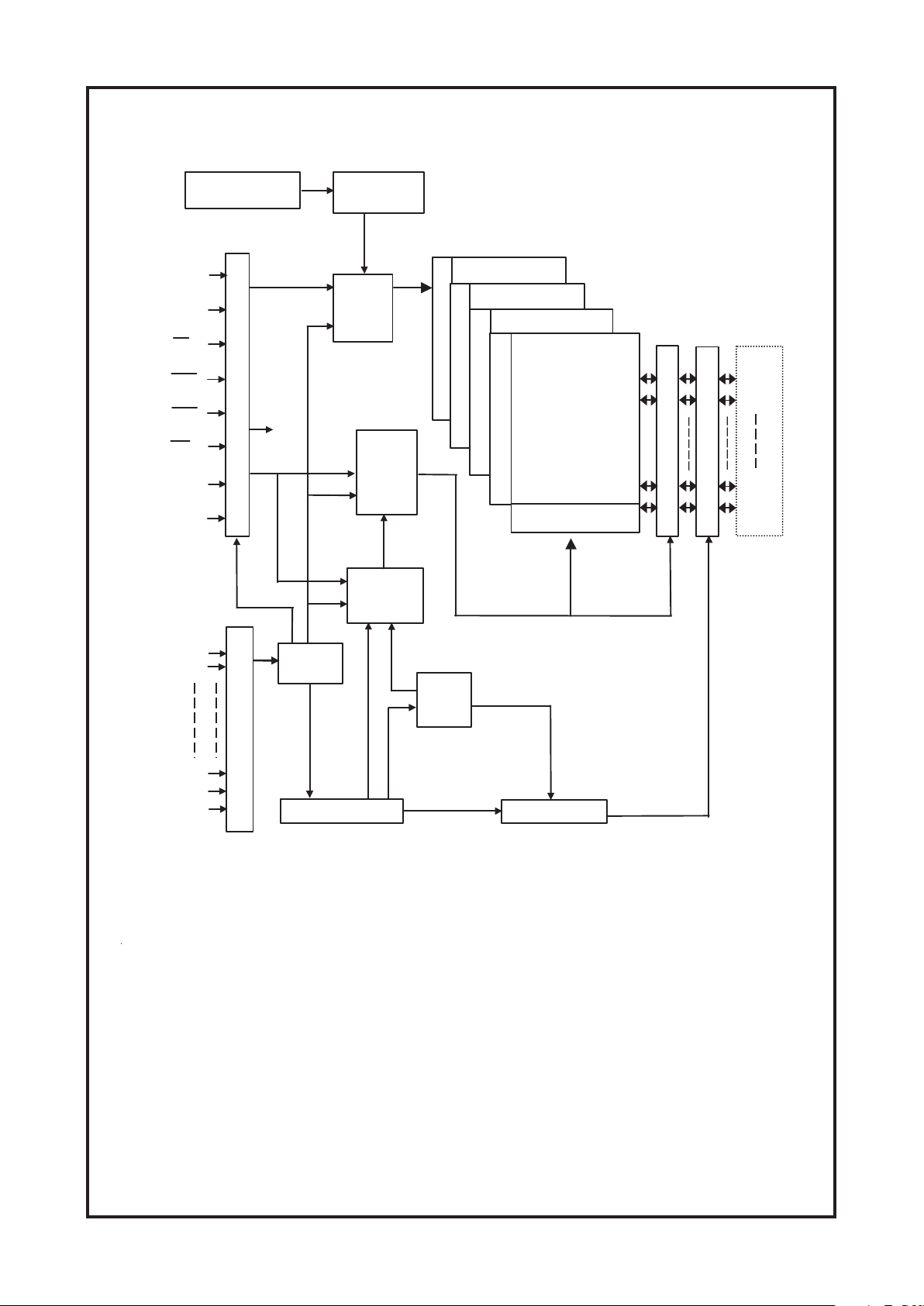
MT1392 System Configuration & Functional Block (U201)
MT1392 Functions (U201)
MT1392 Pinout Diagram (U201)
MT1389 Pinout Diagram (U201)
MT1389 Block Diagram (U201)
MT1389 Pin Function (RF Interface) (U201)
MT1389 Pin Function (Analog Monitor Output) (U201)
MT1389 Pin Function (General Power / Ground, Micro Controller & Flash Interface) (U201)
MT1389 Pin Function (Micro Controller & Flash Interface) (U201)
MT1389 Pin Function (Audio Interface) (U201)
MT1389 Pin Function (Video Interface) (U201)
MT1389 Pin Function (DRAM Interface) (U201)
MT1389 Pin Function (DRAM Interface & JTAG Interface) (U201)
Front Panel & VFD Schematic
Front Panel & VFD Board Layout
Power Supply Schematic
Power Supply PCB Layout
Main PCB Board (Main Processor)
Main PCB Board (Memory, Reset & Main Clock)
Main PCB Board (Audio DACS, Output Filters & Mute)
Main PCB Board (DVI & HDMI)
Main PCB Board (Video Outputs)
Main PCB Board Layout
Power Board Parts List
Main Panel Parts List
Decode Board Parts List
Serviceable Parts List
3
4
5
6
7
8
9
10
11
12/13/14
15
16
17
18
19
20
21
22
23
24
25
26/27
28
29
30
31
32
33
34
35
36
37
38
39
40
41/42
43

Cambridge Audio DVD89 DVD Player
1. When servicing, observe the original lead dress. if a short circuit is found, replace all parts which have
been overheated or damaged by the short circuit.
2. After servicing, see to it that all the protective devices such as insulation barrier, insulation papers
shields are properly installed.
3. After servicing, make the following leakage current checks to prevent the customer from being exposed
to shock hazards.
Some semiconductor(solid state)devices can be damaged easily by static electricity. Such components
commonly are called Electrostatically Sensitive(ES)Devices. Examples of typical ES devices are integrated
circuits and some field-effect transistors and semiconductor chip components. The following techniques
should be used to help reduce the incidence of component damage caused by electro static discharge(ESD).
1. Immediately before handling any semiconductor component or semiconductor-equipped assembly, drain
off any ESD on your body by touching a known earth ground. Alternatively, obtain and wear a commercially
available discharging ESD wrist strap, which should be removed for potential shock reasons prior to
applying power to the unit under test.
2. After removing an electrical assembly equipped with ES devices,place the assembly on a conductive
surface such as alminum foil, to prevent electrostatic charge buildup or exposure of the assembly.
3. Use only a grounded-tip soldering iron to solder or unsolder ES devices.
4. Use only an anti-static solder removal device. Some solder removal devices not classified as anti-static
(ESD protected)can generate electrical charge sufficient to damage ES devices.
5. Do not use freon-propelled chemicals. These can generate electrical charges sufficient to damage ES
devices.
6. Do not remove a replacement ES device from its protective package until immediately before you are
ready to install it. (Most replacement ES devices are packaged with leads electrically shorted together by
conductive foam, alminum foil or comparable conductive material).
7. Immediately before removing the protective material from the leads of a replacement ES device, touch
the protective material to the chassis or circuit assembly into which the device will be installed.
Caution
Be sure no power is applied to the chassis or circuit, and observe all other safety precautions.
8. Minimize bodily motions when handling unpackaged replacement ES devices. (Otherwise harmless motion
such as the brushing together of your clothes fabric or the lifting of your foot from a carpeted floor can
generate static electricity(ESD).
COPYRIGHT NOTICE.
© 2005 Audio Partnership PLC. All rights reserved.
Cambridge Audio is a registered trademarks of Audio Partnership PLC. This document may not
be reproduced, distributed, transmitted, displayed, published, or broadcast without the express
written prior permission of Audio Partnership PLC.
Alteration or removal of any trademark, copyright, or other notice from this content is prohibited.
Information provided in this document is provided solely for the use of official service agents in
repairing and servicing Audio Partnership PLC products.
Safety Precautions

Cambridge Audio DVD89 DVD Player
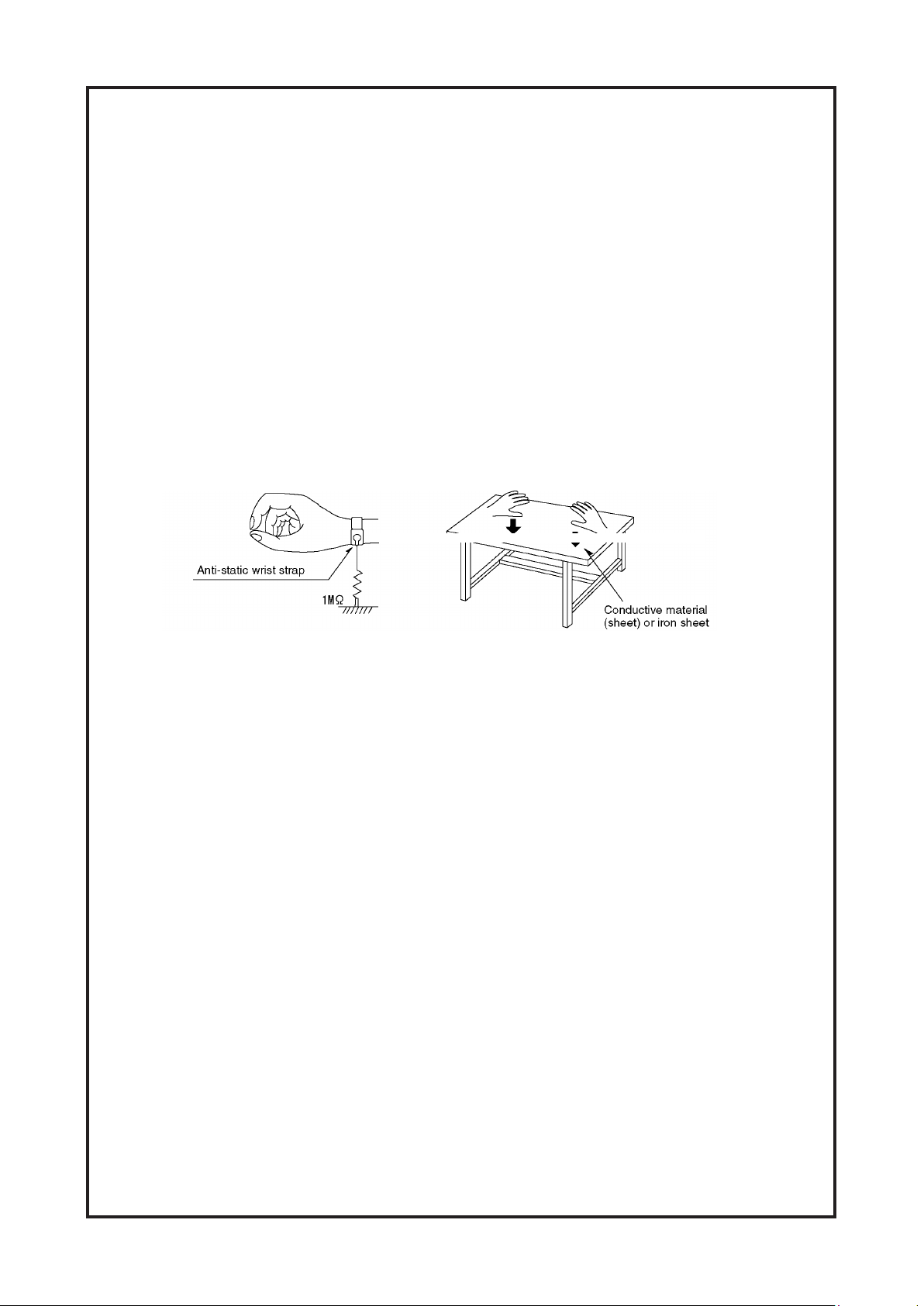
POWER switch
2
Disc tray
3
Display window
4
OPEN/CLOSE button
5
PLAY/PAUSE button
6
STOP button
2
4
7
Skip/Scan button
3
7
6
5
Front Panel Illustration
Cambridge Audio DVD89 DVD Player
The laser diode in the traverse unit (optical pickup)may brake down due to static electricity of clothes or human
The laser diode in the traverse unit (optical pickup) may break down due to static electricity of clothes or human
body. Use due caution to electrostatic breakdown when servicing and handling the laser diode.
Some devices such as the DVD player use the optical pickup(laser diode)and the optical pickup will be damaged
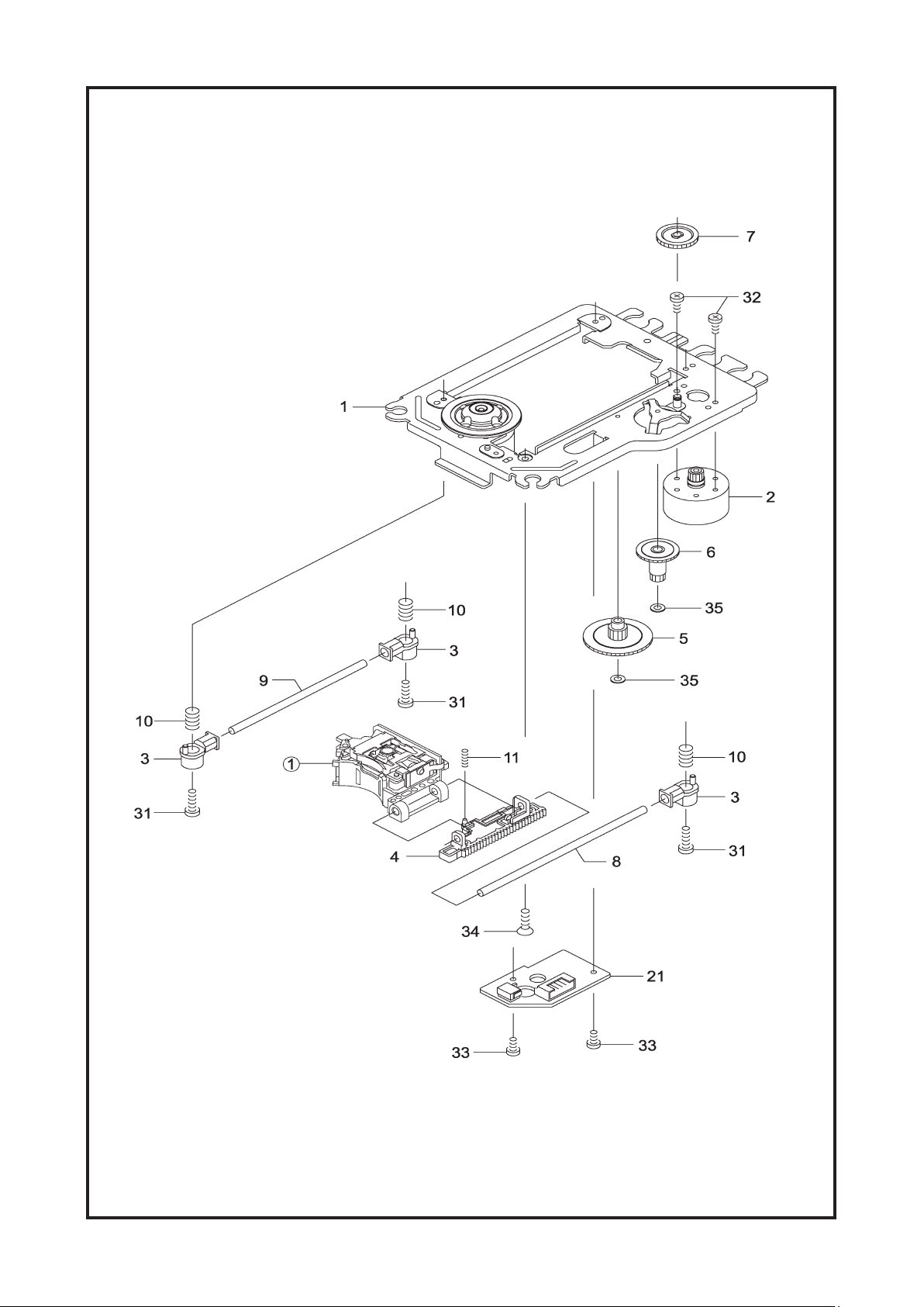
1. Grounding for electrostatic breakdown prevention
Some devices such as the DVD player use the optical pickup (laser diode) and the optical pickup will be
damaged by ststic electricity in the working enviroment. Proceed servicing works under the working
enviroment where grounding works is completed.
2. Worktable grounding
Put a conductive material sheet on the area where the optical pickup is placed, and ground the
sheet.
3. Human body grounding
Use the anti-static wrist strap to discharge the static electricity from your body.
sa fety_3 (157 7x40 9x2 tiff)
4. Handling of optical pickup
5. To keep the good quality of the optical pickup maintenance parts during transportation and before
installation, the both ends of the laser diode are short-circuited.After replacing the parts with new ones,
remove the short circuit according to the correct procedure. (See this Technical Guide).
6. Do not use a tester to check the laser diode for the optical pickup .This will damage the laser
diode due to the power supply in the tester.
7. Handling precautions for Traverse Unit (Optical Pickup)
8. Do not give a considerable shock to the traverse unit(optical pickup)as it has an extremely high-precise
structure.
9. When replacing the optical pickup, install the flexible cable and cut is short land with a nipper. See the
optical pickup replacement procedure in this Technical Guide. Before replacing the traverse unit, remove
the short pin for preventingstatic electricity and install a new unit. Connect the connector as quickley as
possible.
10. The flexible cable may be cut off if an excessive force is applied to it. Use caution when handling the cable.
11. The half-fixed resistor for laser power adjustment cannot be adjusted. Do not turn the resistor.
Prevention of Static Electricity Discharge
Cambridge Audio DVD89 DVD Player
Mechanism Unit Exploded Diagram
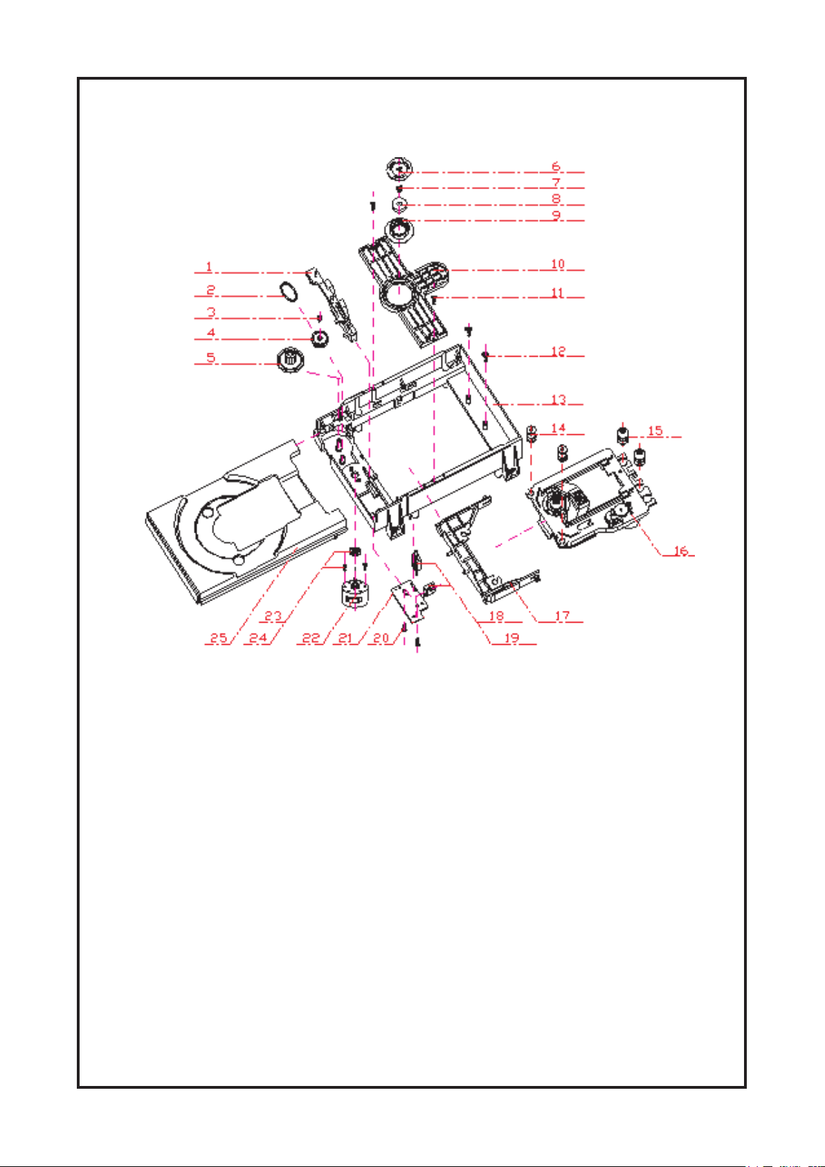
Cambridge Audio DVD89 DVD Player
1) Bracket
2) Belt
3) Screw
4) Belt Wheel
5) Gear Wheel
6) Iron Chip
7) Immobility Mechanism Equipment
8) Magnet
9) Platen
10) Bridge Bracket
11) Screw
12) Screw
13) Big Bracket
14) Front Silicon Rubber
15) Back Silicon Rubber
16) Pick Up
17) Pick Up
18) Switch
19) Five Pin Flat Plug
20) Screw
21) PCB
22) Motor
23) Moto Wheel
24) Screw
25) Tray
Bracket Exploded View and Parts List

Cambridge Audio DVD89 DVD Player
Laser Diode Protection Shorts (Replacement Parts)
Cautions on assembly and adjustment
Make sure that the workbenches, jigs, tips, tips of soldering irons and measuring instruments are grounded,
and that personnel wear wrist straps for ground.
For replacement optical pickups open the LD short lands quickly with a soldering iron after
circuit is connected.
Refrain from operation and storage in atmospheres containing corrosive gases (such as H2S,SO2,
NO2 and Cl2)or toxic gases or in locations containing substances(especially from the organic silicon,cyan,
formalin and phenol groups)which emit toxic gases.It is particularly important to ensure that none of the
above substances are present inside the unit.Otherwise,the motor may no longer run.
Protection of the Laser Diode

Cambridge Audio DVD89 DVD Player
Screwdriver,Oscilloscope
Do these confirmations after replacing a P.C.B. - (Luminance Signal)
Measurement point
Video output terminal
Measuring equipment,tools
200mV/dir,10 sec/dir
Purpose:To maintain video signal output compatibility.
1.Connect the oscilloscope to the video output terminal and terminate at 75 ohm.
2.Confirm that luminance signal(Y+S)level is 1000mVp-p±30mV
PLAY(Title 46):DVDT-S15
PLAY(Title 12):DVDT-S01
Mode Disc
Color bar 75%
Confirmation value
1000mVp-p±30mV
(Chrominance Signal)
Measurement point
Video output terminal
Measuring equipment,tools Confirmation value
200mV/dir,10 sec/dir
Purpose:To maintain video signal output compatibility.
1.Connect the oscilloscope to the video output terminal and terminate at 75 ohm.
2.Confirm that the chrominance signal(C)level is 621 mVp-p±30mV
PLAY(Title 46):DVDT-S15
PLAY(Title 12):DVDT-S01
Mode Disc
Color bar 75%
621mVp-p±30mV
Video Output Confirmations - Luminance & Chrominance Signal

PIN CONFIGURATION
Cambridge Audio DVD89 DVD Player
VDD
DQ0
VDDQ
DQ1
DQ2
VSSQ
DQ3
DQ4
VDDQ
DQ5
DQ6
VSSQ
DQ7
DD
V
LDQM
/WE
/CAS
/RAS
/CS
BA0
BA1
A10/AP
A0
A1
A2
A3
DD
V
1
2
3
4
5
6
7
8
9
10
11
12
13
14
15
16
17
18
19
20
21
22
23
24
25
26
27
54pin TSOP II
400mil x 875mil
0.8mm pin pitch
VSS
54
DQ15
53
VSSQ
52
DQ14
51
DQ13
50
VDDQ
49
48
DQ12
47
DQ11
VSSQ
46
DQ10
45
44
DQ9
43
VDDQ
42
DQ8
SS
V
41
NC
40
UDQM
39
CLK
38
CKE
37
NC
36
35
A11
A9
34
A8
33
A7
32
31
A6
A5
30
A4
29
SS
V
28
PIN DESCRIPTION
PIN PIN NAME DESCRIPTION
CLK Clock
CKE Clock Enable
CS Chip Select Enables or disables all inputs except CLK, CKE and DQM
BA0,BA1 Bank Address
A0 ~ A11 Address
Row Address Strobe,
RAS, CAS, WE
LDQM, UDQM Data Input/Output Mask Controls output buffers in read mode and masks input data in write mode
DQ0 ~ DQ15 Data Input/Output Multiplexed data input / output pin
VDD/VSS Power Supply/Ground Power supply for internal circuits and input buffers
VDDQ/VSSQ Data Output Power/Ground Power supply for output buffers
NC No Connection No connection
Column Address Strobe,
Write Enable
The system clock input. All other inputs are registered to the SDRAM on the
rising edge of CLK
Controls internal clock signal and when deactivated, the SDRAM will be one
of the states among power down, suspend or self refresh
Selects bank to be activated during RAS activity
Selects bank to be read/written during CAS activity
Row Address : RA0 ~ RA11, Column Address : CA0 ~ CA7
Auto-precharge flag : A10
RAS, CAS and WE define the operation
Refer function truth table for details
(U211) HY57V641620HG Pin Configuration & Description
Cambridge Audio DVD89 DVD Player
I/O Buffer & Logic
1Mbit x 4banks x 16 I/O Synchronous DRAM
Self refresh logic
CLK
CKE
CS
RAS
CAS
WE
UDQM
LDQM
& timer
State Machine
Bank Select
Row active
refresh
Column
Active
Internal Row
counter
Row
Pre
Decoders
Column
Pre
Decoders
Column Add
Counter
1Mx16 Bank 3
X decoders
X decoders
1Mx16 Bank 2
1Mx16 Bank 1
X decoders
X decoders
1Mx16 Bank 0
Memory
Cell
Array
Y decoders
Sense AMP & I/O Gate
DQ0
DQ1
DQ14
DQ15
A11
BA0
BA1
A0
A1
Address
Address buffers
Registers
Mode Registers
Burst
Counter
CAS Latency
Data Out Control
Pipe Line Control
(U211) HY57V641620HG Functional Block Diagram

Cambridge Audio DVD89 DVD Player
Pin number Symbol Type Description
1 DVSS GND Digital ground
2-9 C0-C7 I, PD Normal : Digital chroma input
VDAC test : DAC test mode [0:7] input.
BIST mode : BIST data input
10 DVDD33 VDD Digital power, 3.3V
11 VCK I Clock of digital video input
12 DVSS GND Digital ground
13-20 Y0-Y7 I, PD Normal : Digital luma input
VDAC test : DAC test data [0:7] input.
BIST mode : BIST address input
21 SSCK I
22 SSD IO Slave serial interface data input/output
23 DVDD18 VDD Power of digital core, 1.8V
24 PWDN# I, PU Power down, actiev low
25 RST# I, PU Reset, active low
26 XTAL I Normal : clock input
27 INT O
28 DVSS GND Digital ground
29 A7/GPO0 IO,PD
30 A6/GPO1
31 TRAP2/GP02
TRAP1/GP03
TRAP0/GP04
Trap Mode
bit 2 1 0
0 0 0 Normal,
1 A1 A0 Normal, with master 12C enable
0 0 1 Test scan mode
0 1 0 VDAC test mode
0 1 1 BIST
34 MSCK/GPO5 O MasterI2C on : Master serial interface clock output
IO,PD
IO,PD
IO,PD
IO,PD
with master 12C disable
A(1:0) : EEPROM device address select
mode
Normal : Slave serial interface clock input
SCAN mode : scan reset, active low
VDAC test: VDAC test clock imput
Interrupt output
Power On: Serial interface address 7
BIST mode : SRAM fail output
Normal : General purpose output
Power On: Serial interface address 6
BIST mode : SRAM fail output
Normal : General purpose output
Power On: Hardware trap bit 2
BIST mode : SRAM fail output
Normal : General purpose output
Power On: Hardware trap bit 1
BIST mode : SRAM fail output
Normal : General purpose output
Power On: Hardware trap bit 0
BIST mode : SRAM fail output
Normal : General purpose output
BIST mode : SRAM fail output
Normal : General purpose output
(U203) MT1392 Pin Definitions

Cambridge Audio DVD89 DVD Player
Pin number Symbol Type Description
MSD/GPO6 IO,PU MasterI2C on : Master serial interface data input/output
BIST mode : SRAM fail output
Normal : General purpose output
36 GPO7 IO,PD PowerON : EPROM word-address type. 1 : 16bit , 0 : 8bit
BIST mode : SRAM fail output
Normal : General purpose output
37 GPIO8 IO BIST mode : SRAM fail output
Normal : General purpose output / HDMI test input / down-mixed audio input
38 GPIO9 IO BIST mode : SRAM fail output
Normal : General purpose output / V-sync inout / HDMI test input
VDAC test : PLL test enable
39 GPIO10 IO BIST mode : SRAM fail output
Normal : General purpose output / H-sync inout / HDMI test input
VDAC test : PLL test calibration
40 HTPLG I,PD HDMI Hot-Plug detection
41 AVSS GND Analog ground
42 PLLC0 A PLL Capacitor ground
43 PLLC1 A PLL Capacitor
44 AVDD VDD Analog power, 3.3V
45 AVDD VDD Analog power, 3.3V
46 AVSS GND Analog Ground
47 AVSS GND Analog Ground
48 TCK- AO HDMI Tx clock
49 TCK+ AO HDMI Tx clock
50 AVDD VDD Analog power, 3.3V
51 TX0- AO HDMI Tx channel 0
52 TX0+ AO HDMI Tx channel 0
53 AVSS GND Analog Ground
54 TX1- AO HDMI Tx channel 1
55 TX1+ AO HDMI Tx channel 1
56 AVDD VDD Analog power, 3.3V
57 TX2- AO HDMI Tx channel 2
58 TX2+ AO HDMI Tx channel 2
59 AVSS GND Analog Ground
60 SWING AI HDMI output swing adjustment
61 AVDD VDD Power of DAC, 3.3V
62 VREF A Voltage reference of DAC
63 FS A DAC full scale adjustment
64 AVSS GND Ground of DAC
65 AVDD VDD Power of DAC, 3.3V
66 AVSS GND Ground of DAC
67 AVDD VDD Power of DAC, 3.3V
68 G AO Component analog video output Y/Green
69 AVSS GND Ground of DAC
70 B AO Component analog video output Cb/Blue
71 R AO Component analog video output Cr/Red
(U203) MT1392 Pin Definitions
 Loading...