

S1A0071 Audio Processor for Class-D Power AMP
Data Sheet
(Rev. 1.0)
for S1A0071
Audio Processor
for Class-D Power AMP
Digital & Analog Co., Ltd.
Digital & Analog Co., Ltd. (Rev. 1.0) -1-

S1A0071 Audio Processor for Class-D Power AMP
CONTENT
1. INTRODUCTION .................................................................................................... 3
2. BLOCK DIAGRAM................................................................................................. 4
3 ABSOLUTE MAXIMUM RATINGS.......................................................................... 4
4. PIN DESCRIPTION ................................................................................................ 5
5. ELECTRIC CHARATERISTICS ............................................................................. 7
6. TYPICAL PERFORMANCE ................................................................................... 8
7. TEST CIRCUIT..................................................................................................... 13
8. APPLICATION CIRCUIT ...................................................................................... 14
9. APPLICATION NOTE........................................................................................... 15
10. PACKAGE DIMENSIONS .................................................................................. 20
Digital & Analog Co., Ltd. (Rev. 1.0) -2-

S1A0071 Audio Processor for Class-D Power AMP
1. INTRODUCTION
The S1A0071 is an Audio processor for Class D-type audio amplifier, will help you to make more
easier the class D type audio amplifier and sound system. This is designed by the Cool Power
Processing (CPP
efficiency.
◎ OVERVIEW
○ Sound Processing : CPPTM (Cool Power Processing) Class-D Architecture
○ Audio Sound Processor : Voltage Amp, Current Amp, And Feed Back Amp
○ System Support Circuit : Protection, Mute, Digital Logic
○ High Speed Comparator, Logic Buffer include
◎ FEATURE
○ For Audio Power Amplifier
TM
) technology. The CPP have a characteristic of high fidelity and high power
○ Operating Voltage ( Driver Supply ) : ± 5.0V ~ ± 6.0V
○ External MOSFET Supply Voltage Range : ± 10V ~ ± 45V Usable
○ Wide Output Power Compatibility : 10W ~ 200W
○ High Fidelity : 10W @ 4Ω, 0.01% THD+N
5W @ 8Ω, 0.008% THD+N
○ High Efficiency : 83% @ 70W, 4Ω, THD+N < 10%,VCCP= ±25V
: 91% @ 40W, 8Ω, THD+N < 10%,VCCP= ±25V
○ Wide Bandwidth : 1 ~ 80KHz @ 8Ω
○ Dynamic Range : 105dB @ 100W Amp
○ Damping Factor : more than 300
○ Output Noise Voltage : 120μV @ AES17, A-weighted Filter, Input Grounded
○ Very Low Pop Noise When Power on/off
○ Mute Function Without Pop Noise
○ Enable to Set Output Soft Clipping Level
○ Enable to Set P-MOS & N-MOS On-Time Delay Independently
○ Protections: Internal Thermal Protection
Output Over Current Protection
Output Short Protection (Output to VCCP, Output to GND, Output to VSSP)
○ Protection Operating Monitor Output Pin: Direct LED Drive Enable
○ 48TSSOP Package
Digital & Analog Co., Ltd. (Rev. 1.0) -3-
S1A0071 Audio Processor for Class-D Power AMP
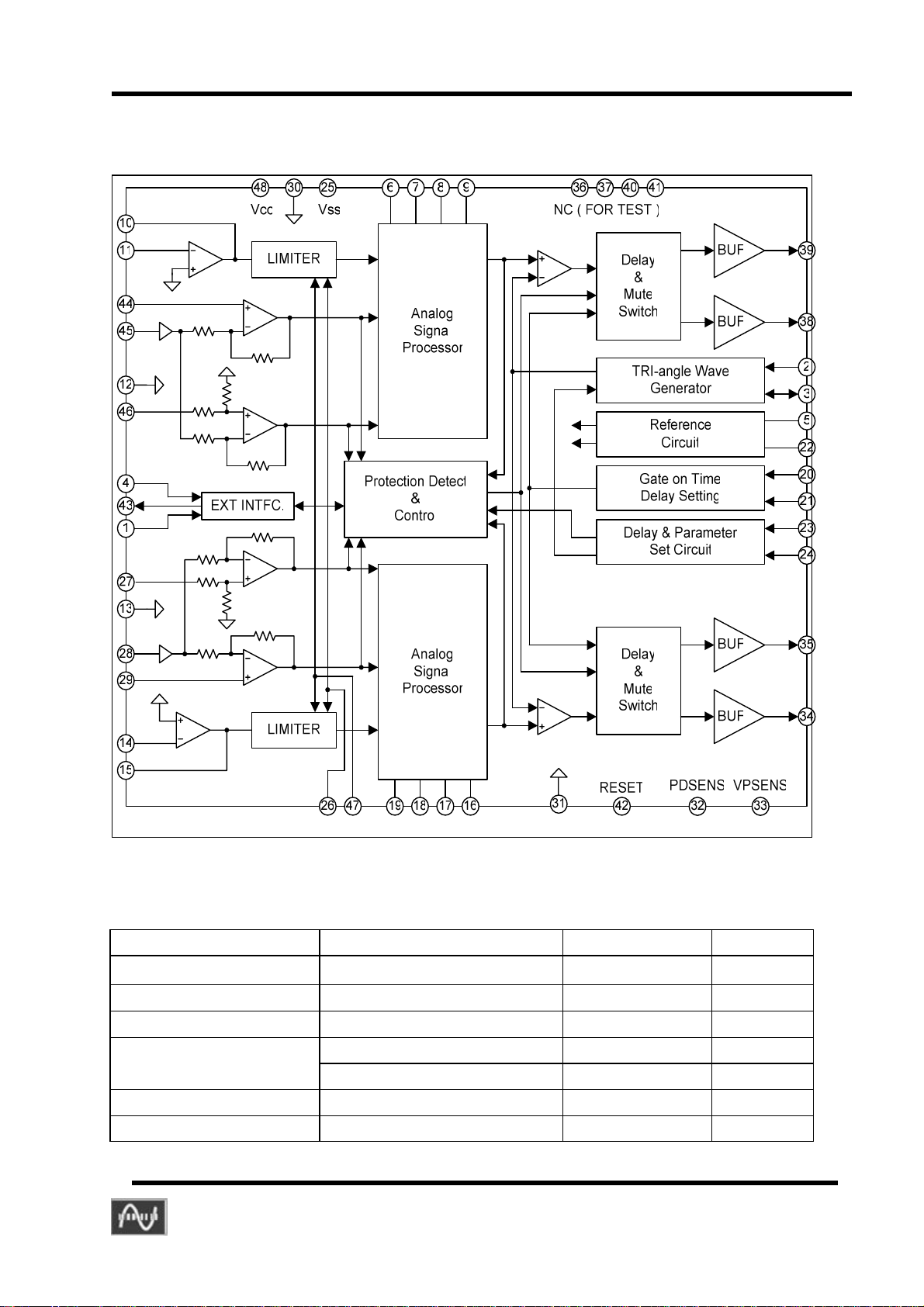
2. BLOCK DIAGRAM
3 ABSOLUTE MAXIMUM RATINGS
Symbol Parameter Value Units
VCC, VSS
Tstg Storage Temperature –55 to 150
Topr Operating Temperature –25 to 75
Electro-Static Discharge Human Body Model, All pin 2000 V
Electric Over Stress All pin 16 V
Pd Power Dissipation 1000 mW
Digital & Analog Co., Ltd. (Rev. 1.0) -4-
Driver supply voltage
Machine Model, All pin 200 V
± 7.5
V
°C
°C
S1A0071 Audio Processor for Class-D Power AMP
4. PIN DESCRIPTION
NO. Name I/O Description
1 OPT I
2 OSCEN I Triangle wave generator enable input
3 SIO B Triangle wave I/O
4
5 VD O Logic power supply pin (internal generated)
6,7,8,9 CX_L B L-channel amp capacitor connected pin for Phase & gain
10 VO_L O L-channel pre-amp output pin for gain setting
11 VIN_L I L-channel pre-amp input pin
12 GND_A P L-channel sound ground
13 GND_A P R-channel sound ground
14 VIN_R I R-channel pre-amp input pin
15 VO_R O R-channel pre-amp output pin for gain setting
16,17,18,19 CX_R B R-channel amp capacitor connected pin for Phase & gain
20 PDCTR I P-MOS gate delay setting pin
21 NDCTR I N-MOS gate delay setting pin
22 VB O Regulated voltage output pin for internal current bias
23 VC I Triangle wave magnitude setting input
24 CDLY I Time delay capacitor pin for internal use
25 VSS P Negative power supply pin
26 VLN I Soft clipping low level input
27 CF2_R I R-channel current feed back input 2
28 CF1_R I R-channel current feed back input 1
29 VF_R I R-channel voltage feed back input
30 GND_CH P Control block ground
31 GND_A P Reference block ground
32 PDSENS I Power Down Detection
33 VPSE NS I The operating voltage detec tion pin of the exter na l
34 NO_R O R-channel N-MOS switching output (PWM)
35 PO_R O R-channel P-MOS switching output (PWM)
36 NS3 - NC (Test pin for evaluation)
37 NS2 - NC (Test pin for evaluation)
38 PO_L O L-channel P-MOS switching output (PWM)
39 NO_L O L-channel N-MOS switching output (PWM)
MUΤΕ
Active high. If it is h igh, PW M out put is ac tivat ed after power
ON Mute Time, T
I Mute control input. It is also used for external protection.
Active low. Low state is muted state.
MOSFET. When its function is not used, this pin must be
tied to VCC and about 0.1uF is connected to GND
. Otherwise (Default = HIGH)
M
Digital & Analog Co., Ltd. (Rev. 1.0) -5-
S1A0071 Audio Processor for Class-D Power AMP
PIN DESCRIPTION (CONTINUED)
NO. Name I/O Description
40 NS1 - NC (Test pin for evaluation)
41 NS0 - NC (Test pin for evaluation)
42
43
44 VF_L I L-channel voltage feed back input
45 CF2_L I L-channel current feed back input 2
46 CF1_L I L-channel current feed back input 1
47 VLP I Soft clipping high level input
48 VCC P Positive power supply pin
* I: Input, O: Output, B: Bi-directional, P: Power Supply, -: No Connection.
RESET
PMON
I Logic reset input
O Protection monitor output
Digital & Analog Co., Ltd. (Rev. 1.0) -6-

S1A0071 Audio Processor for Class-D Power AMP
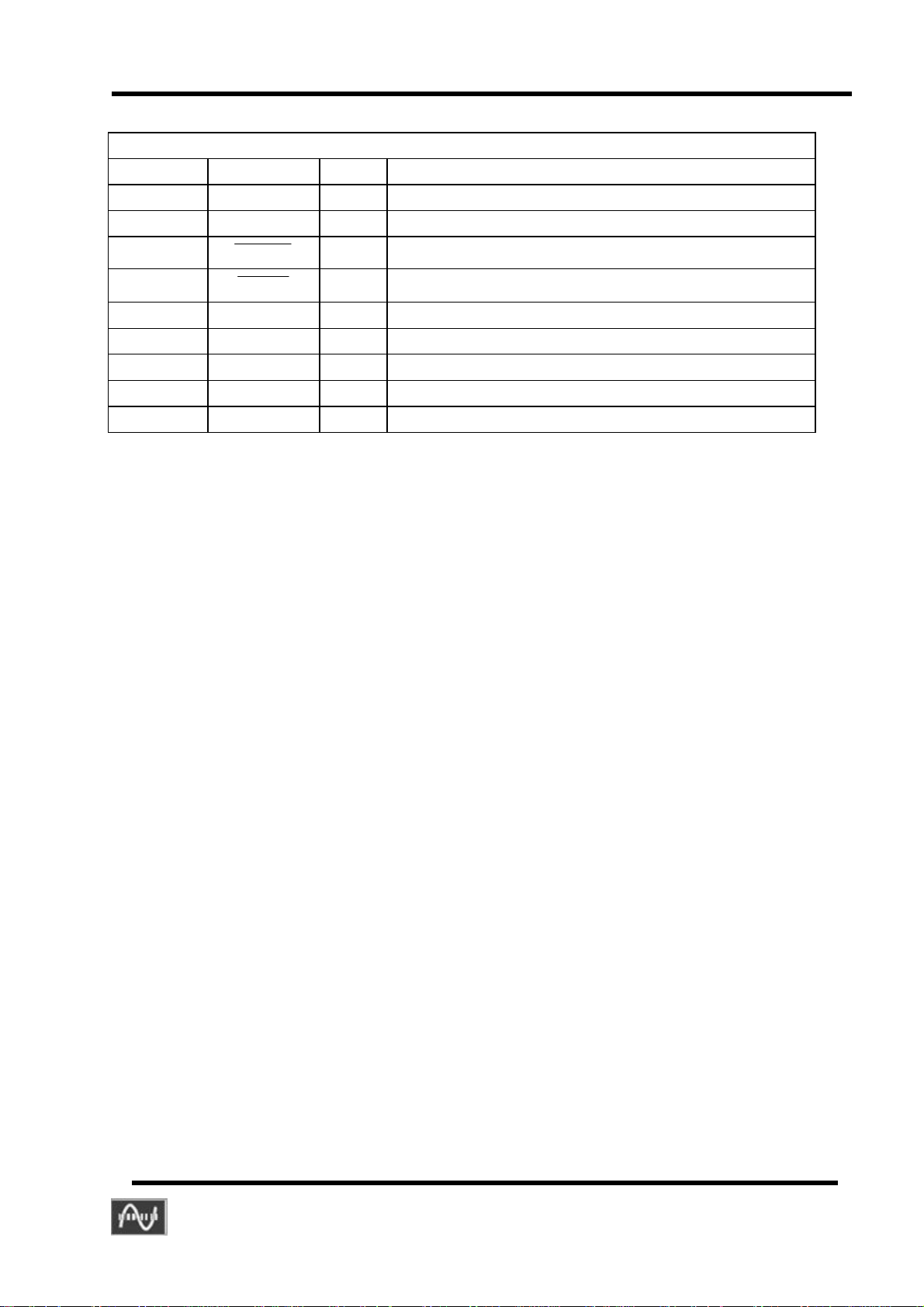
5. ELECTRIC CHARATERISTICS
ELECTRICAL CHARACTERISTICS
Ta = 25°C, Vi = 0.3Vrms, f = 1kHz, VCC = 5V, VSS = -5V, R
Vc = 1.0V, Power Supply Voltage (VCCP, VSSP) = ± 30V
Characteristic Symbol Condition Value Unit
Supply current Icc Vi = 0
Driver rising time Tr CL = 10pF
Driver falling time Tf CL = 10pf
PGATE on time delay Tdp CL = 10pf
NGATE on time delay Tdn CL = 10pf
Driver low level Vgl Isink = 100uA, DC - -4.5 -4.0 V
Driver high level Vgh Ipush = 100uA, DC -1.0 -0.5 - V
= 1.5V, VLN = -1.5V
Input limiting voltage Vlim
Oscillation frequency Fosc - 360 450 540 kHz
Oscillation level Vosc Vc = 1.0V 2.0 2.2 2.4 Vp-p
OSCEN conversion voltage Vto - 1.0 1.5 2.2 V
MUΤΕ conversion volta ge
Vtm - 1.2 1.6 2.0 V
V
LP
= 4Ω,
L
Min. Typ. Max.
2.8 3.0 3.2 Vp-p
35
20
20
20
20
mA
nsec
nsec
nsec
nsec
PMON "L" level
Circuit bias voltage Vb - 2.8 3.0 3.2 V
Logic supply voltage Vd - -1.2 -0.8 -0.2 V
Audio amp gain Gp1 f = 1kHz.closed loop -0.5 -2.5 -4.5 dB
Total voltage gain Gv Vi = 0.1Vrms, f = 1kHz 24.0 26.0 28.0 dB
Channel balance CB Vi = 0.1Vrms, f = 1kHz -1.0 0 1.0 dB
Ripple rejection ratio RR Vr = 0.2Vp-p, f = 120Hz - - -70 dB
Output offset voltage Vofs Vi = 0 - - 0.1 V
Maximum output Pomax1
Total harmonic distortion THD1 Po = 10W, RL = 4ohm - 0.030
Output noise voltage Vno Vi = 0 0Vrms - 160
Channel cross talk CT Vi = 0.3Vrms - - -80 dB
Mute damp ratio Rmute Vi = 0.8Vrms - - -110 dB
Over current detect voltage Voc - 0.70 0.96 1.20
Vpmon
Gp2 f = 450kHz, open loop 9.0 12.0 15.0 dB
Pomax2
THD2 Po = 50W, RL = 4ohm - 0.062
THD3 Po = 5.0W, RL = 8ohm - 0.025
THD4 Po = 25W ,RL = 8ohm - 0.026
Rmon = 470Ω
THD = 1%, R
THD = 1%, R
= 4hm
L
= 8ohm
L
- - 0.4 V
75.2
43.5
W
W
%
%
%
%
uVrms
± V
Digital & Analog Co., Ltd. (Rev. 1.0) -7-

S1A0071 Audio Processor for Class-D Power AMP
6. Typical Performance
±30V
±25V
±35V
Drivers Power Supply Voltage & Out Pow
±40V ±45V
±VCCP = ±25V
±Vcc = ±5V
f = 1kHz
BW = 22Hz~ 20kHz
R
= 4Ω
L
AES 17FILTER
±VCCP = ±30V
±Vcc = ±5V
f = 1kHz
BW = 22Hz~ 20kHz
R
= 4Ω
L
AES 17FILTER
±VCCP = ±35V
±Vcc = ±5V
f =1kHz
BW = 22Hz~ 20kHz
R
=4Ω
L
AES 17FILTER
±VCCP = ±40V
±Vcc = ±5V
f =1kHz
BW = 22Hz~ 20kHz
R
=4Ω
L
AES 17FILTER
±VCCP = ±45V
±Vcc = ±5V
f = 1kHz
BW = 22Hz~ 20kHz
R
= 4Ω
L
AES 17FILTER
From the above m eas ur e data, the us er c an make an audio am plif ier system with S1A00 71 f or several
conditions. For ex ample, if user want to m ake a class D type audio am plifier wit h specification like as
0.1% 50W system and load impedance 4Ω. User just setup the power supply and sm all quality of
resistor and capacitor, FET drive and FET switch f or thi s , and you can make a 0.1% 50W 2Channel as
faster and easily. If you want to make a audio amplifier lik e as THD+N <1%, 200W 2Channel system,
user can get the system quickly. Also user can make a 5.1Channel with S1A0071 3EA as easily.
Digital & Analog Co., Ltd. (Rev. 1.0) -8-

S1A0071 Audio Processor for Class-D Power AMP
Typical Performance
±VCCP = ±25V
±Vcc = ±5V
f = 1kHz
BW = 22Hz ~
R
L
AES 17FILTER
20kHz
= 4Ω
±VCCP = ±25V
±Vcc = ±5V
f = 1kHz
BW = 22Hz
R
=8Ω
L
AES 17FILTER
20kHz
±VCCP = ±25V
±Vcc = ±5V
Po = 1W
BW = 22Hz ~
R
L
22kHz
= 4Ω
±VCCP = ±25V
±Vcc = ±5V
Po =1W
BW = 22Hz
R
=8Ω
L
22kHz
Digital & Analog Co., Ltd. (Rev. 1.0) -9-

S1A0071 Audio Processor for Class-D Power AMP
Ω
Typical Performance
±VCCP = ±25V
±Vcc = ±5V
Po = 10W
R
= 4Ω
L
BW = 22Hz ~ 30KHz
BW = 22Hz ~ 22KHz
±VCCP = ±25V
±Vcc = ±5V
Po =5W
R
=8
BW = 22Hz ~ 30KHz
BW = 22Hz ~ 22KHz
±VCCP = ±25V
±Vcc = ±5V
Po = 10W
19kHz, 20kHz 1 : 1
BW = 22Hz ~
0dBr = 17V
R
L
22kHz
= 4Ω
±VCCP = ±25V
±Vcc = ±5V
Po =5W
19kHz, 20kHz 1 : 1
BW = 22Hz ~
22kHz
Digital & Analog Co., Ltd. (Rev. 1.0) -10-

S1A0071 Audio Processor for Class-D Power AMP
Typical Performance
±VCCP = ±25V
±Vcc = ±5V
Po = 1W
f = 1kHz
BW = 22Hz ~
0dBr = 17V
R
L
22kHz
= 4Ω
±VCCP = ±25V
±Vcc = ±5V
Po = 10W
f = 1kHz
BW = 22Hz ~
0dBr = 17V
R
L
22kHz
=4Ω
±VCCP = ±25V
±Vcc = ±5V
Po = 1W
f = 1kHz
BW = 22Hz~ 22kHz
0dBr = 17V
R
L
=
8Ω
±VCCP = ±25V
±Vcc = ±5V
Po =5W
f = 1kHz
BW = 22Hz~ 22kHz
0dBr = 17V
R
L
=
8Ω
Digital & Analog Co., Ltd. (Rev. 1.0) -11-

S1A0071 Audio Processor for Class-D Power AMP
Typical Performance
±VCCP = ±25V
±Vcc = ±5V
Po = 0W
BW = 22Hz~ 22kHz
0dBr = 17V
R
= 4Ω
L
±VCCP = ±25V
±Vcc = ±5V
BW = 22Hz~ 22kHz
0dBr = 17V
Po = 5W, RL = 8Ω
Po = 10W, RL = 4Ω
RL = 8Ω
RL = 4Ω
±VCCP = ±25V
±Vcc = ±5V
AES 17FILTER
THD+N < 10%
±VCCP=±25V
±Vcc =±5V
Po = 0W
BW = 22Hz~22kHz
R
=4Ω
L
PSRR -
PSRR +
Digital & Analog Co., Ltd. (Rev. 1.0) -12-

S1A0071 Audio Processor for Class-D Power AMP
7. TEST CIRCUIT
Digital & Analog Co., Ltd. (Rev. 1.0) -13-

S1A0071 Audio Processor for Class-D Power AMP
8. APPLICATION CIRCUIT
Digital & Analog Co., Ltd. (Rev. 1.0) -14-

S1A0071 Audio Processor for Class-D Power AMP
9. APPLICATION NOTE
Note 1
The OPT [Active high] contr ols the power on mute f unction [referred to N ote 7]. User can preve nt the
unstable operation b y using this pin and use can use th is signal to prevent the POP noise dur ing the
power-on time.
Note 2
The OSCEN pin controls the direction of OSC pin because OSC has a bidirectional operation. The
S1A0071 has a built-in triangle oscillator, so user can selectable to use the internal oscillator or
external oscillator. If user wants to interna l oscillator, the OSCEN pin connects to VCC then O SC is
output port and used to detect the int ernal oscill ation wavef orm. If user wan t to mak e an amplifier with
three or more channels s et, at this cas e, user m use be careful to m ake a s ystem, special ly the setting
of oscillator frequency, because when user can use the each independent internal oscillators
configuration, the system can be generated from mixed modulation resulting from the frequency
deviation between osc illators in each chip, resp ectively. In such case, the oscillator in one of the IC’s
must be MASTER, shared with the other IC’s oscillato r signal, and t he oscillator in the other IC’s m ust
disabled by the use of the OSCEN pin (SLAVE mode). Then, the OSCEN pin of MASTER ICs is
connected to VCC (or Open) and the OSCE N pin of the other IC (Slaves) mus t be grounded (GND),
and the SIO pins mus t be connected to each other. As you can see the Figure 1 , the oscillator signa l
of the MASTER IC provides the triangle wave to the Slave ICs.
VCC
IC1
OSCEN
SIO
OSCEN
IC4
IC3
SIO
OSCEN
SIO
Figure 1. Multi Chip Application
Note 3
MUΤΕ Pin controls the switching operation of MOSFET [Active Low]. When Mute Pi n is low, the
PO_R, NO_R, PO_R and NO _R signal g o to lo w leve l so the MO SFET operation is s top. Sound is not
heard any more. T his operation can be use as protection cond ition. So
MUΤΕ
pin is also used for
external protection. S1A0071 has internal protection circuit. However, if user w ant to add a special
protection circuit to the set, the output of the added circuit which is active low is directed to the
MUΤΕ
pin (PIN4), which then stops the buffer output.
Digital & Analog Co., Ltd. (Rev. 1.0) -15-

S1A0071 Audio Processor for Class-D Power AMP
R
Note 4
The internal gain of S1A0071 is 26dB. (Condition: R1 = R2)
When user wants to get a high gain system, User can do this by changing the values of R1 and R2.
In this case, the Total Gain can be obtained as follows:
2
20)( +×=
R
LogdBGAINtotal
26
1
If the values of R1 and R2 are very high, it will exp ect the DC offset and if the values of R1 and R 2 are
very low, then the THD+N value is high on high power system. By an appropriate R1 and R2 selection,
you can minimize the DC offset and get the good the THD+N characteristics.
Note 5
In the application circu it, the resistor Rp connected to the PDCTR and the resistor Rn connected to
NDCTR pins. User can adj ust these resistors values to c ontrol the ON tim e delays of P-MOSFET and
N-MOSFET. Because there is a turn-on delay tim e and rising t ime and fal ling time, turn- off delay tim e
of each MOSFET drive, so user must set the on time dela y for each P-MOSFET and N-MOSFET to
prevent arm-shor t s ituati on. A ls o more important, the R p a nd Rn selection aff ec t the s ou nd qu al it y a nd
amplifier efficiency, so user should be select appropriate value.
Designed rule of S1A 0071, the gate off tim e minimized and the ON time can be variable so that user
can set the overlap time external ly. The PDCTR pin and NDCTR pin voltages ar e generall y set to that
of VB (pin 22) and the flowing current, controlled by the values of Rp and Rn connected externally, can
be used to delay the intern al gate ON tim e. The rec ommended cur rent range is 10Kohm to 200Kohm ,
from which one can select the appropriate current according to the selected output MOSFET and
circuit configuration.
As the resistances inc reas e , O N time is further d elayed. Rp and Rn can s et t he ON time dela ys of PMOSFET and N-MOSFET, respectively.
Tdpo Tdno Tdpo Tdno
PMOS Gate Drive
Output (PO)
NMOS Gate Drive
Output(NO)
Figure 2. Gate Driver on Time Delay
Digital & Analog Co., Ltd. (Rev. 1.0) -16-

S1A0071 Audio Processor for Class-D Power AMP
Rp,Rn & Dead-Time
160
140
120
100
80
60
Dead-Time[nS]
40
20
0
40 60 80 100 120 140 160 180 200 220 240
Rp&Rn (kΩ)
Note 6
The Vc ( DC Voltage of carrier frequency) sets the oscillation level of the triangle oscillator. The
internal oscillation f requency is s et to about 450k Hz, independe nt of the oscilla tion level, an important
factor that sets the conversion ga in f r om the internal comparator to the speaker. Based on the input Vc,
the oscillation level is set to approximately ± Vc (Vp-p), and can be monitored at the SIO (Pin3).
It is acceptable to m ake Vc voltage from the ex ter na l vo ltage source; however, we recommend making
the Vc voltage from the regulated voltage VB (Pin22) divided b y Ra and Rb. If Vc is used with the
capacitor to prevent noise input, a circuit with better characteristics can be configured.
VVC
To get the high THD characteristics, the gain of S1A0071 is designed as 26dB and the application
circuit use the
amplifier gain, so if user want to get the high power and increase the main power, then user must
re-setup the Vc values. We recommended as below value for user's application.
± 30V for main power and the 0.8V for Vc. The ratio of main power divide Vc relate a
VCCP, VSSP
=
PP
−
2
)(
RbVB
××
: VB = 3.05V with VCC = 5V, VSS = -5V
)(
RbRa
+
± 20V ± 30V ± 45V
Ra
Rb
22KΩ 22KΩ 22KΩ
5.6KΩ 8.2KΩ 15KΩ
Digital & Analog Co., Ltd. (Rev. 1.0) -17-

S1A0071 Audio Processor for Class-D Power AMP
×
Note 7
When power is turned on, the circuit operates unstably, possibly generating noise. To prevent
this unstable situation, the S1A0071 use the CDLY pin (pin# 24), which can be connected to a
capacitor. This CDLY pin used to generate a slight time delay from power up to when the
circuit starts to operate normally. The CDLY pin drive’s capacity is about 1.0㎂ and the mute
mode sustains until the externally connected capacitor charges to a voltage equal about VB
(pin 22). The time delay can be calculated as follows:
CVC
×
Tdly ×≅+
= 60.3
(sec)
Ta
I
is the internal processing time that used in the removal of circuit settling time and other
T
a
pop noises. Tdly also decides the protection restart time. Among the protection functions in
S1A0071, those that remove "causes" (Thermal Protection, Over Current Protection) oscillate
from normal operation → protection → normal operation → protection → … , generating
very fast blocking oscillation. The Tdly decides (delays) the repeat cycle of the oscillation,
which protects the circuit and controls unstable operations. Those protection functions
(Output DC Short) that do not remove "causes" are not affected by Tdly, and once the cause
has been removed, they return to normal operation.
Note 8
S1A0071 has a built-in limiting block at the input stage that remove noise signal that may be
generated by discontinuous feedback and also this limit block operate as a clipping circuit due
to over-input signal. When a specific voltage (± Vls) is applied to VLP and VLN, the soft
clipping function starts to operate on the input whose value lie outside the ± Vls range, on the
C
3
=+
0.1
μ
CETa
(Ta « Tdly)
basis of the Pre Amp output with its gain set by R1 and R2. As a result, the entire circuit is
enabled to drive only the signals that lie within the operating range, thus maintaining a
continuous feedback loop which allows the circuit to output a soft clipped output waveform
even for an input lying outside the output dynamic range.
Vls must be set differently according to the MOSFET power supply voltage and power supply
impedance, and MOSFET ON resistance. If we assume that the power supply impedance is
ideal (= 0) and MOSFET ON resistor is ideal (0 Ohm), the appropriate values for Vls values on
the power supply voltage (VCCP, VSSP) would be as follows:
VCCP, VSSP
Vls
± 20V ± 30V ± 45V
± 1.05V ± 1.43V ± 2.15V
Digital & Analog Co., Ltd. (Rev. 1.0) -18-

S1A0071 Audio Processor for Class-D Power AMP
(This value is obtained by dividing MOSFET power supp ly voltage with Rx and Ry. Considering the
speaker load resistance and power supply impedance, Vls (soft clipping level) is generated. So,
VLN/VLP accepts this value, and then stable operation is expected.)
To decide on the actually appropriate Vls, you m ust monitor the ou tput wavef orm at the set conn ected
to the power suppl y. You can set Rx and Ry to values that wil l make VLP and VLN gen er ate maximum
waveforms, respec tively; within the range t hat has no clipping dis tortion and ot her noises. If you don't
want to operate the soft clipping function, connect VLN and VLP pins to VCC and VSS.
※ Other Application information
♦ PROTECTION
S1A0071 has built-in Output DC Short Protection, and Over Current Protection. When the
protection block output pins are shorted to VCCP or GND or VSSP, respectively, the internal
detect circuit immediately stops the buffer output.
The Over Current Detect function is driven by the Current Sensing resistor (50m ), which
indicates an over current if the resistor develops a potential of about 1.0V. Then the current is
about 1.0(V) / 0.05 ( ) = 20 (A). If the speaker " -" pin becomes VCCP or VSSP and DC shorted,
the sensing resistor will be destroyed as well as S1A0071. To prevent IC destruction, you can
insert resistors of few k in series at the CF1 pins (Pin28, 45). (Please refer to No te 5 for more
details on protection return time)
♦ FET DRIVER
S1A0071 produces an output of 4.5Vp-p and low level is VSS. Any GATE BUFFER ICs can satisfy
these conditions, but they should be designed as FAIR to optimally use with S1A0051, a MOSFET
DRIVER
Digital & Analog Co., Ltd. (Rev. 1.0) -19-

S1A0071 Audio Processor for Class-D Power AMP
10. PACKAGE DIMENSIONS
0.05
MIN
0.002
1.00
+ 0.05
0.039
+ 0.002
#1 #48
0.50
0.020
+ 0.07
- 0.03
+ 0.003
- 0.001
0.20
12.50 + 0.10
0.492 + 0.004
0.0078
TYP
0.50
0.020
#24 #25
1.20
MAX
0.047
0.60
0.024
+ 0.07
- 0.03
0.127
+0.15
-0.10
+0.006
-0.004
+ 0.003
0.005
- 0.001
6.10
0.240
0.319
8.10
+ 0.10
+
0.004
Digital & Analog Co., Ltd. (Rev. 1.0) -20-
 Loading...