

S1A0051 FET Driver for Class-D PWM Amp
Data Sheet
(Rev. 1.0)
for S1A0051
FET Driver
For Class-D PWM Amp
Digital & Analog Co., Ltd.
Digital & Analog Co., Ltd. (Rev. 1.0) -1-

S1A0051 FET Driver for Class-D PWM Amp
CONTENT
1. INTRODUCTION.................................................................................3
2. BLOCK DIAGRAM .............................................................................3
3 ABSOLUTE MAXIMUM RATINGS ......................................................3
4. PIN DESCRIPTION.............................................................................4
5. ELECTRIC CHARATERISTICS..........................................................4
6. FUCTIONAL DESCRIPTION..............................................................5
7. TEST CIRCUIT ...................................................................................6
8. APPLICATION CIRCUIT.....................................................................7
8. APPLICATION CIRCUIT.....................................................................7
9. PACKAGE DIMENSIONS...................................................................8
Digital & Analog Co., Ltd. (Rev. 1.0) -2-

S1A0051 FET Driver for Class-D PWM Amp
1. INTRODUCTION
◎ FET (GATE) Driver for CLASS-D Amp
◎ Schmitt Triggered Input
◎ Totem-Pole Str uct ured O utput Stage
◎ Four Independent Power MOSFET Gate Drivers
◎ Operating Voltage : 10 ~ 12V (Single Power), ± 5.0V – ± 6.0V(Dual Power)
◎ High Performance for Switching Characteristics
○ Typically 15ns for rising/falling time with 1nF load
○ Typically 20ns for propagation delay time with 1nF load
◎ BiCMOS Technology / 16 ETSSOP
2. BLOCK DIAGRAM
1
2
NC
3
4
5
6
7
NC
VCC
Reference &
Logic Power
Supp lier
VSS VCC34
8 9
3 ABSOLUTE MAXIMUM RATINGS
Symbol Parameter Value Units
VCC Driver supply voltage 13.5 V
Tstg Storage Temperature -40 – 125
Topr Operating Temperature -25 – 75
Human Body Model, All pin 2000 V Electro-Static
Discharge
Pd Power Dissipation 1000 mW
Machine Model, All pin 200 V
16
VCC12
Driver1 15
Driver2 14
VSS12
1/2 Bias
VSS34
Driver3
Driver4
13
12
11
10
°C
°C
Digital & Analog Co., Ltd. (Rev. 1.0) -3-

S1A0051 FET Driver for Class-D PWM Amp
4. PIN DESCRIPTION
NO. Name I/O Description
1 VCC P Positive power supply pin
2 NC - No Connected
3 VI1 I Logic Driver Input 1
4 VI2 I Logic Driver Input 2
5 VI3 I Logic Driver Input 3
6 VI4 I Logic Driver Input 4
7 NC - No Connected
8 VSS P Negative power supply pin
9 VCC34 P Positive power supply pin for driver 3, 4
10 VO4 O Logic Driver Output 4
11 VO3 O Logic Driver Output 3
12 VSS34 P Negative power supply pin for driver 3, 4
13 VSS12 P Negative power supply pin for driver 1, 2
14 VO2 O Logic Driver Output 2
15 VO1 O Logic Driver Output 1
16 VCC12 P Positive power supply pin for driver 1, 2
* I: Input, O: Output, B: Bi-directional, P: Power Supply, -: No Connection.
5. ELECTRIC CHARATERISTICS
With no special mentions, Ta = 25°C, VCC = 10V
Characteristic Symbol Condition Value Unit
Min. Typ. Max.
Supply Current ICC1 VCC = 10V
All input pin is Low State
ICC2 VCC = 12V
All input pin is Low State
Switching Characteristics
Output Rising Time Tr CL=1nF - 15 80 nsec
Output Falling Time Tf CL=1nF - 15 80 nsec
Propagation Delay Td CL=1nF - 20 50 nsec
Driving Characteristics
Output High Level VOH Ipull = 5mA 9.0 9.25 9.5 V
Output Low Level VOL Ipush = 5mA - - 0.4 V
Input Threshold
High State Logic 1 VIH - 3.3 - - V
Low State Logic 0 VIL - - - 0.5 V
1 3 5 mA
1.5 3.7 6.0 mA
Digital & Analog Co., Ltd. (Rev. 1.0) -4-

S1A0051 FET Driver for Class-D PWM Amp
6. FUCTIONAL DESCRIPTION
Please refer to notes on S1A0071 for more details on the Class-D Amp.
S1A0051 can be used not only in one power supply mode(+10V ~ +12V) but also in dual power
supply mode( ±5V ~ ±6V ). It can rec eive input s ignals thr ough the Schmitt Trigger, and has a bui lt-in
logic power suppl y, which m akes the logic level independ ent of the input level when t he input signal
level is different from the output signal level. S1A0051 drives inputs and outputs that have a noninverse relation S1A 0051 drives each out put that have a non- inverse relation about each input and it
has superior short propagation delay and fast rising/falling timing characteristics.
Input Interface (Schmitt Trigger)
In S1A0051, the built- in logic power supply sets the internal logic operating voltage, and the po wer
supply voltage range is 5.0V 0.5V for dual power supply mode. By interfacing with the Schmitt
Trigger with a hysteresis, the input is unaffected by noise.
Driver & 1/2 BIAS
Configured as CMOS, excluding totem pole output stage, to enhance switching characteristics, the
driver generates the center operating voltage (1/2 BIAS) to prevent MOS breakdown when the process
CMOS breakdown voltage BVgs is 8V. S1A0051's in put/output relationship is non-inver ted, which is
shown in the timing diagram in Figure. 1.
Input
Td
90% 90%
Output
10%
Figure 1. Input vs. Output Timing Diagram
Tr
10%
Tf
Digital & Analog Co., Ltd. (Rev. 1.0) -5-

S1A0051 FET Driver for Class-D PWM Amp
7. TEST CIRCUIT
VCC
VCC12
VCC34
VCC
100u
GND12
GND34
GND
VCC
2K
VS
S1
S2
S3
S3
S4
100K
100K
VCC
100K
VCC
NC
VI1
VI2
VI3
VI4
NC
100K
VSS VCC34
S1A0051X
16 ETSSOP
VCC12
VO1
VO2
VSS12
VSS34
VO3
VO4
1n
1n
1n
1n
VCC12
S5
S6
GND12
GND34
S7
S8
VCC34
S9
TP
S10
2K
Digital & Analog Co., Ltd. (Rev. 1.0) -6-
S1A0051 FET Driver for Class-D PWM Amp
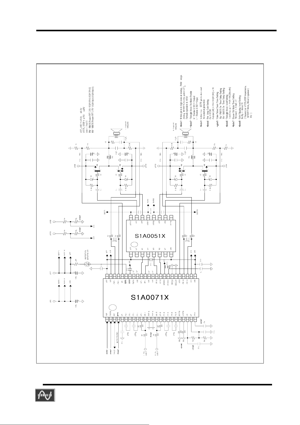
8. APPLICATION CIRCUIT (refer to S1A0071 datasheet)
Digital & Analog Co., Ltd. (Rev. 1.0) -7-

S1A0051 FET Driver for Class-D PWM Amp
9. PACKAGE DIMENSIONS
Dimension in Milimeters / Inches
TOP VIEW
+ 0.07
- 0.03
0.127
#1
#8 #9
4.40 + 0.10
- 0.00 1
+ 0.003
0.005
0.173 + 0.004
6.4 + 0.15
#16
5.0 + 0.1
0.197 + 0.004
MAX 1.2
0.0472
0.9
0.0354
0.245 + 0.055
0.009 + 0.0020.65
0.0256
+0.10
0.60
BOTTOM VIEW
-0.10
-0.004
+0.004
0.024
#8
#1 #16
0.252 + 0.006
MAX 3.0
MAX 0.118
#9
MAX 3.0
MAX 0.118
Digital & Analog Co., Ltd. (Rev. 1.0) -8-
 Loading...