

Calogic LLC SD5501N Datasheet
CORPORATION
N-Channel Depletion-Mode
4-Channel DMOS FET Array
SD5501
FEATURES
Normally ON Configuration
••
Low Interelectrode Capacitances
••
High-Speed Switching
••
Wide Dynamic Range
••
APPLICATIONS
High-Spe ed A n al og Sw itch e s
••
Wide-Ba nd Dual Di ff ere ntia l Amp lifi ers
••
Dual Cascode Amplifiers
••
High Inter cept Point Doubl e Bala n ced Mi xer s
••
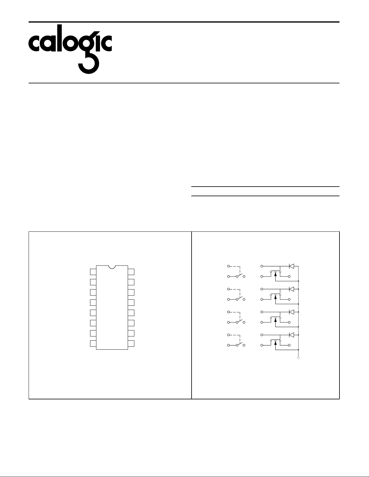
PIN CONFIGU R ATI O N
1
CD2
D1
BODY
G1
S1
S2
G2
N/C
D2
2
3
4
5
6
7
8
TOP VIEW
16
15
14
13
12
11
10
9
D4
N/C
G4
S4
S3
G3
N/C
D3
DESCRIPTION
The SD5501 is manufactured utilizing Calogic’s proprietary
high speed, low capacitance DMOS process featuring an
N-Channel depletion-mode design. This "normally-ON"
device is well suited for high speed instrumentation and
communication systems where multiple channels are required
for fast switching or dual amplification. Available in a 16-pin
plastic dual in-line plast ic pack age or chip for m .
ORDERING INFORMATION
Part Package Temperature Range
o
SD5501N Plastic -55
XSD5501 Sorted Chips in Carriers -55
C to +125oC
o
C to +125oC
SCHEMA TIC DIAGRAM
G
3
1
6
8
11
9
14
16
3
S
4
5
12
13
D
1
6
D
8
11
D
9
14
D
16
4
G
S
5
G
S
12
G
S
13
2
BODY
SD5501
ABSOLUTE MAXIMUM RATINGS (TA = +25oC unless otherwise note d)
Drain-Sour ce Voltage. . . . . . . . . . . . . . . . . . . . +30 Vdc
V
DS
V
Source-Drain Volt age. . . . . . . . . . . . . . . . . . . . +0. 5 Vdc
SD
Drain-Body Volt age . . . . . . . . . . . . . . . . . . . . . . +30 Vdc
V
DB
Source-Bod y Voltage. . . . . . . . . . . . . . . . . . . . . +15 Vdc
V
SB
V
Gate-Source Volt age. . . . . . . . . . . . . . . . . . . . . +25 Vdc
GS
Gate-Body Voltage. . . . . . . . . . . . . . . . . . . . . . . +25 Vdc
V
GB
Gate-Body V olt age. . . . . . . . . . . . . . . . . . . . . . -0.3 Vdc
V
Gate-Drain V o ltag e . . . . . . . . . . . . . . . . . . . . . . +25 Vdc
GD
Continuous Drain Curren t . . . . . . . . . . . . . . . . . . 50 mA
I
D
P
D
P
D
T
j
T
S
CORPORATION
Total Package Power Dissipat ion
(at or below TA = +25
Linear Derating Fac tor. . . . . . . . . . . . . . . . 10.7 mW/
Single Device Power Dissipation
(at or below TA = +25
Linear Derating Facto r. . . . . . . . . . . . . . . . . 5.0 mW/
o
C) . . . . . . . . . . . . . . . . . 640 m W
o
C) . . . . . . . . . . . . . . . . . 300 m W
o
o
Operating Junction Temperature Range . . -55 to +85oC
Storage Temperature Range . . . . . . . . . -55 to + 150oC
C
C
ELECTRICAL CHARACTERISTCI S (T
= +25oC unless otherwise noted)
A
SYMBOL CHARACTERISTIC MIN TYP MAX UNITS TEST CONDITIONS
STATIC
B
VDS
B
VSD
B
VDB
B
VSB
I
GSS(fwd)
I
G
V
GS (off)
V
GS (on)
I
DSX
r
DS (ON)
Drain-Source Breakdown Voltage 20
Source-Drain Breakdown Voltage 10 IS = 10 nA, VGD = VBD = -5.6V
Drain-Body Breakdown Voltage 25 ID = 10nA, VGB = 0, Source Open
Source-Bod y Breakdown Voltage 15 IS = 10µA, VGB = 0, Drain Open
Forward Gate Leakage Current 1.0 nA VGS = 25V, VDS = VBS = 0
Gate Operating Current
-3.0 -100 pA
-0.7 -10 nA T
Gate - Source Cutoff Voltage -1.0 -5.0
Gate-Source On Voltage -0.3 -3.0 VDG = 10V, ID = 5mA, VSB = -5.6V
Zero Gate Voltage Drain Current
7.0 40
5.0 T
Drain-Source On Resistance 100 150 ohms ID = 1.0mA, VGS = 0, VBS = -5.6V
ID = 10 nA, VGS = VBS = -5.6V
V
V
= 15V, ID = 5. 0 mA,
DG
V
= -5.6V
BS
VDS = 10V, ID = 1.0µA, VBS = 5.6V
V
V
= 10V, VGS = 0,
mA
DS
V
BS
= -5.6V
DYNAMIC
g
fs
g
os
C
iss
C
oss
C
rss
C
(gs + sb)
Common-Source Forward Transconductance
Common-Source Output Conductance 200 350 µS
Common-Source Input Capacitance 3.5
Common-Source Output Capacitance 1.2
Common-Source Reverse Transfer Capacitance 0.3
Source Node Capacitance 4.5
(1)
6.0 7.5 12 mS
V
= 10V
DG
I
= 5.0 mA
D
V
= -5.6V
pF f = 1 MHz
BS
MATCHING
V
GSM
r
DS(on)
I
DXSM
g
fsm
Gate Source Voltage Match 50 mV VDG = 10V, ID = 5.0mA, VBS = -5.6V
Drain-Source On Resistance Match 10% ID = 1.0 mA, VGS = 0, VBS = 5.6V
Zero Gate Voltage Drain Current Mat ch 10%
Transconductance Match
(1), (2)
10% f = 1 KHz
V
= 10V, ID = 5. 0 mA,
DG
V
= -5.6V
BS
Note 1: Pulse Test , 80 sec, 1% Duty Cycle
Note 2: Match of 4 channels
= +1 25oC
A
= +1 25oC
A
f = 1 KHz
 Loading...