

Calogic LLC SD404CY, SD404BD Datasheet

CORPORATION
High Speed DMOS
N-Channel Switch
SD404
FEATURES
High Speed Switching. . . . . . . . . . . . . . . . . . . . . tr < 2ns
••
Low Capaci t a nce . . . . . . . . . . . . . . . . . . c
••
Ver y Low o n Re si st ance. . . . . . . . . . . . . . . . . 8 ohm max
••
Low Threshol d . . . . . . . . . . . . . . . . . . . . . . . . . . . . < 1.5V
••
CMOS and TTL Compatible Input
••
Availa ble in Surface Mount Packa ge
••
APPLICATIONS
Switch Dri v e rs
••
Video Sw i tch es
••
VHF/UHF Amplifie rs
••
PIN CONFIGU R ATI ON
TO-92
1.2pF typical
rss
DESCRIPTION
The SD404 is an N-Channel Enhancement Mode device
processed with Calogic’s ultra high speed lateral DMOS
technology. The SD404 is an excellent swit ch dr iver or ana lo g
switch. Its low threshold offers the designer an advantage in
applying the benefits of low on resistance and high speed
switching to low voltage cir cuits.
ORDERING INFORMATION
Part Package Temperature Range
o
DRAIN
(2)
C to +125oC
o
C to +125oC
o
C to +125oC
SD404BD Plastic TO-92 Package -55
SD404CY SOT - 89 Sur face M ou nt -55
XSD404 Sorted Chips in Carriers -55
SCHEMA TIC DIAGRAM
CD3
D
G
S
G
S (TAB)
D
PRODUCT MARKING
TO-92 SD4040B
SOT-89 SD404
GATE
(3)
SOURCE
(1)
SOT-89
SD404
ABSOLUTE MAXIMUM RATINGS (TA = +25oC unless otherwise note d)
Drain-Source Voltage . . . . . . . . . . . . . . . . . . . . . . . . . . . +20V
Gate-Source Voltage. . . . . . . . . . . . . . . . . . . . . . . . . . . . -0.3V
+20V
Gate-Drain Voltage . . . . . . . . . . . . . . . . . . . . . . . . . . . . . -0.3V
+20V
Source-Drain Voltage . . . . . . . . . . . . . . . . . . . . . . . . . . . -0.3V
Peak Pulsed Drain Curre nt . . . . . . . . . . . . . . . . . . . . . . +0.8A
Continuous Drain Curre nt . . . . . . . . . . . . . . . . . . . . . . 100mA
Power Dissipation (at or below T
Linear Derating Factor. . . . . . . . . . . . . . . . . . . . . . 3.0mW/
Operating Junct ion and Storage
Temp eratur e Range . . . . . . . . . . . . . . . . -55
CORPORATION
= +25oC). . . . . . . . 300 mW
A
o
C to +125oC
o
C
ELECTRICAL CHARACTERISTICS (T
= +25oC unless otherwise specified)
A
SYMBOL CHARACTERISTICS MIN TYP MAX UNIT TEST CONDITIONS
STATIC
Drain-Source Breakdown Voltage 20 25 V ID = 1.0µA, VGS =0
BV
DSS
I
D(OFF)
I
GSS
I
D(ON)
V
GS(th)
V
DS(ON)
r
DS(ON)
V
DS(ON)
r
DS(ON)
Drain-Source OFF Leakage Current 1.0 µAVDS = 15V, VGS = 0
Gate-Source Leakage Current 10 µAVGS = 20V, VDS = 0
Drain-Source ON Current 0.8 1.2 A VDS = 10V, VGS = 10 V (Note 1)
Gate-Source Threshold Voltage 0.5 1.1 1.5 V ID = 1.0µA, VDS = V
Drain-Source ON Voltage 200 mV
Drain-Source ON Resistance 20 ohms
Drain-Source ON Voltage 800 mV
Drain-Source ON Resistance 8.0 ohms
I
= 10mA
D
V
= 2. 4V
GS
I
= 100mA
D
V
= 4. 5V
GS
GS
DYNAMIC
= 0. 3A VDS = 20V
I
ns
D
f = 1KHz
V
= 20V, VGS = 0
pf
DS
f = 1MHz
= 10V, RL = 390Ω
V
DD
V
= 10V, RG = 51Ω
G(ON)
C
= 1. 5pF
L
gfs Common-Source Forward Transconductance 100 mS
c
iss
c
oss
c
rss
Common-Source Input Capacitance 12 18
Common-Source Output Capacitance 6.0 8.0
Common-Source Reverse Transfer Capacitance 1.2 2.0
td(on) Turn ON Delay Time 1.0 1.5
t
r
t
(OFF)
Rise Time 1.0 2.0
Turn OFF Time 1.0
Note 1: Pulse Test, 80µSec, 1% Duty Cycle
(Note 1)
(Note 1)
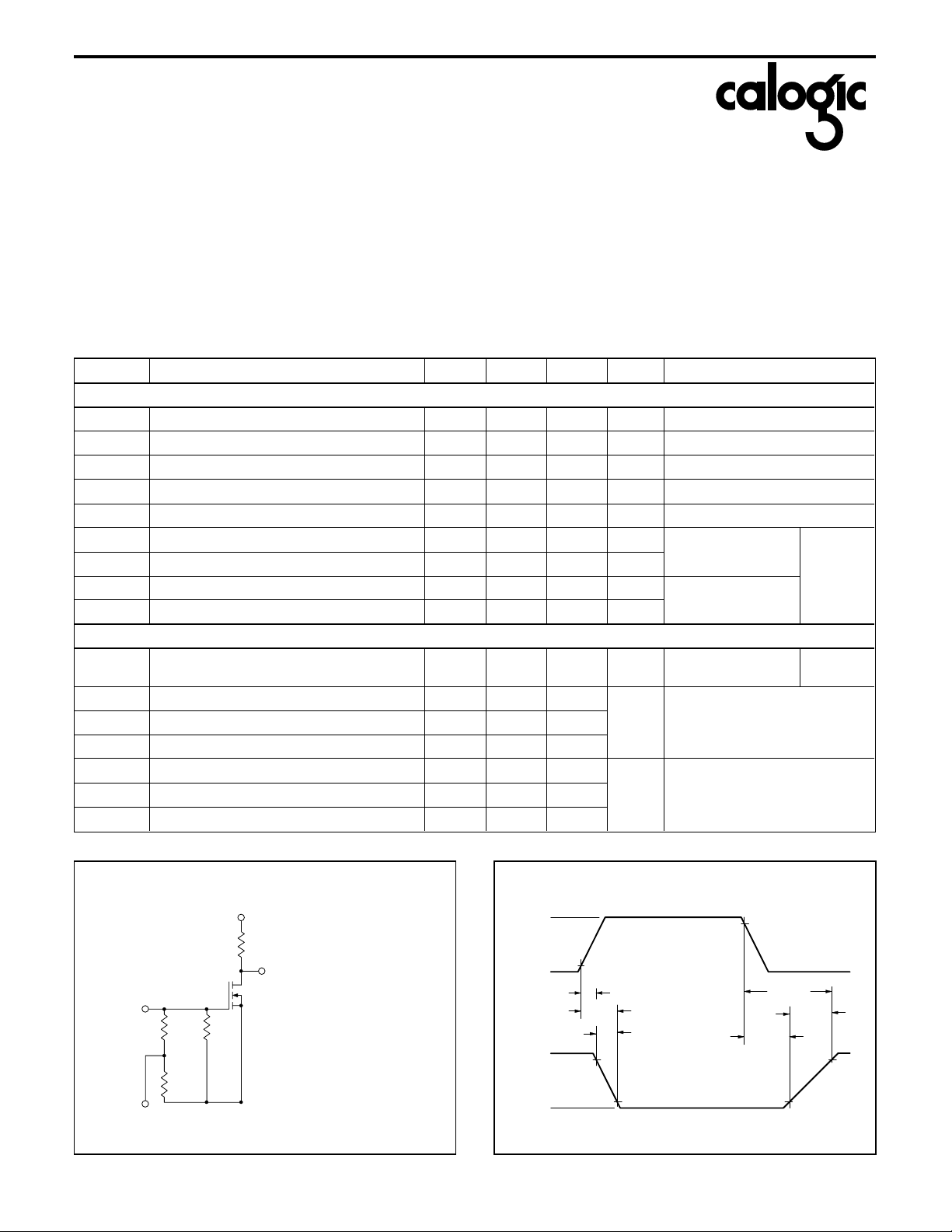
SWITCHING TIMES TEST CIRCUIT TEST WAVEF ORM S
V
V
G
510
51
OSCILLOSCOPE
DD
R
L
V
OUT
INPUT PULSE
<_
t 0.5 nSEC
R
Ω
G
Ω
r
PULSE WIDTH - 100 nSEC
SAMPLING OSCILLOSCOPE
t < 0.36 nSEC
r
R > 1M
Ω
in
C < 2.0 pF
in
V
G(on)
V
in
10%
0
t
d(on)
t
on
t
r
V
DD
90%
V
out
~
0V
~
10%
90%
t
d(off)
t
off
t
fall
90%
10%
 Loading...