

Calogic LLC SD403BD, SD403CY Datasheet
High Speed DMOS
N-Channel Switch
SD403
CORPORATION
FEATURES
Ultra High Speed Switching . . . . . . . . . . . . . . . . . tr < 1ns
••
Very Low Capacitance. . . . . . . . . . . . . . c
••
CMOS and TTL Compatible Input
••
Low ON Resistance . . . . . . . . . . . . . . . . . 40 ohms typical
••
APPLICATIONS
Switch Dri v e rs
••
Video Sw i tch es
••
Samples and Hold
••
Track and Hold
••
VHF/UHF Amplifie rs
••
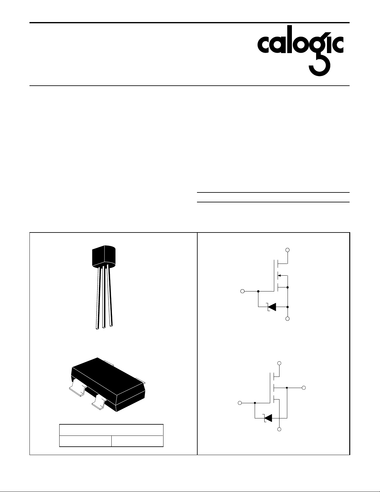
PIN CONFIGU R ATIO N
TO-92
0.4pf typica l
rss
DESCRIPTION
The Calogic SD403 is an N-Channel Enhancement-Mode
Lateral DMOS FET. This product has very low capacitance,
< 0.4pf typical ) allowing for high speed switching (tr 1ns).
(c
rss
The SD403 is a high gain device (19mmhos) and has good
performance values for sample and hold circuits, video
switches and switch driver s wh er e lowe r capacitance and high
speed switching are crit ical.
ORDERING INFORMATION
Part Package Temperature Range
o
SD403BD Plastic TO-92 -55 to +125
SD403CY SOT -143 Sur face Mount -55 to +125
XSD403 Sorted Chips in Carriers -55 to +125
SCHEMA TIC DIAGRAM
DRAIN
(2)
GATE
(3)
C
o
C
o
C
CD1-1
D
G
S
GATE (3)
BODY (4)
SOURCE (1)
PRODUCT MARKING
SD403CY SD403
DRAIN (2)
SOT-143
SOURCE
(1)
TO-92
DRAIN
(2)
BODY
(4)
GATE
(3)
SOURCE
(1)
SOT-143
CORPORATION
ABSOLUTE MAXIMUM RATINGS (TA = +25oC unless otherwise note d)
Drain-Source Voltage . . . . . . . . . . . . . . . . . . . . . . . . . . . +15V
Gate-Source Voltage. . . . . . . . . . . . . . . . . . . . . . . . . . . . -0.3V
+20V
Gate-Drain Voltage . . . . . . . . . . . . . . . . . . . . . . . . . . . . . -0.3V
+20V
Continuous Drain Curre nt . . . . . . . . . . . . . . . . . . . . . . . 50mA
Power Dissipation (at or below T
Linear Derating Factor. . . . . . . . . . . . . . . . . . . . . . 3.0mW/
Operating Junct ion and Storage
Temp eratur e Range . . . . . . . . . . . . . . . . -55
Source-Drain Voltage . . . . . . . . . . . . . . . . . . . . . . . . . . . -0.3V
SD403
= +25oC). . . . . . . . 300m W
A
o
C to +125oC
o
C
ELECTRICAL CHARACTERISTICS (T
= +25oC unless otherwise specified)
A
SYMBOL CHARACTERISTICS MIN TYP MAX UNIT TEST CONDITIONS
STATIC
Drain-Source Breakdown Voltage 15 25 V ID = 1.0µA, VGS =0
BV
DSS
I
D(OFF)
I
GSS
I
D(ON)
V
GS(th)
V
DS(ON)
r
DS(ON)
V
DS(ON)
r
DS(ON)
Drain-Source OFF Leakage Current 1.0 µAVDS = 15V, VGS = 0
Gate-Source Leakage Current 1.0 µAVGS = 20V, VDS = 0
Drain-Source ON Current 80 120 mA VDS = 10V, VGS = 10 V Pulse Test
Gate-Source Threshold Voltage 0.3 1.5 V ID = 1.0µΑ, VDS = V
Drain-Source ON Voltage 140 175 mV
Drain-Source ON Resistance 140 175 ohms
Drain-Source ON Voltage 40 60 mV
Drain-Source ON Resistance 40 60 ohms
= 1mA, VGS = 2.4V
I
D
= 1mA, VGS = 4.5V
I
D
GS
DYNAMIC
= 20 mA VDS = 10V,
I
gfs Common-Source Forward Transconductance 15 19 mS
c
iss
c
oss
c
rss
Common-Source Input Capacitance 4.5 6.0
Common-Source Output Capacitance 2.0 3.0
Common-Source Reverse Transfer Capacitance 0.4 0.6
td(on) Turn ON Delay Time 0.8 1.2
t
r
t
(OFF)
Rise Time 0.9 1.2
Turn OFF Time 1.4
D
f = 1KHz Pulse Test
V
= 10V, VGS = 0
pf
ns
DS
f = 1MHz
= 10V, RL = 680Ω
V
DD
V
= 10V, RG = 51Ω
G(ON)
C
= 1. 5pF
L
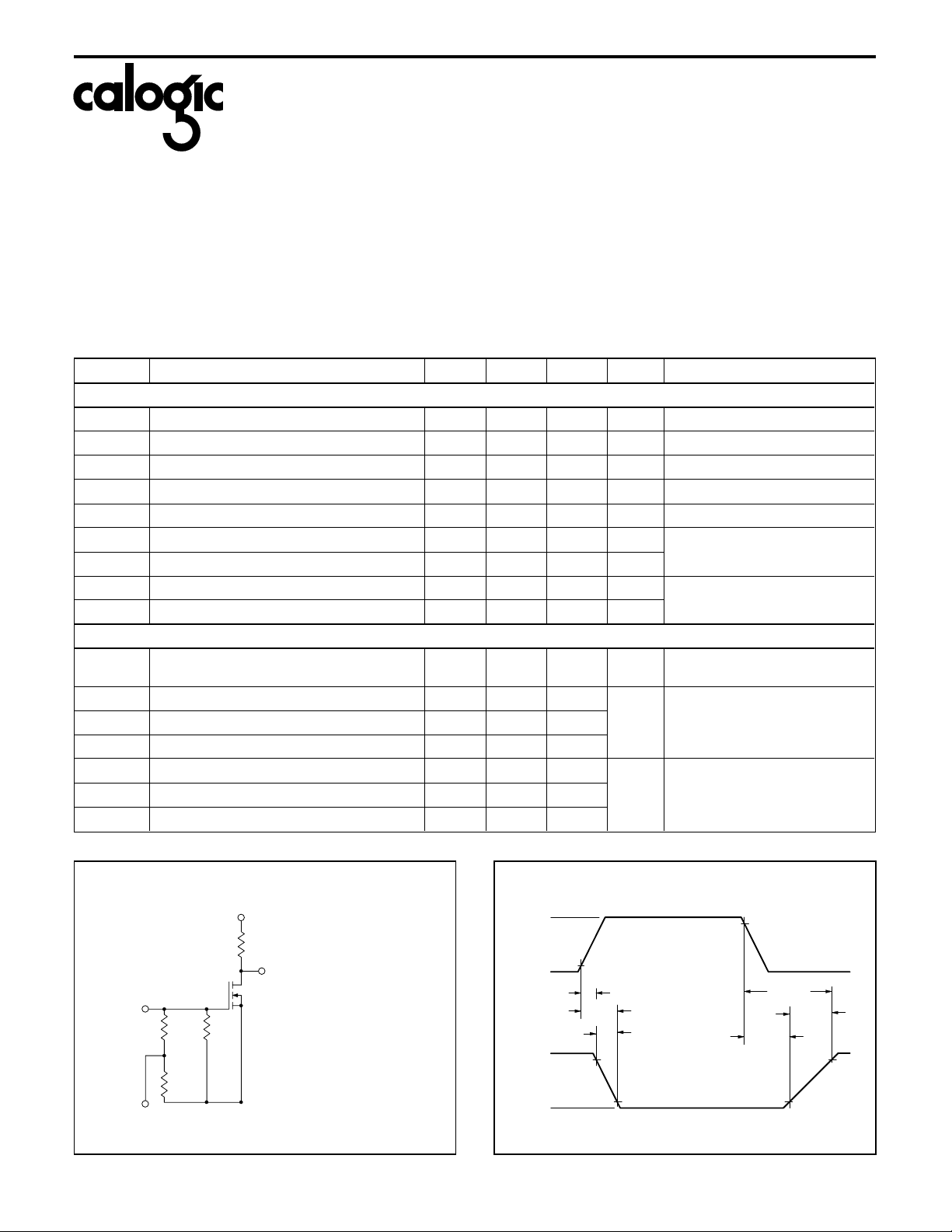
SWITCHING TIMES TEST CIRCUIT TEST WAVEF ORM S
V
V
G
510
51
OSCILLOSCOPE
DD
R
L
V
OUT
INPUT PULSE
<_
t 0.5 nSEC
R
Ω
G
Ω
r
PULSE WIDTH - 100 nSEC
SAMPLING OSCILLOSCOPE
t < 0.36 nSEC
r
R > 1M
Ω
in
C < 2.0 pF
in
V
G(on)
V
in
10%
0
t
d(on)
t
on
t
r
V
DD
90%
V
out
~
0V
~
10%
90%
t
d(off)
t
off
t
fall
90%
10%
 Loading...