

Calogic LLC SD200DC, SD201DC, SD202DC, SD203DC Datasheet
High-Speed Analog
N-Channel Enhancement-Mode
DMOS FETS
SD200 / SD201 / SD202 / SD203 / SSTSD201 / SSTSD203
FEATURES
••
High gain . . . . . . . . . . . . . . . . . . . . . 8.0 dB min @ 1 GHz
••
Low Noise. . . . . . . . . . . . . . . . . . . . . 5.0 dB max @ 1 GHz
(SD202, SD203, SSTSD203)
Low Inte rel ectrode Capacitances
APPLICATIONS
••
High Gain VHF/ UHF Am plif iers
••
Oscillators
••
Mixers
DESCRIPTION
The SD200 series is manufactured utilizing Calogic’s
proprietary DMOS design and processing techniques. The
device is designed to operate well through 1 GHz while
maintaining excellent frequency response, power gain, and
low noise. The DMOS structure is an inherently low
capacitance and very high speed design resulting in a device
that bridges JFETS and GaAs products in performance
characteristics.
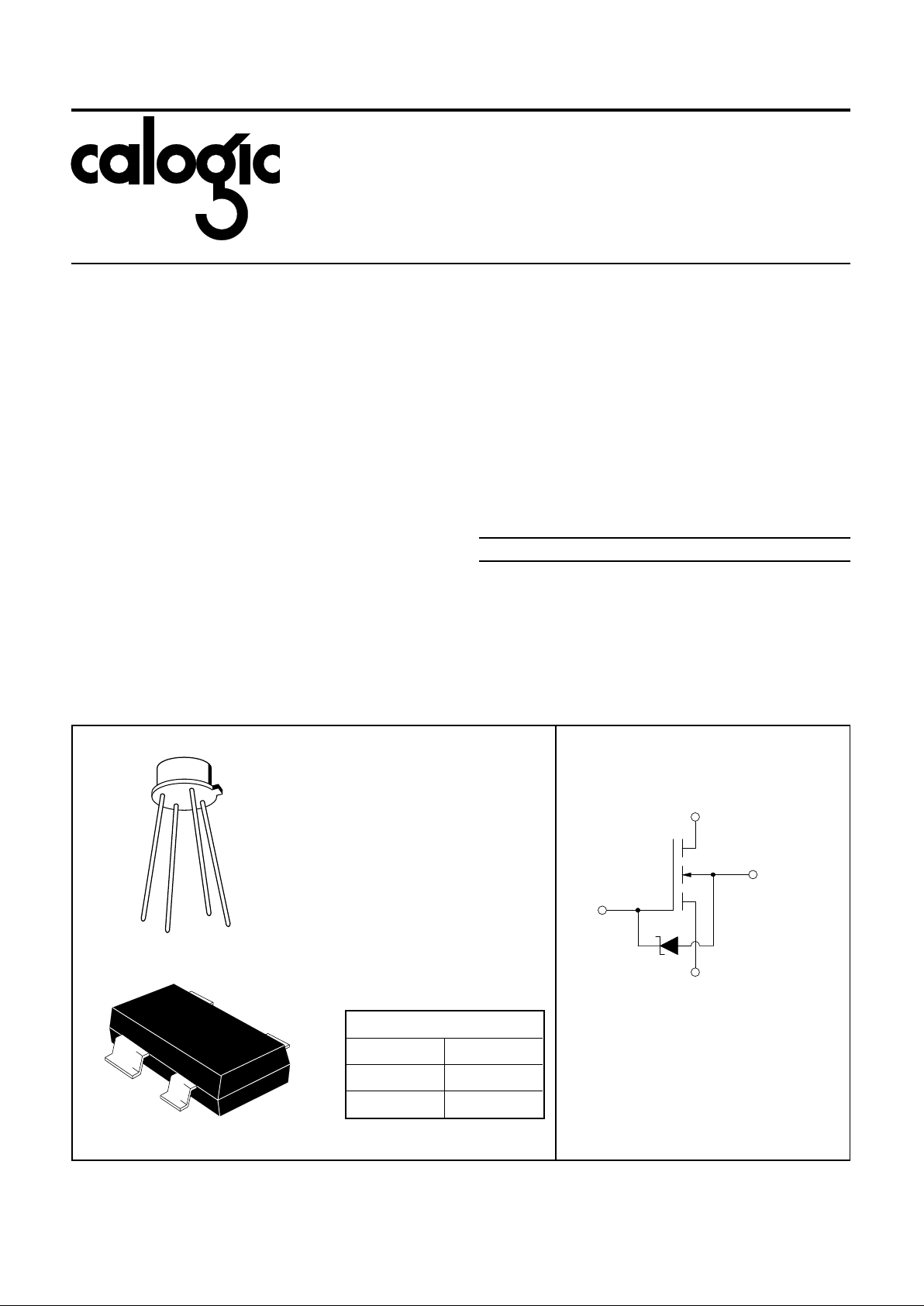
ORDERING INFORMATION
Part Package Temperature Range
SD200DC 4 Lead TO-52 Packa ge -55
o
C to +125oC
SD201DC 4 Lead TO-52 Packa ge -55
o
C to +125oC
SD202DC 4 Lead TO-52 Packa ge -55
o
C to +125oC
SD203DC 4 Lead TO-52 Packa ge -55
o
C to +125oC
SSTSD201 Surface Mount SOT-143 -55
o
C to +125oC
SSTSD203 Surface Mount SOT-143 -55
o
C to +125oC
XSD200 Sorted Chips in Carriers -55
o
C to +125oC
XSD201 Sorted Chips in Carriers -55
o
C to +125oC
XSD202 Sorted Chips in Carriers -55
o
C to +125oC
XSD203 Sorted Chips in Carriers -55
o
C to +125oC
CORPORATION
PIN CONFIGUR ATIO N SCHEMATIC DIAGRAM
(3)
GATE
(2)
DRAIN
(1)
SOURCE
BODY INTERNALLY CONNECTED TO CASE.
DIODE PROTECTION ON SD201/SD203 ONLY.
(4)
CASE, BODY
G
D
CASE, B
S
CD10-1 SD201, SD203, zener protected
CD10-2 SD202, SD204, non-zener
BODY (4)
SOURCE (1)
DRAIN (2)
GATE (3)
SOT-143
PART MARKINGS (SOT-143)
P/N MARKING
SSTSD201 201
SSTSD203 203
SD200 / SD201 / SD202 / SD203 / SSTSD201 / SSTSD203
CORPORATION
ABSOLUTE MAXIMUM RATING (TA = +25oC unless otherwise note d)
P ARAMETER SD200 SD201 SD202 SD203 UNIT
Breakdown
V olt ages
V
DS
+25 +25 +20 +20 V
V
DB
+25 +25 +20 +20 V
V
GS
±40 -0.3 ±40 -0.3 V
+20 +20 V
V
GB
±40 -0.3 ±40 -0.3 V
+20 +20 V
V
GD
±40 -0.3 ±40 -0.3 V
+20 +20 V
I
D
Continuous Drain Curren t . . . . . . . . . . . . . . . . . . 50 mA
P
T
Power Dissipation (at or below TC = +25oC) . . . . 1.8 W
Linear Derating Factor. . . . . . . . . . . . . . . . . 18 mW/
o
C
P
D
Power Dissipation (at or below TA = +25C). . . 360 mW
Linear Derating Facto r. . . . . . . . . . . . . . . . . 3.6 mW/
o
C
T
j
Operating Jun ctio n
Temperatu r e Range. . . . . . . . . . . . . . -55
o
C to + 125oC
T
s
Storage Temperature Range . . . . . . . . -65oC to +175oC
SYMBOL PARAMETER
200, 201 202 , 203
UNIT TEST CONDITIONS
MIN TYP MAX MIN TYP MAX
STATIC
BV
DS
Drain-Source Breakdown Voltage 25 30 20 25 V ID = 1.0µA, VGS = VBS = 0
BV
DB
Drain-Body Breakdown Voltage 25 20 V
I
D
= 1.0µA, VGB = 0
Source OPEN
I
D(OFF)
Drain-Source
OFF Current
1.0
µA
V
DS
= 25 V
V
GS
= VBS = 0
1.0 V
DS
= 20 V
I
GBS
Gate-Body
Leakage
Current
SD200 ±0.1
nA V
GV
= ±40 V
V
DB
= VSB = 0
SD202 ±0.1
SD201 1.0
µAV
GB
= 20 V
SD203 1.0
V
GS(th
) Gate Threshold Voltage 0.1 1.0 2.0 0.1 1.0 2.0 V VDS = VGS, ID = 1µA, VSB = 0
r
DS(ON)
Drain-Source ON Resistance 40 70 35 50 ohms VGS = 5 V, ID = 1 mA, VSB = 0
DYNAMIC
g
fs
Common-Source Forward
Transcondconductance
13 14 17 20 mS
I
D
= 20 mA, VDS = 15 V
f = 1 KHz, V
SB
= 0
c
iss
Common-Source Input Capacitance 2.4 3.0 3.0 3.6
pF
ID = 20 mA
V
DS
= 15 V
f = 1 MHz
V
SB
= 0
c
oss
Common-Source Output Capacitance 1.0 1.2 1.0 1.2
V
GS
= 0
c
rss
Common-Source
Reverse Transfer Capacitance
0.2 0.3 0.2 0.3
G
ps
Common-Source Power Gain 8.0 10 8.0 10
dB
V
DS
= 15 V
f = 1 GHz
ID = 20 mA
V
SB
= 0
NF Noise Figure 4.5 6.0 4.0 5.0
P
i
Intercept Point 29 29 dBm ∆f = 2 MHz
ELECTRICAL CHARACTERISTICS (TA = +25oC unless otherwise note d)
 Loading...