

Calogic LLC LP2951CS-3, LP2951CP-5, LP2951CP-3.3, LP2951CS-5, LP2951CS-3.3 Datasheet
...
100mA Low Dropout
Voltage Regulators
LP2950 / LP2951
FEATURES
••
5V, 3.3V, and 3.0V Vers io ns at 100mA Output
••
Ver y Low Q ui e s cent Current
••
Low Dropout Voltage
••
Extremely Tig h t Load and Line Regul ati on
••
Ver y Low Tempe ratur e Coef fi ci ent
••
Current and Thermal Limiting
••
Needs Only 1µF for Stabi lit y
LP2951 Versions Only
••
Error Flag Warns of Output Dropout
••
Logic-Controlled Electronic Shutdown
••
Outpu t Progr am ma bl e from 1. 24 to 2 9V
APPLICATIONS
••
Battery Pow er ed Syst em s
••
Cordless Telephones
••
Radio Control Systems
••
Portable / Palm T op / Noteboo k Comput ers
••
Portable Consumer Equipment
••
Portable I nst ru me nt atio n
••
Avionics
••
SMPS Post-Regula tor
••
V ol tage Ref er en c e
••
Automot i ve El ect r oni cs
PRODUCT DESCRIPTION
The Calogic LP2950 and LP2951 are low power voltage
regulators. These devices are an excellent choice for use in
battery-powered applications such as cordless telephones,
radio control systems, and portable computers. The LP2950
and LP2951 features very low quiescent current and very low
dropout volt age (Typ. 50mV at light load and 380mV at 100mA).
This includes a tight initial tolerance of 0.5% typ., extremely
good load and line regula tion 0.05% typ. and very low output
temperature coefficient, making the LP2950/LP2951 useful
as a low-power voltage reference.
The error flag output feature is used as power-on reset for
warning of a low output voltage, due to falling voltage input of
batteries. Another feature is the logic-compatible shutdown
input which enables the regulator to be switched on and off.
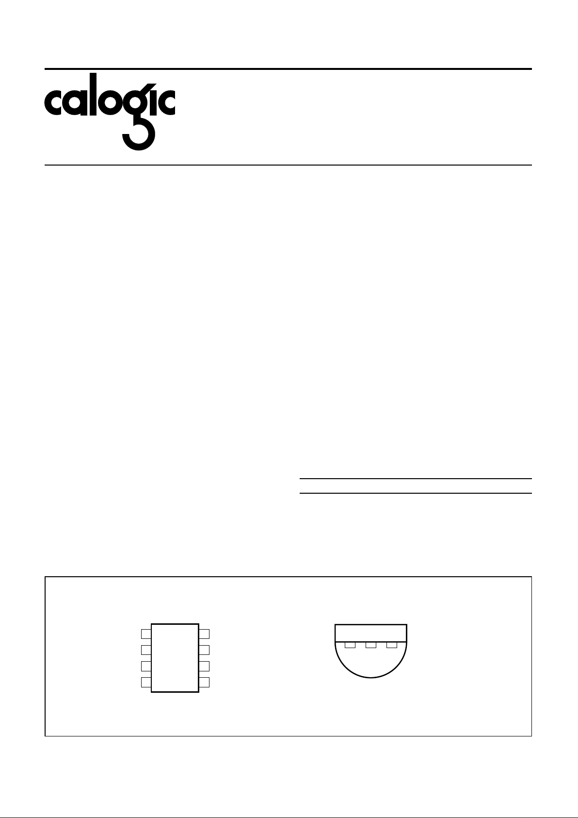
The LP2950 is offered in a 3-pin TO-92 package compatible
with other 5V , 3.0V, 3.3V regulators. The LP2951 is also av ailabl e
in 8-pin plastic and SO- 8.
The regulator output voltage may be pin-strapped for 5V, 3V
or 3.3 volts or programmed from 1.24 volt to 29 volts with an
external pair of resistors. Use of AS’s design, processing and
testing techniques make our LP2950 and LP2951 superior
over similar product s.
ORDERING INFORMATION
P ART PACKAGE TEMPERATURE RANG E
LP2950ACN-X TO-92 (3-Pin) IND.
LP2950CN-X TO-92 (3-Pin) IND.
LP2951ACP-X Plastic DIP (8-Pin) IND.
LP2951CP-X Plastic DIP (8-Pin) IND.
LP2951ACS-X Plastic SOIC (8-Pin) IND.
LP2951CS-X Plastic SOIC (8-Pin) IND.
X = 3.0V, 3.3V or 5.0V
CORPORATION
PIN CONNECTIONS
1D-20
123
1. OUTPUT
2. GROUND
3. INPUT
TO-92
BOTTOM VIEW
GROUND
1
2
3
8
7
6
4 5 ERROR
LP2951
1D-19
8-PIN SURFACE MOUNT
5V OR 3.3V TAP
FEEDBACK
INPUT
SHUTDOWN
SENSE
OUTPUT
TOP VIEW
CALOGIC CORPORATION, 237 Whitney Place, Fremont, California 9453 9, Telephone: 510 -656- 2900, FAX: 510-651-3025
ABSOLUTE MAXIMUM RATINGS
Power Dissipation . . . . . . . . . . . . . . . . . . . . . Internally Limited
Lead Temp. (Soldering, 5 Seconds) . . . . . . . . . . . . . . . 260
o
C
Storage Tem per atur e Ra nge. . . . . . . . . . . . . . . -65 to +150
o
C
Operating Junct ion Te mper at ure Ra nge
LP2951. . . . . . . . . . . . . . . . . . . . . . . . . . . . . . -55 to +150
o
C
LP2950AC/LP2950C
LP2951AC/LP2951C. . . . . . . . . . . . . . . . . . . -40 to +125
o
C
Input Supply Vo ltag e . . . . . . . . . . . . . . . . . . . . . . -0.3 to +30V
Feedback Input Voltage. . . . . . . . . . . . . . . . . . . . -1.5 to +30V
Shutdown Input Voltage. . . . . . . . . . . . . . . . . . . . -0.3 to +30V
Error Comparator Output. . . . . . . . . . . . . . . . . . . -0.3 to +30V
ESD Rating . . . . . . . . . . . . . . . . . . . . . . . . . . . . . . . . 2KV Min
LP2950 / LP2951
CORPORATION
CALOGIC CORPORATION, 237 Whitney Place, Fremont, California 9453 9, Telephone: 510 -656- 2900, FAX: 510-651-3025
ELECTRICAL CHARACTERISTICS: V
S
= 15V, TA = 25oC, unless otherwise specified .
PARAMETER
LP2951 LP2950AC / LP2951AC LP2950C / LP2951C
UNITS
CONDITIONS
(Note 2)
MIN TYP MAX MIN TYP MAX MIN TYP MAX
3V VERSIONS
Output Voltage
2.985
2.964
3.0 3.015
3.036
2.985
2.970
2.964
3.0
3.0
3.0
3.015
3.030
3.036
2.970
2.955
2.940
3.0
3.0
3.0
3.030
3.045
3.060
V
V
V
TJ = 25oC
-25
o
C ≤ TJ ≤ 85oC
Full Operating T emperature
Output Voltage 2.955 3.0 3.045 2.958 3.0 3.042 2.928 3.0 3.072 V
100µA ≤ I
L
≤ 100mA
T
J
≤T
JMAX
3.3V VERSIONS
Output Voltage
3.284
3.260
3.3 3.317
3.340
3.284
3.267
3.260
3.3
3.3
3.3
3.317
3.333
3.340
3.267
3.251
3.234
3.3
3.3
3.3
3.333
3.350
3.366
V
V
V
T
J
= 25oC
-25
o
C ≤ TJ ≤ 85oC
Full Operating T emperature
Output Voltage 3.251 3.3 3.350 3.254 3.3 3.346 3.221 3.3 3.379 V
100µA ≤ I
L
≤ 100m A
T
J
≤T
JMAX
5V VERSIONS
Output Voltage
4.975
4.94
5.0 5.025
5.06
4.975
4.95
4.94
5.0
5.0
5.0
5.025
5.050
5.06
4.95
4.925
4.90
5.0
5.0
5.0
5.05
5.075
5.10
V
V
V
T
J
= 25oC
-25
o
C ≤ TJ ≤ 85oC
Full Operating T emperature
Output Voltage 4.925 5.0 5.075 4.93 5.0 5.07 4.88 5.0 5.12 V
100µA ≤ I
L
≤ 100m A
T
J
≤ T
JMAX
ALL VOLTAGE OPTIONS
Output Voltage
T emperature Coefficient
20 120 20 50 ppm/
o
C (Note 1)
Line Regulation (Note 3) 0.03 0.1 0.03 0.1 0.04 0.2 % 6V ≤ V
IN
≤ 30V (Note 4)
Load Regulation (Note 3) 0.04 0.1 0.04 0.1 0.1 0.2 % 100µA ≤ I
L
≤ 100m A
Dropout Voltage
(Note 5)
50
38080450
50
38080450
50
38080450mVmV
I
L
= 100µA
I
L
= 100m A
Ground Current
1508170
12
1508170
12
1508170
12
µAmAI
L
= 100µA
I
L
= 100m A
Current Limit 130 200 130 200 130 200 mA V
OUT
= 0
Thermal Regulation 0.05 0.2 0.05 0.2 0.05 0.2 %/W
Output Noise,
10Hz to 100KHz
430
160
100
430
160
100
430
160
100
µVrms
µVrms
µVrms
C
L
= 1µF
C
L
= 200µF
C
L
= 13.3µF
(Bypass = 0.01µF pins 7 to 1 (LP2951))
8-PIN VERSIONS ONLY LP2951 LP2951AC LP2951C
Reference Voltage 1.22 1.235 1.25 1.22 1.235 1.25 1.21 1.235 1.26 V
Reference Voltage 1.19 1.27 1.19 1.27 1.185 1.285 V Over Temperature (Note 6)
Feedback Pin Bias Current 40 60 40 60 40 60 nA
Reference Voltage
T emperature Coefficient
20 20 50 ppm/
o
C (Note 7)
Feedback Pin Bias Current
T emperature Coefficient
0.1 0.1 0.1 nA/
o
C
LP2950 / LP2951
CORPORATION
BLOCK DIAGRAM
ERROR DETECTION
COMPARATOR
1D-21
1µF
REFERENCE
1.23V
UNREGULATED DC
ERROR
AMPLIFIER
60mV
+
+
TO CMOS OR
TTL
330kΩ
FROM
CMOS
OR TTL
+
+
5V @ 100mA
MAX
60kΩ
LP2950 AND LP2951 BLOCK DIAGRAM
180kΩ
817
SENSE
6
2
4
5
5V TAP
ERROR
GROUND
INPUT OUTPUTFEEDBACK
SHUTDOWN
3
–
+
–
+
CALOGIC CORPORATION, 237 Whitney Place, Fremont, California 9453 9, Telephone: 510 -656- 2900, FAX: 510-651-3025
ELECTRICAL CHARACTERISTIC S (continued)
PARAMETER
LP2951 LP2950AC / LP2951AC LP2950C / LP2951C
UNITS
CONDITIONS
(Note 2)
MIN TYP MAX MIN TYP MAX MIN TYP MAX
ERROR COMPARATOR
Output Leakage Current 0.01 1 0.01 1 0.01 1 µAV
OH
= 30V
Output Low Voltage 150 250 150 250 150 250 mV V
IN
= 4.5V, IOL = 400µA
Upper Threshold Voltage 40 60 40 60 40 60 mV (Note 7)
Lower Threshold Voltage 75 95 75 95 75 95 mV (Note 7)
Hysteresis 15 15 15 mV (Note 7)
SHUTDOWN INPUT
Inp ut Logic Voltage
2
1.3 0.6
2
1.3 0.7
2
1.3 0.7 V
V
Low (Regulato r ON)
High (Regulator OFF)
Shutdown Pin
Input Current
30
67550800
30
67550800
30
67550800
µAµAV
S
= 2.4V
V
S
= 30V
Regulator Output Current
in Shutdown
310 310 310µA (Note 9)
Note 1: Output or reference voltage temperature coefficients defined as the worst case voltage change divided by the total temperature range.
Note 2: Unless otherwise specified all limits guaranteed for T
J
= 25oC, VIN = 6V, IL=100µA and CL = 1µF. Additional conditions for the 8-pin
versions are feedback tied to 5V tap and output tied to output Sense (V
OUT
= 5V) and V
SHUTDOWN
≤ 0.8V.
Note 3: Regulation is measured at constant junction temperature, using pulse testing with a low duty cycle. Changes in output voltage due to
heating effects are covered under the specification for thermal regulation.
Note 4: Line regulation for the LP2951 is tested at 150
o
C for IL = 1mA. For IL = 100µA and TJ = 125oC, line regulatio n is guara nte ed by desig n to
0.2%. See typical performance characteristics for line regulation versus temperature and load current.
Note 5: Dropout voltage is defined as the input to output differential at which the output voltage drops 100mV below its nominal value measured
at 1V differential at very low values of programmed output voltage, the minimum input supply voltage of 2V (2.3V over temperature) must be
taken input account.
Note 6: V
REF
≤ V
OUT
≤ (VIN - 1V), 2.3 ≤ VIN ≤ 30V, 100µA ≤ IL ≤ 100mA, TJ ≤ T
JMAX
.
Note 7: Comparator thresholds are expressed in terms of a voltage differential at the feedback terminal below the nominal reference voltage
measured at 6V input. To express these thre sh old s in terms of output vo lta ge chan ge , mu ltip l y by the erro r amp lifi er g ai n = V
OUT/VREF
=
(R1+R2)/R2. For example, at a programmed output voltage of 5V, the error output is guaranteed to go low when the output drops by 95 mV x
5V/1.235 = 384mV. Thresho lds remain constant as a percent of V
OUT
as V
OUT
is varied, with the dropout warning occurring at typically 5% below
nominal, 7.5% guaranteed.
Note 8: V
SHUTDOWN
≥ 2V, VIN ≤ 30V, V
OUT
= 0, Feedback pin tied to 5V Tap.
Note 9: All typical values are not guaranteed.
 Loading...