

Calogic LLC J309, J310, J308 Datasheet
CORPORATION
N-Channel JFET
High Frequency Amplifier
J308 – J310 / SST308 – SST310
FEATURES
Industry Stand ard Pa rt in Low Cost Plastic Package
••
High Powe r Gain
••
Low Noise
••
Dynamic Range G r eat er Than 10 0dB
••
Easily Matched to 75Ω Input
••
APPLICATIONS
VHF/UHF Amplifie rs
••
Oscillators
••
Mixers
••
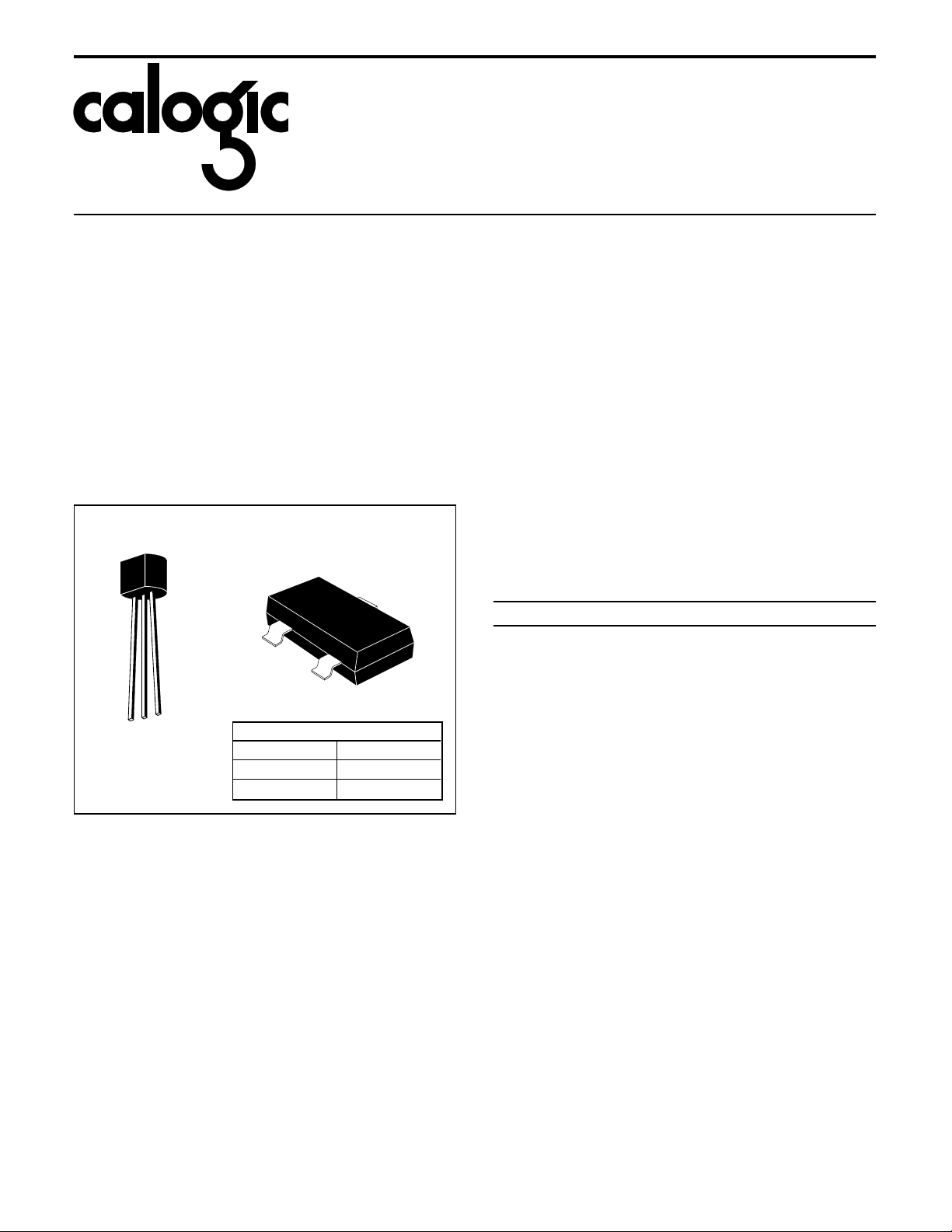
PIN CONFIGU R ATION
SOT-23
G
TO-92
D
S
G
S
D
5021
PRODUCT MARKING (SOT-23)
SST308 Z08
SST309 Z09
SST310 Z10
ABSOLUTE MAXIMUM RATINGS
= 25oC unless otherwise specified)
(T
A
Drain-Gate Voltage . . . . . . . . . . . . . . . . . . . . . . . . . . . . . -25V
Drain-Source Voltage. . . . . . . . . . . . . . . . . . . . . . . . . . . . -25V
Continuous Forwar d Gate Cur rent . . . . . . . . . . . . . . . . -10mA
Storage Temperatur e Ra nge. . . . . . . . . . . . . -5 5
Operating Temperatur e Ra nge . . . . . . . . . . . -55
Lead Temperature (Soldering, 10se c). . . . . . . . . . . . . +300
Power Dissipation . . . . . . . . . . . . . . . . . . . . . . . . . . . . 360mW
Derate above 25
NOTE: Stresses above those listed under "Absolute Maxi mum
Ratings" may cause permanent damage to the device. These are
stress ratings only and functional operation of the device at these or
any other conditions above those indicated in the operational sections
of the specifications is not implied. Exposure to absolute maximum
rating conditions for extended periods may affect device reliability.
ORDERING INFORMATION
Part Package Temperature Range
J308-310 Plastic TO- 92 -55
SST308-310 Plastic SOT - 23 -55
For Sorted Chips in Carr iers see U308 serie s.
o
C . . . . . . . . . . . . . . . . . . . . . . 3.27 mW/oC
o
C to +150oC
o
C to +135oC
o
C to +135oC
o
C to +135oC
o
C
J308 – J310 / SST308 – SST310
ELECTRICAL CHARACTERISTIC S (TA = 25oC unless otherwise sp ecif ied)
CORPORATION
SYMBOL PARAMETER
BV
I
GSS
V
GS(off)
I
DSS
V
GS(f)
g
fs
g
os
g
fg
g
og
Gate-Source Breakdown
GSS
Voltage
Gate Reverse Current
Gate-Source
Cutoff Voltage
Saturation Drain Current
(Note 1)
Gate-Source
Forward Voltage
Common-Source Forward
Transconductance
Common-Source Output
Conductance
Common-Gate Forward
Transconductance
Common Gate Output
Conductance
8,000 17,000 10,000 17,000 8,000 17,000
308 309 310
MIN TYP MAX MIN TYP MAX MIN TYP MAX
-25 -25 -25 V I
-1.0 -1.0 -1.0 nA V
-1.0 -1.0 -1.0 µAV
-1.0 -6.5 -1.0 -4.0 -2.0 -6.5 V VDS = 10V, I
12 60 12 30 24 60 mA V
1.0 1.0 1.0 V V
250 250 250
13,000 13,000 12,000
150 150 150
ELECTRICAL CHARACTERISTIC S (Continued) (TA = 25oC unless otherwise specified)
SYMBOL PARAMETER
C
gd
C
gs
e
n
Gate-Drain Capacitance 1.8 2.5 1.8 2.5 1.8 2.5
Gate-Source Capacitance 4.3 5.0 4.3 5.0 4.3 5.0
Equivalent Short-Circuit
Input Noise Voltage
308 309 310
MIN TYP MAX MIN TYP MAX MIN TYP MAX
10 10 10
√
Hzü⁄
ç4«ónVçXIÇÀçXäBÇÇG‘•çQXóHzâÏé
UNITS TEST CONDITIONS
= -1µA, VDS = 0
G
= -15V,
GS
= 0 TA = 125
DS
= 1nA
D
= 10V, VGS = 0
DS
= 0, IG = 1mA
DS
= 10V
V
DS
I
µS
= 10mA
D
(Note 2)
f = 1kHz
UNITS TEST CONDITIONS
V
pF
nV
= 10V ,
DS
V
= -10
GS
VDS = 10V ,
I
= 10mA
D
f = 1MHz
(Note 2)
f = 100Hz
(Note 2)
o
Re
Re
Re
Re
G
pg
(Vfs)
(Vfg)
(Vis)
(Vos)
Common-Source Forward
Transconductance
Common-Gate Input
Conductance
Common-Source Input
Conductance
Common-Source Output
Conductance
Common-Gate Power Gain
at Noise Match
12 12 12
14 14 14
0.4 0.4 0.4
0.15 0.15 0.15
16 16 16
NF Noise Figure 1.5 1 .5 1.5
G
pg
Common-Gate Power Gain
at Noise Match
11 11 11
NF Noise Figure 2.7 2 .7 2.7
NOTES: 1. Pulse test PW 300µs, duty cycle ≤3%.
2. For design reference only, not 100% tested.
µS
dB
V
= 10V ,
DS
I
= 10mA
D
(Note 2)
f = 105MHz
f = 450MHz
 Loading...