

Calogic LLC CWB211CY, CWB211CP Datasheet
100MHz CMOS/DMOS
Wideband Analog Switch
CWB211
CORPORATION
FEATURES
Ultra Low Leakage. . . . . . . . . . . . . ID(
••
Low Capaci t a nce . . . . . . . . . . . . . . . . . . . cd 0.3pf typical
••
Low ON Resistance . . . . . . . . . . . . . . . . . . . . 40 Ω typical
••
TTL Co m patible
••
200pA typical
OFF)
APPLICA TI ONS
Glitch-Free Analog Switches
••
RF & Video Sw itc h es
••
Sample-an d-Hol d Sw itch es
••
Communication Systems
••
Disk Driv es
••
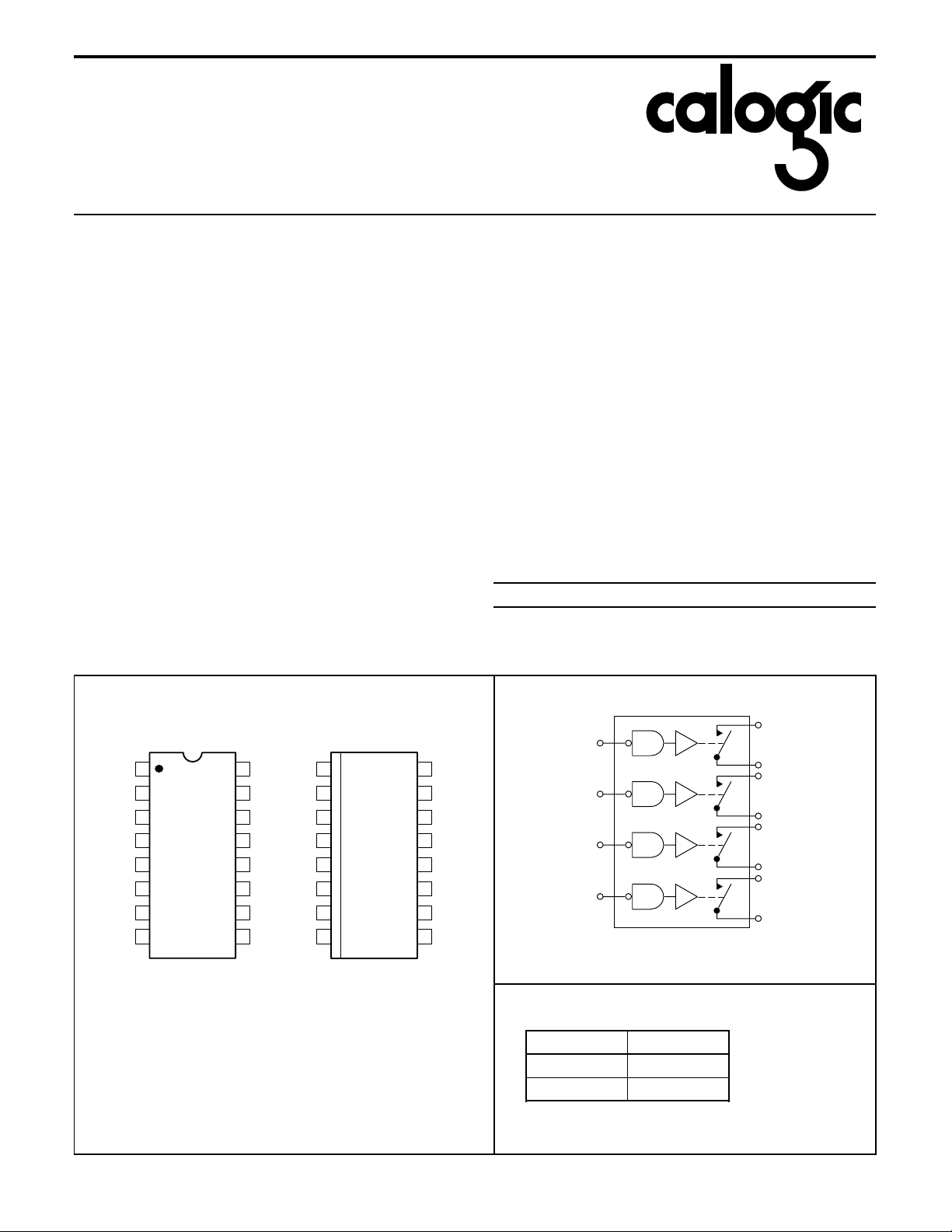
PIN CONFIGU R ATI ON
16 PIN DIP SO-16
IN1
GND
IN4
1
2
D1
3
S1
4
V-
5
6
S4
7
D4
8
TOP VIEW
CWB211CP
IN2
16
D2
15
S2
14
V+
13
N/C
12
S3
11
D3
10
IN3
9
IN1
GND
IN4
1
2
D1
3
S1
4
V-
5
6
S4
7
D4
8
TOP VIEW
CWB211CY
CWB
NOTE: All devices contain d iodes to protect inp uts against
damage due to high static voltages or electric fields;
however, it is advised that precautions be taken not to
exceed the maximum recommended input voltages. All
unused inputs must be connected to an appropriate logic
level (V
or GND).
DD
DESCRIPTION
The Calogic CWB211 offers designers high performance at a low
cost. The CWB21 1 is an excellent choice where capacitance an d
switching times are crucial. The device out performs industry
standard DG211 types offe ring mu ch f ast er sw it chi ng speeds, low
R
and lower capacitance while maintaining high OFF
DS (ON)
isola ti on and good ban dwidt h. The Cal ogic CWB 211 is configured
to be a pin for pin replacement of existing analog switches
and at the same time upgrading high frequency perfo rma nce.
Manufactured on the Calogic proprietary low voltage CMOS
combined with high speed DMOS FETs, the device is TTL
compatible utilizing an on-chip reference to provide constant
logic switching over a wide range of supply voltages and
temperatur e without a separ at e power sup ply.
ORDERING INFORMATION
Part Package Temperature Range
o
CWB211CP Plastic 16-Pin Dip 0 to +85
CWB21 1CY SO-16 Plastic 0 to +85
XCWB211 Sorted Chips in Carrier s 0 to +85
C
o
C
o
C
FUNCTIONAL BLOCK DIAGRAM
S
IN
1
16
IN2
15
D2
14
S2
13
V+
12
N/C
11
S3
10
D3
9
IN3
IN
2
IN
3
IN
4
Four SPST Switches per Package.
Switches shown in Logic '1' Input Position.
1
D
1
S
2
D
2
S
3
D
3
S
4
D
4
LOGIC TABLE
Logic Switch
0ON
1 OFF
Logic ’0’ ≤ 0.8V
Logic ’1’ ≥ 2.42V
CORPORATION
CWB211
ABSOLUTE MAXIMUM RATINGS
V- Negative Supply Voltage . . . . . . . . . . . . . . . . . . . . -20V
V+ Positive Supply V olt age. . . . . . . . . . . . . . . . . . . . . +20V
Control Input Vo ltag e Range . . . . . . . . . . . . . . V+ +0.3V
V
IN
V- -0.3V
Continuous Current, any Pin excep t S or D. . . . . . 20mA
I
L
I
Continuou s Curre nt, S or D . . . . . . . . . . . . . . . . . . 30mA
S
Peak Pulsed Current, S or D, 80µsec, 1%,
I
S
RECOMMENDED OPERAT ING CONDITION S
V- Negative Supply Voltage . . . . . . . . . . . . . . . -8.0 to -15V
V+ Positive Supply V olt age. . . . . . . . . . . . . . . +8.0 to +15V
Control Input Vo ltage Range . . . . . . . . . . . . . . 0 to +5V
V
IN
Operating Temperature . . . . . . . . . . . . . . . . 0 to +85oC
T
OP
Duty Cycle . . . . . . . . . . . . . . . . . . . . . . . . . . . . . . . 90mA
Junction Tempe ra ture Range. . . . . . . . . . -55 to +125oC
T
J
Storage Temper atur e Range. . . . . . . . . . -55 to +125oC
T
S
P
Power Dissipation . . . . . . . . . . . . . . . . . . . . . . . 500mW
D
0.8
= +25oC)
A
Ω
V
µA
nA
mA
nsec
dB
pF
= -10V
V
S
V
V
= +2.0V
S
= +10V
V
S
V
= +2.4V
IN
= +15V
V
IN
V
= +10V, VS = -10V
D
= +10V, VD = -10V
V
S
= 0 or +2.4V
V
IN
= 0
IN
See Switching Times Test Circuit
f = 10MHz, R
V
= VS = 0
D
= 50Ω
L
f = 1MHz
ELECTRICAL CHARACTERISTICS (V- = -15V, V+ = +15V unle ss otherwise n ot ed, T
SYMBOL PARAMETER MIN TYP MAX UNITS TEST CONDITIONS
STATIC
V
ANALOG
r
DS(ON)
V
IH
V
IL
I
IN
I
D(OFF)
I
S(OFF)
I- Negative Supply Quiescent Current
I+ Positive Supply Quiescent Current
DYNAMIC
t
ON
t
OFF
O
IRR
C
CRR
C
d
C
s
Analog Signal Range
Channel ON Resistance
High Level Input Voltage
Low Level Input Voltage
Logic Input Leakage Current
Switch OFF Leakage Current
Switch Turn-ON Time
Switch Turn-OFF Time
OFF Isolation Rejection Ratio
Cross Coupling Rejection Ratio
Drain-Node Capacitance
Source-Node Cap acita nce
-10 +10 V
40 80
45 80
100 160
2.4
0.01 0.1
0.02 0.1
0.2 5.0
0.4 5.0
-0.3 -1.0
0.6 2.0
400 600
70 300
60 66
80
0.3
3.0
V
=
IN
+2.4V
VIN =
+2.4V
ELECTRICAL CHARACTERISTICS (V- = -15V, V+ = +15V unless other wise no ted)
LIMITS A T TEMPERATURE EXTREMES
SYMBOL PARAMETER
STATIC
V
ANALOG
r
DS(ON)
I
IN
I
D(OFF)
I
S(OFF)
Analog Signal Range
Switch ON Resistance
Logic Input
Leakage Current
Switch OFF
Leakage Current
I- Negative Supply Quiescent Current
I+ Positive Supply Quiescent Current
MAXIMUM @ T
+85
±10 V
120
120
240
1.0
2.0
100
100
-1.0
2.0
=
A
o
C
UNITS TEST CONDITIONS
Ω
µA
nA
mA
= -10V
V
S
V
= +2.0V
S
= +10V
V
S
= +2.4V
V
IN
= +1 5V
V
IN
= +10V, VS = -10V
V
D
= +10V, VD = -10V
V
S
= 0 or +2.4V
V
IN
V
IN
V
IN
= 0
= +2.4V
 Loading...