

Calogic LLC CWB201CY, CWB201CP Datasheet
CORPORATION
100MHz CMOS/DMOS
Wideband Quad Analog Switch
CWB201
FEATURES
Wide Ban dw idt h Sw itch e s . . . . . . . . 0.9 x DC @ 100MHz
••
High OFF Isola tio n. . . . . . . . . . . . . . . . . 66 dB @ 100MHz
••
Low Channel-to-Channel Crosstalk. . . -80 dB @ 10MHz
••
TTL Co m patible
••
Low ON Resistance
••
High Spee d
••
Low Ca paciatance
••
APPLICATIONS
Glitch-Free Analog Switches
••
RF & Video Sw itc h es
••
Tr ac k -a nd - Ho l d Sw i tc he s
••
Sample-an d-Hol d Sw itch es
••
High Speed Data Routi ng
••
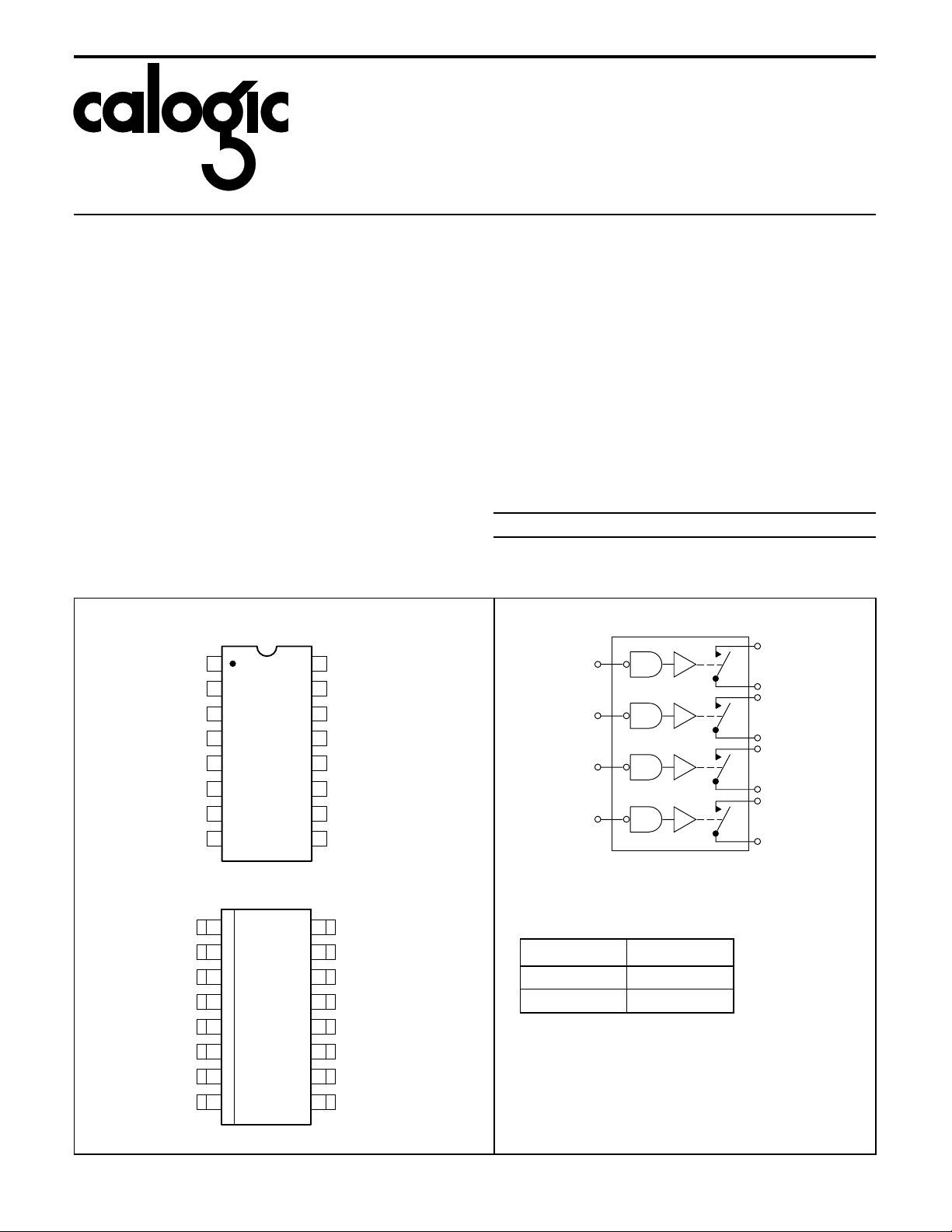
PIN CONFIGU R ATIO N
CWB201CP
IN1
D1
S1
GND
S4
D4
IN4
1
2
3
4
V-
5
6
7
8
IN2
16
D2
15
S2
14
V+
13
N/C
12
S3
11
D3
10
IN3
9
DESCRIPTION
Designed for RF and Video Switching the CWB201 is
manufactured using Calogic’s high speed CMOS combined
with DMOS transistors in a monolithic design resulting in
superior performance characteristics. This quad SPST switch
array has extensive applications where high frequency video,
audio or digi tal signals are switched or routed. The CWB201
is TTL compatible which is of great benefit to to designs that
require constant logic switching over a wide range of supply
voltages and tempe ratu re withou t a separ ate powe r supply.
ORDERING INFORMATION
Part Package Temperature Range
o
CWB201CP Plastic 16-Pin Dip 0 to +85
CWB201CY Plastic SO-16 Surface Mount 0 to +85
XCWB201 Sorted Chips in Carriers 0 to +85
C
o
C
o
C
FUNCTIONAL BLOCK DIAGRAM
S
IN
1
IN
2
IN
3
IN
4
1
D
1
S
2
D
2
S
3
D
3
S
4
D
4
CWB
IN1
D1
S1
GND
S4
D4
IN4
TOP VIEW
CWB201CY
1
2
3
4
V-
5
6
7
8
TOP VIEW
16
IN2
15
D2
14
S2
13
V+
12
N/C
11
S3
10
D3
9
IN3
LOGIC TABLE
NOTE: All devices conta in diodes t o protect inputs agai nst
damage due to high static voltages or electric fields;
however, it is advised that precautions be taken not to
exceed the maximum recommended input voltages. All
unused inputs must be connected to an appropriate logic
level (V
Four SPST Switches per Package.
Switches shown in Logic '1' Input Position.
Logic Switch
0ON
1 OFF
or GND).
DD
Logic ’0’ ≤ 0.8V
Logic ’1’ ≥ 2.42V
CWB201
CORPORATION
ABSOLUTE MAXIMUM RATINGS
V- Negative Supply Voltage . . . . . . . . . . . . . . . . . . . . -20V
V+ Positive Supply Volt age. . . . . . . . . . . . . . . . . . . . . +20V
Control Input Vo ltag e Range . . . . . . . . . . . . . . V+ +0.3V
V
IN
V- -0.3V
Continuous Current, any Pin excep t S or D. . . . . . 20mA
I
L
I
Continuou s Curre nt, S or D . . . . . . . . . . . . . . . . . . 30mA
S
Peak Pulsed Current, S or D, 80µsec, 1%,
I
S
RECOMMENDED OPERAT ING CONDITION S
V- Negative Supply Voltage . . . . . . . . . . . . . . . -8.0 to -15V
V+ Positive Supply V olt age. . . . . . . . . . . . . . . +8.0 to +15V
Control Input Vo ltage Range . . . . . . . . . . . . . . 0 to +5V
V
IN
Operating Temperatur e . . . . . . . . . . . . . . . . . . 0 to 85oC
T
OP
Duty Cycle . . . . . . . . . . . . . . . . . . . . . . . . . . . . . . . 90mA
Junction Tempe rature Range. . . . . . . . . . -55 to +125oC
T
J
Storage Temperat ure Range. . . . . . . . . . -55 to +125oC
T
S
P
Power Dissipation (der at e at 5.5m W/ oC,
D
above +85
ELECTRICAL CHARACTERISTICS (T
SYMBOL PARAMETER MIN TYP MAX UNITS TEST CONDITIONS
STATIC
V
ANALOG
r
DS(ON)
V
IH
V
IL
I
IN
I
D(OFF)
I
S(OFF)
I- Negative Supply Quiescent Current
I+ Positive Supply Quiescent Current
DYNAMIC
t
ON
t
OFF
O
IRR
C
CRR
C
d
C
s
o
C). . . . . . . . . . . . . . . . . . . . . . . . . . . 500mW
= +25oC, V- = -15V, V+ = +15V unless otherwise noted)
A
Analog Signal Range
Channel ON Resistance
High Level Input Voltage
Low Level Input Voltage
Logic Input Leakage Current
Switch OFF Leakage Current
Switch Turn-ON Time
Switch Turn-OFF Time
OFF Isolation Rejection Ratio
Cross Coupling Rejection Ratio
Drain-Node Capacitance
Source-Node Cap acita nce
-10 +10 V
40 80
45 80
100 160
2.4
0.8
0.01 0.1
0.02 0.1
0.2 5.0
0.4 5.0
-0.3 -1.0
0.6 2.0
400 600
70 300
mA
nsec
60 66
80
0.3
3.0
Ω
V
µA
nA
dB
pF
= -10V
V
S
V
V
= +2.0V
S
= +10V
V
S
V
= +2.4V
IN
= +15V
V
IN
V
= +10V, VS = -10V
D
= +10V, VD = -10V
V
S
= 0 or +2.4V
V
IN
= 0
IN
See Switching Times Test Circuit
f = 10MHz, R
V
= VS = 0
D
= 50Ω
L
f = 1MHz
V
=
IN
+2.4V
VIN =
+2.4V
ELECTRICAL CHARACTERISTICS (V- = -15V, V+ = +15V unless otherwise note d)
LIMITS A T TEMPERATURE EXTREMES
SYMBOL P ARAMETER
STATIC
V
ANALOG
r
DS(ON)
I
IN
I
D(OFF)
I
S(OFF)
II+
Analog Signal Range
Switch ON Resistance
Logic Input
Leakage Current
Switch OFF
Leakage Current
Supply
Quiescent Current
MAXIMUM @ T
+85
±10 V
120
120
240
1.0
2.0
100
100
-1.0
2.0
=
A
o
C
UNITS TEST CONDITIONS
Ω
µA
nA
mA
= -10V
V
S
= +2.0V
V
S
= +10V
V
S
= +2.4V
V
IN
= +1 5V
V
IN
= +10V, VS = -10V
V
D
= +10V, VD = -10V
V
S
= 0 or +2.4V
V
IN
V
IN
V
IN
= 0
= +2.4V
 Loading...