

Calogic LLC CL1431S, CL1431LP, CL1431D Datasheet
CORPORATION
Precision Adjustable
Shunt Reference
CL1431
FEATURES
•• Temperature-Compensated: 30ppm/
o
C
•• Trimmed 0.4% Bandgap Reference
•• Internal Amplifier w it h 150mA C a pability
•• T empe rature Range: Extended to -55 to 125
o
C
•• Low Frequenc y Dynami c Output Imp edan ce: < 150m
•• Low Output Noise
•• Robust ESD Pr ot ection
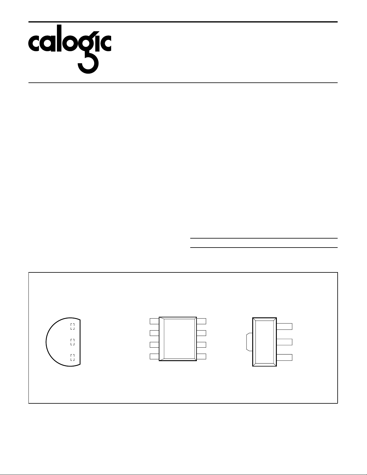
PIN CONFIGU R ATI O N (Top View)
DESCRIPTION
The CL1431 is an adjustable shunt regulator designed t o ac t
as an open-loop error amplifier with a 2.5V temperature
compensated reference. Its highly accurate 0.4% bandgap
reference is perfect for applications requiring stability and
accuracy over temp er atur e and life.
Sharp turn-on characteristics and a low temperature
coefficient make the CL1431 an excellent replacement for
many zener diode applications, programmable to any value
greater than 2.5V and up to 36V by using two external
resistors. As a combination error amplifier and reference, it
can be used to manage contr ol loops suc h a s s w itchin g p ower
supplies.
The CL1431 can be used as a direct replacement for the
standard TL431.
ORDERING INFORMATION
Part Package Temperature Range
o
CL1431LP TO-92 -55 to 125
CL1431D 8-Pin Plastic SOI C -55 to 12 5
CL1431S SOT-89 -55 to 125
C
o
C
o
C
TO-92 (LP)
CATHODE
ANODE
REFERENCE
1G-33
CATHODE
ANODE
ANODE
N/C
SOIC (D)
1
2
3
4
8
REFERENCE
7
ANODE
6
ANODE
5
N/C
1G-34
SOT-89 (S)
CATHODE
ANODE
REFERENCE
1G-35
CALOG IC CORPOR AT ION, 237 Whitney Place, Fremont, California 94539, Telephone: 510-656-2900, FAX: 510-651-3025
CL1431
CORPORATION
ABSOLUTE MAXIMUM RATINGS
SYMBOL PARAMETER RATING UNITS
V
KA
I
AK
I
KA
I
REF
P
D
T
J
T
STG
T
L
Stresses greater than those listed under ABSOLUTE MAXIMUM RATINGS may cause permane nt damag e to the device. This is a stress r ating
only and functional operation of the device at these or any other conditions above those indicated in the operational sections of this specification
is not implied. Exposure to ab solut e ma ximu m rati ng conditi on s for ext ende d peri od s may affe ct reliab ili ty.
RECOMMENDED CONDITIONS
SYMBOL P ARAMETER RATING UNIT
V
KA
I
K
Cathode-Anode Reverse Breakdown 37 V
Anode-Cathode Forward Current 1 A
Operating Cathode Current 250 mA
Reference Inp ut Current 10 mA
Continuous Power Dissipation at 25oC
TO-92
8L SOIC
SOT-89
775
750
1000
Junction Temperature 150
Storage Temperature –65 to 150
Lead Temperature, Soldering 10 Seconds 300
TYPICAL THERMAL RESISTANCES
Cathode Voltage V
to 36 V
REF
Cathode Current 10 mA
PACKAGE θ
TO-92 160
SOIC 175
SOT-89 110
JA
o
C/W 80oC/W 6.3mW/oC
o
C/W 45oC/W 5.7mW/oC
o
C/W 8oC/W 9.1mW/oC
θ
JC
mW
mW
mW
o
C
o
C
o
C
TYPICAL DERATING
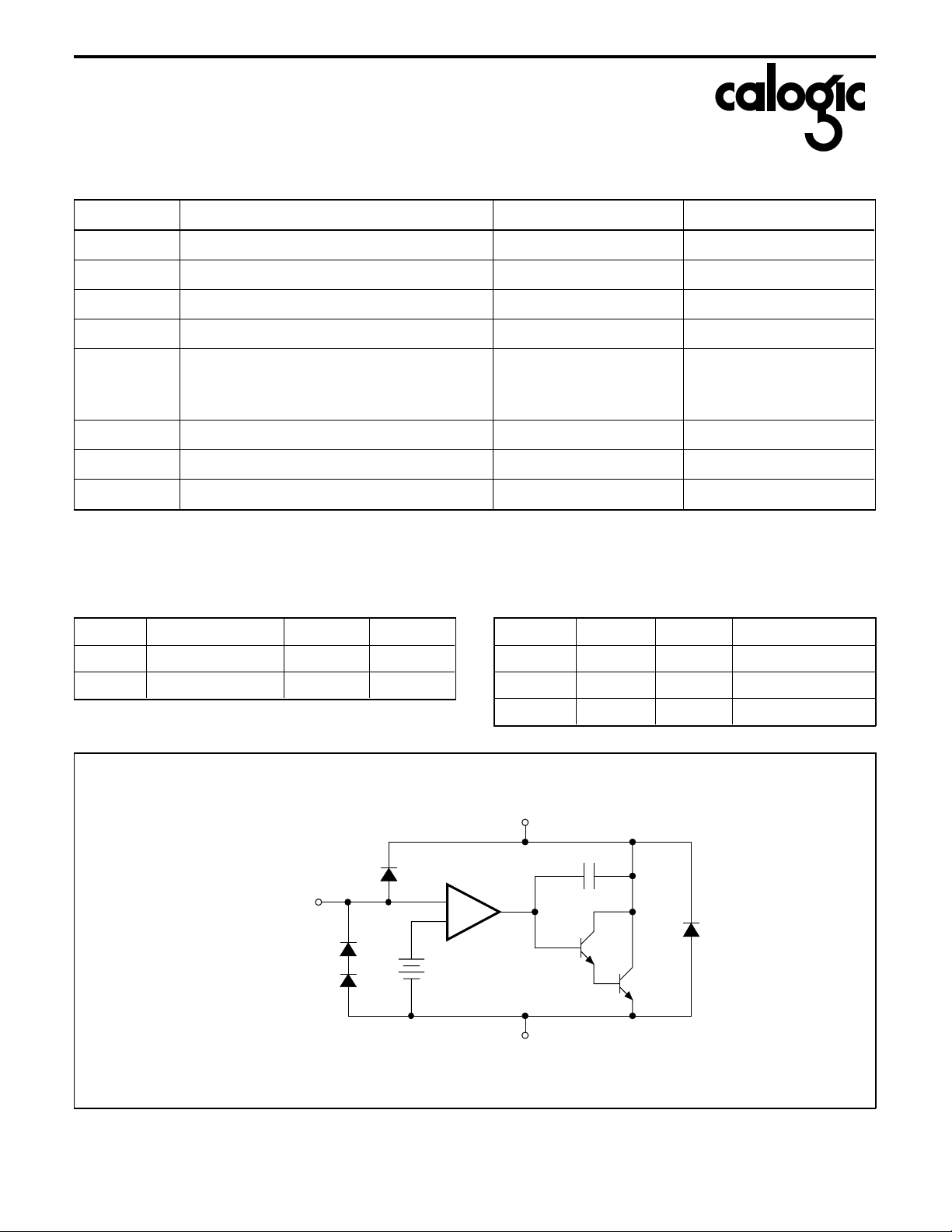
FUNCTIONAL BLOCK DIAGRAM
CATHODE (K)
REFERENCE (R)
+
–
2.5V
ANODE (A)
1G-36
CALOG IC CORPOR ATION, 237 Whitney Place, Fremont, California 94539, T elephone: 510-656-2900, FAX: 510-651-3025
 Loading...