

Calogic LLC 3N191, 3N190 Datasheet
Dual P-Channel
Enhancement Mode MOSFET
General Purpose Amplifier
3N190 / 3N191
FEATURES
••
Ver y High Input Imp edan ce
••
High Gate Breakdown 3N190-3N191
••
Low Capacitance
ABSOLUTE MAXIMUM RATINGS
(T
A
= 25oC unless otherwise specified)
Drain-Source or Drain- Gat e Voltage (Note 1)
3N190, 3N191 . . . . . . . . . . . . . . . . . . . . . . . . . . . . . . . . 40V
Transient Gat e-Sour ce Voltage (Note 1 and 2). . . . . . . ±125V
Gate-Gate Voltage. . . . . . . . . . . . . . . . . . . . . . . . . . . . . . ±80V
Drain Current (Note 1). . . . . . . . . . . . . . . . . . . . . . . . . . 50mA
Storage Tem pe ra tu re. . . . . . . . . . . . . . . . . . . -65
o
C to +200oC
Operating Tem pe ra ture . . . . . . . . . . . . . . . . . -55
o
C to +150oC
Lead Tempera ture (Soldering, 10sec). . . . . . . . . . . . . +300
o
C
Power Dissipation
One Side . . . . . . . . . . . . . . . . . . . . . . . . . . . . . . . . . 300mW
Both Sides . . . . . . . . . . . . . . . . . . . . . . . . . . . . . . . . 525mW
T ot al Der ating abo ve 25
o
C. . . . . . . . . . . . . . . . . . 4.2mW/oC
NOTE: Stresses above those listed under "Absolute Maxi m um
Ratings" may cause permanent damage to the device. These are
stress ratings only and functional operation of the device at these or
any other conditions above those indicated in the operational sections
of the specifications is not implied. Exposure to absolute maximum
rating conditions for extended periods may affect device reliability.
ORDERING INFORMATION
Part Package Temperature Range
3N190-91 Hermetic TO-99 -55
o
C to +150oC
X3N190-91 Sorted Chips in Carriers -55
o
C to +150oC
CORPORATION
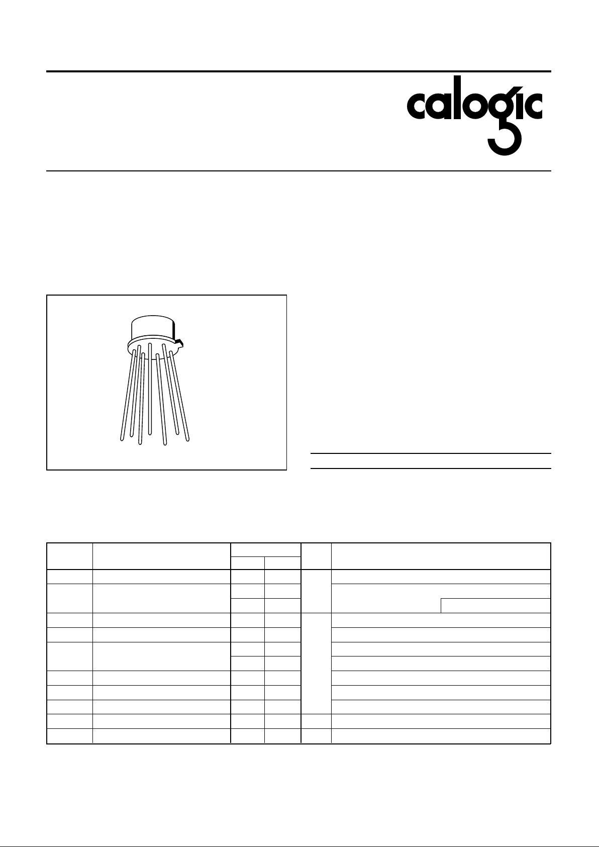
PIN CONFIGU R ATIO N
S2
G1
D2
D1
G2
S1
C
TO-99
2506
ELECTRICAL CHARACTERISTIC S (T
A
= 25oC and VBS = 0 unless otherwise specified)
SYMBOL PARAMETER
3N190/91
UNITS TEST CONDITIONS
MIN MAX
I
GSSR
Gate Reverse Current 10
pA
VGS = 40V
I
GSSF
Gate Forward Current
-10
V
GS
= -40V
-25 T
A
= +12 5oC
BV
DSS
Drain-Source Breakdown Voltage
-40
V
ID = -10µA
BV
SDS
Source-Drain Breakdown Voltage -40 IS = -10µA, VBD = 0
V
GS(th)
Threshold Voltage
-2.0 -5.0
V
DS
= -15V, ID = -10µA
-2.0 -5.0
V
DS
= VGS, ID = -10µA
V
GS
Gate Source Voltage -3.0 -6.5 VDS = -15V, ID = -500µA
I
DSS
Zero Gate Voltage Drain Current
-200
VDS = -15V
I
SDS
Source Drain Current -400 VSD = -15V, VDB = 0
r
DS(on)
Drain-Source on Resistance
300 ohms
VDS = -20V, ID = -100µA
I
D(on)
On Drain Current -5.0 -30.0 mA VDS = -15V, VGS = -10V
3N190 / 3N191
CORPORATION
ELECTRICAL CHARACTERISTIC S (Continued) (TA = 25oC and VBS = 0 unless otherwise specified)
SYMBOL P ARAMETER
3N190/91
UNITS TEST CONDITIONS
MIN MAX
g
fs
Forward Transconductance (Note 3)
1500 4000
µS
V
DS
= -15V, ID = -10mA
f = 1kHz
Y
os
Output Admittance 300
C
iss
Input Capacitance Output Shorted (Note 5) 4.5
pF f = 1MHz
C
rss
Reverse Transfer Capacitance (Note 5) 1.0
C
oss
Output Capacitance Input Shorted (Note 5)
3.0
SWITCHING CHARACTERISTI C S (TA = 25oC and VBS = 0 unless otherwise specified)
SYMBOL PARAMETER MIN MAX UNITS TEST CONDITIONS
t
d(on)
Turn On Delay Time
15
ns V
DD
= -15V, ID = -10mA, RG = RL = 1.4kΩ (Note 5)
t
r
Rise Time
30
t
off
Turn Off Time 50
MATCHING CHARACTERISTICS (TA = 25oC and VBS = 0 unless otherwise specified) 3N188 and 3N190
SYMBOL PARAMETER MIN MAX UNITS TEST CONDITIONS
Y
fs1
/ Y
fs2
Forward Transconductance Ratio
0.85 1.0
VDS = -15V, ID = -500µA, f = 1kHz
V
GS1-2
Gate Source Threshold Voltage Differential
100 mV
VDS = -15V, ID = -500µA
∆V
GS1−2
∆T
Gate Source Threshold Voltage Differential
Change with Temperature (Note 4)
100 µV/
o
C
V
DS
= -15V, ID = -500µA,
T = -55
o
C to +25oC
∆V
GS1−2
∆T
Gate Source Threshold Voltage Differential
Change with Temperature (Note 4)
100 µV/
o
C
V
DS
= -15V, ID = -500µA
T = +25
o
C to +125oC
NOTES: 1. Per transistor.
2. Approximately doubles for every 10
o
C increase in TA.
3. Pulse test duration = 300µs; duty cycle ≤3%.
4. Measured at end points, T
A
and TB.
5. For design reference only, not 100% tested.
 Loading...