

Calogic LLC 3N173, 3N172 Datasheet
Diode Protected P-Channel
Enhancement Mode MOSFET
General Purpose Amplifier/Switch
3N172 / 3N173
FEATURES
••
High Input Impedance
••
Diode Protected Gate
ABSOLUTE MAXIMUM RATINGS
(T
A
= 25oC unless otherwise specified)
Drain-Source or Dr ain- Gat e V olta ge
3N172. . . . . . . . . . . . . . . . . . . . . . . . . . . . . . . . . . . . . . . 40V
3N173. . . . . . . . . . . . . . . . . . . . . . . . . . . . . . . . . . . . . . . 30V
Drain Current. . . . . . . . . . . . . . . . . . . . . . . . . . . . . . . . . 50mA
Gate Forward Current . . . . . . . . . . . . . . . . . . . . . . . . . . . 10µA
Gate Reverse Current . . . . . . . . . . . . . . . . . . . . . . . . . . . 1mA
Storage Temperatur e . . . . . . . . . . . . . . . . . . -65
o
C to +200oC
Operating Temperature . . . . . . . . . . . . . . . . . -55
o
C to +150oC
Lead Temperature (Soldering, 10sec). . . . . . . . . . . . . +300
o
C
Power Dissipation . . . . . . . . . . . . . . . . . . . . . . . . . . . . 375mW
Derate above 25
o
C . . . . . . . . . . . . . . . . . . . . . . . 3.0mW/oC
NOTE: Stresses above those listed under "Absolute Maxi mum
Ratings" may cause permanent damage to the device. These are
stress ratings only and functional operation of the device at these or
any other conditions above those indicated in the operational sections
of the specifications is not implied. Exposure to absolute maximum
rating conditions for extended periods may affect device reliability.
ORDERING INFORMATION
Part Package Temperature Range
3N172-73 Hermetic TO-72 -55
o
C to +150oC
X3N172-73 Sorted Chips in Carriers -55
o
C to +150oC
CORPORATION
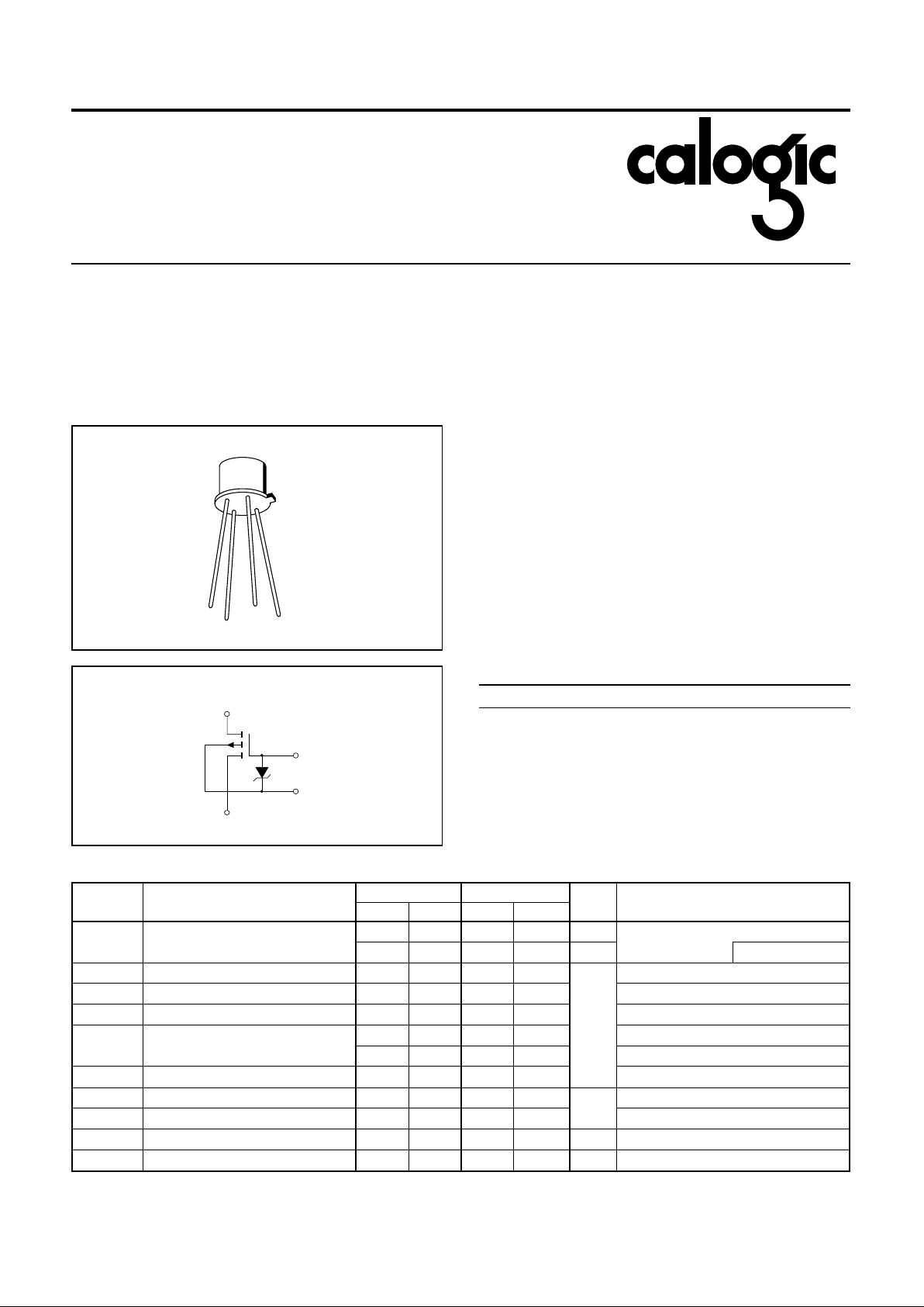
PIN CONFIGU R ATION
TO-72
G
D
S
C,B
1503Z
DEVICE SCHEMATIC
1
2
0200
3
4
ELECTRICAL CHARACTERISTIC S (TA = 25oC and VBS = 0 unless otherwise specified)
SYMBOL PARAMETER
3N172 3N173
UNITS TEST CONDITIONS
MIN MAX MIN MAX
I
GSS
Gate Reverse Current
-200 -500 pA V
GS
= -20V
-0.5 -1.0 µA
T
A
= +1 25oC
BV
GSS
Gate Breakdown Voltage -40 -125 -30 -125
V
ID = -10µA
BV
DSS
Drain-Source Breakdown Voltage -40 -30 ID = -10µA
BV
SDS
Source-Drain Breakdown Voltage
-40 -30
IS = -10µA, VDB = 0
V
GS(th)
Threshold Voltage
-2.0 -5.0 -2.0 -5.0 V
DS
= VGS, ID = -10µA
-2.0 -5.0 -2.0 -5.0 V
DS
= -15V, ID = -10µA
V
GS
Gate Source Voltage
-3.0 -6.5 -2.5 -6.5
VDS = -15V, ID = -500µA
I
DSS
Zero Gate Voltage Drain Current -0.4 -10
nA
VDS = -15V, VGS = 0
I
SDS
Zero Gate Voltage Source Current -0.4 -10 VSD = -15V, VDB = 0, VGD = 0
r
DS(on)
Drain Source On Resistance
250 350 ohms
VGS = -20V, ID = -100µA
I
D(on)
On Drain Current -5.0 -30 -5.0 -30 mA VDS = -15V, VGS = -10V
3N172 / 3N173
CORPORATION
SMALL-SIGNAL ELECTRICAL CHARACTERISTICS TA = 25oC and Bulk (substrate) Lead Connect ed to Source
SYMBOL P ARAMETER
3N172 3N173
UNITS TEST CONDITIONS
MIN MAX MIN MAX
| y
fs
|
Magnitude of Small-Signal, Common-Source,
Short-Circuit, Forward Transadmittance*
1500 4000 1000 4000 µSV
DS
= -15V, ID = -10mA, f = 1kHz
| y
os
|
Magnitude of Small-Signal, Common-Source,
Short-Circuit, Output Admittance*
250 250 µS
V
DS
= -15V, ID = -10mA, f = 1kHz
C
iss
Small-Signal, Common-Source, Short-Circuit,
Input Capacitance*
3.5 3.5 pF V
DS
= -15V, ID = -10mA, f = 1MHz
C
rss
Small-Signal, Common-Source, Short-Circuit,
Reverse Transfer Capacitance*
1.0 1.0 pF
V
DS
= -15V, ID = -10mA, f = 1MHz
C
oss
Small-Signal, Common-Source, Short-Circuit,
Output Capacitance*
3.0 3.0 pF V
DS
= -15V, ID = -10mA, f = 1MHz
NOISE CHARACTERISTICS
SYMBOL PARAMETER TYPICAL UNITS TEST CONDITIONS
NF Common-Sou r ce Spot Noise Fig ure
1.0 dB
V
DS
= -15V, ID = -1mA, f = 1kHz, RG = 1MΩ
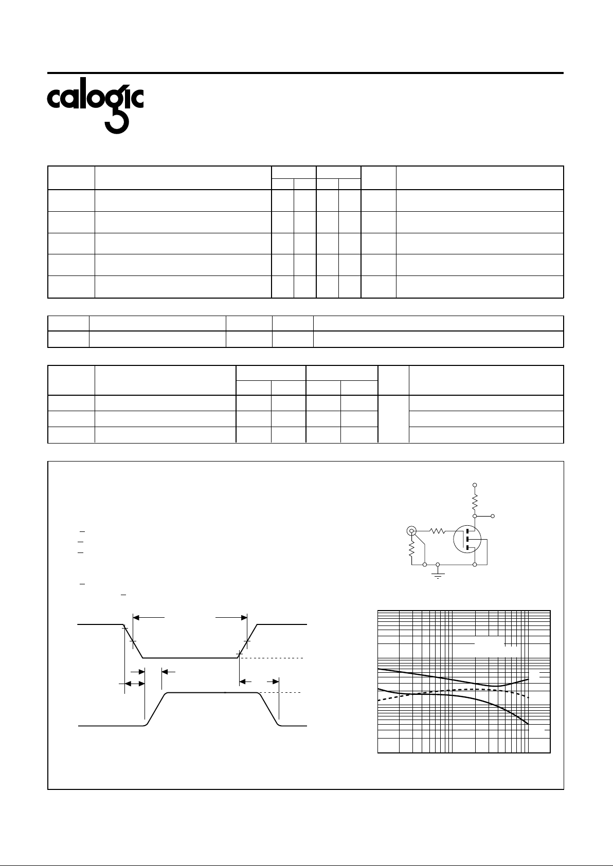
SWITCHING CHARACTERISTI C S TA = 25oC Bulk (substrat e) Lead Con nect ed to Sou rce
SYMBOL PARAMETER
3N172 3N173
UNITS TEST CONDITIONS
MIN MAX MIN MAX
t
d (on)
Turn-On Delay Time* 12 12
ns
VDD = -15V, I
D (on)
= -10mA
t
r
Rise Time* 24 24 RG = RL = 1.4kΩ
t
off
Turn-Off Delay Time*
50 50
See Test Circuit Below
*Registered JEDEC Data
SWITCHING TIME D ETAIL
-0V
-1V
-15V
10%
50% 50%
90%
90%
10%
PULSE
WIDTH
90%
0210
MEASUREMENTS ON SAMPLING OSCILLOSCOPE WITH
INPUT PULSE
rise
t < 2ns
PULSE WIDTH
rise
t < 0.2ns
in
C
in
R
V
IN
V
OUT
4(on)
t
r
t
off
t
IN
-V
> 200ns
< 2.0pF
> 10MΩ
0220
D.U.T.
V
DD
R
L
V
OUT
R
G
50Ω
V
IN
-0.1 -0.5 -1.0 -5.0 -10
SWITCHING TIS - nSEC
SWITCHING TIMES vs. ON-STATE
DRAIN CURRENT
ON-STATE DRAIN CURRENT - (I
D(on)
) - mA
t
d(on)
rise
t
off
G
= RL= 1.4KR
VDD= 15V
0230
1000
500
1.0
t
5.0
100
50
10
 Loading...