

Calogic LLC 3N171, 3N170 Datasheet
N-Channel Enhancement
Mode MOSFET Switch
3N170 / 3N171
FEATURES
••
Low Switching Voltages
••
Fast Switching Times
••
Low Drain-Source Resistance
••
Low Reverse Transfer Capac itance
HANDLING PRECAUTIONS
MOS field-effect transistors have extremely high input
resistance and can be damaged by the accumulation of
excess static charge. To avoid possible dam age to the dev ice
while wiring, testing, or in actual operation, follow the
procedures outlined below .
1. To avoid the build-up of static charge, the leads of the
devices should remain shorted together with a metal ring
except when being te sted or used.
2. Avoid unnecessary handling. Pick up devices by the case
instead of the leads.
3. Do not insert or remove devices from circuits with the
power on as transient voltages may cause permanent
damage to the devices.
ABSOLUTE MAXIMUM RATINGS
(T
A
= 25oC unless otherwise specified)
Drain-Gate Voltage . . . . . . . . . . . . . . . . . . . . . . . . . . . . . ±35V
Drain-Source Voltage. . . . . . . . . . . . . . . . . . . . . . . . . . . . . 25V
Gate-Source V o ltage. . . . . . . . . . . . . . . . . . . . . . . . . . . . ±35V
Drain Current. . . . . . . . . . . . . . . . . . . . . . . . . . . . . . . . . 30mA
Storage Temperatur e Ra nge. . . . . . . . . . . . . -65
o
C to +200oC
Operating Temperatur e Ra nge . . . . . . . . . . . -55
o
C to +150oC
Lead Temperature (Soldering, 10se c). . . . . . . . . . . . . +300
o
C
Power Dissipation . . . . . . . . . . . . . . . . . . . . . . . . . . . . 300mW
Derate above 25
o
C . . . . . . . . . . . . . . . . . . . . . . . 2.4mW/oC
NOTE: Stresses above those listed under "Absolute Maxi m um
Ratings" may cause permanent damage to the device. These are
stress ratings only and functional operation of the device at these or
any other conditions above those indicated in the operational sections
of the specifications is not implied. Exposure to absolute maximum
rating conditions for extended periods may affect device reliability.
ORDERING INFORMATION
Part Package Temperature Range
3N170-71 Hermetic TO-72 -55
o
C to +150oC
X3N170-71 Sorted Chips in Carriers -55
o
C to +150oC
CORPORATION
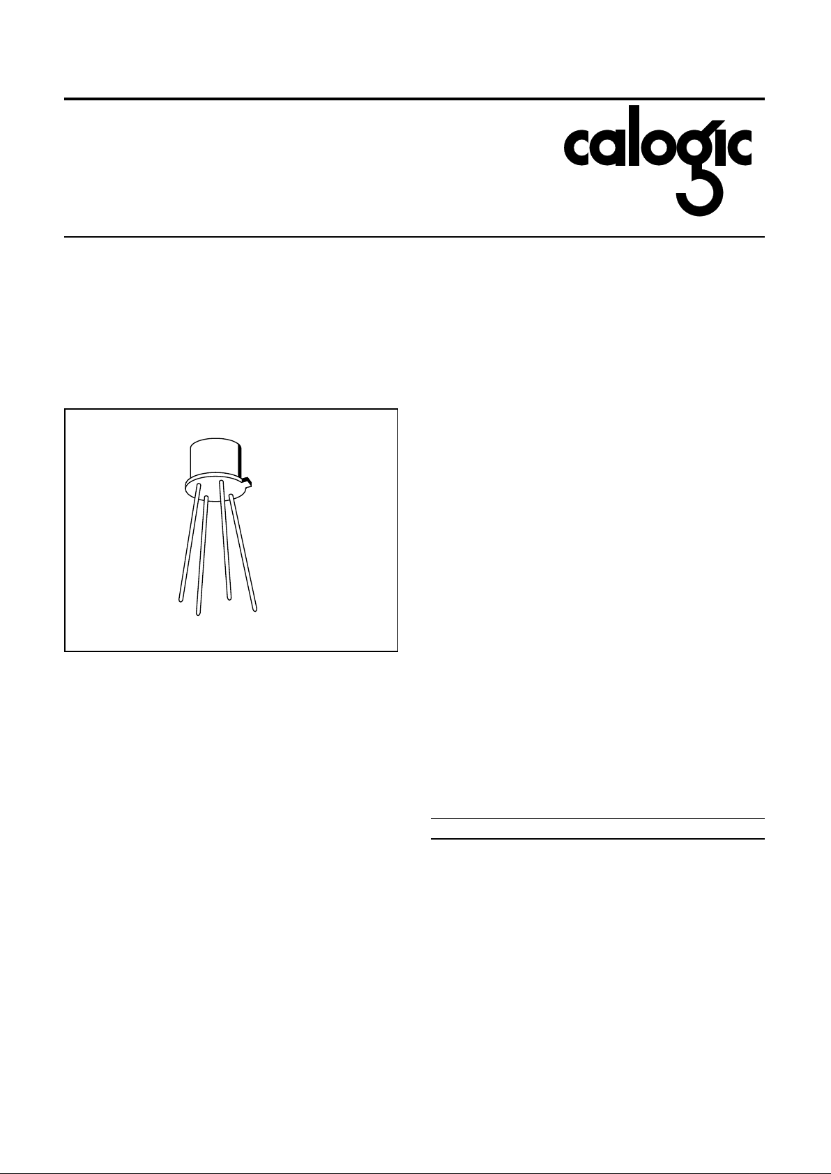
PIN CONFIGU R ATION
TO-72
G
D
S
C,B
1003

ELECTRICAL CHARACTERISTIC S (TA = 25oC unless otherwise sp ecif ied) Substr ate conn ected t o sourc e.
SYMBOL PARAMETER MIN MAX UNITS TEST CONDITIONS
BV
DSS
Drain-Source Breakdown Voltage
25 V
ID = 10µA, VGS = 0
I
GSS
Gate Leakage Current
±10
pA
V
GS
= ±35V, VDS = 0
100 VGS = 35V, VDS = 0, TA = 125oC
I
DSS
Zero-Gate-Voltage Drain Current
10 nA V
DS
= 10V, VGS = 0
1.0 µA
T
A
= 125oC
V
GS(th)
Gate-Source Threshold Voltage
3N170
1.0 2.0
VVDS = 10V, ID = 10µA
3N171
1.5 3.0
I
D(on)
"ON" Drain Current 10 mA VGS = 10V, VDS = 10V
V
DS(on)
Drain-Source "ON" Voltage 2.0 V ID = 10mA, VGS = 10V
r
ds(on)
Drain-Source ON Resistance
200 Ω
VGS = 10V, ID = 0, f = 1kHz
| Yfs | Forward Transfer Admittance
1000 µS
VDS = 10V, ID = 2.0mA, f = 1kHz
C
rss
Reverse Transfer Capacitance (Note 1)
1.3
pF
VDS = 0, VGS = 0, f = 1MHz
C
iss
Input Capacitance (Note 1) 5.0 VDS = 10V, VGS = 0, f = 1MHz
C
d(sub)
Drain-Substrate Capacitance (Note 1) 5.0 V
D(SUB)
= 10V, f = 1MHz
t
d(on)
Turn-On Delay Time (Note 1)
3.0
ns
VDD = 10V, I
D(on)
= 10mA ,
V
GS(on)
= 10V, V
GS(off)
= 0,
R
G
= 50Ω
t
r
Rise Time (Note 1)
10
t
d(off)
Turn-Off Delay Time (Note 1) 3.0
t
f
Fall Time (Note 1) 15
NOTE 1: For design reference only, not 100% tested.
3N170 / 3N171
CORPORATION
 Loading...