

Calogic SST5911 Datasheet
N-Channel JFET
Monolithic Dual
SST5911 / SST5912
CORPORATION
FEATURES
High Gain . . . . . . . . . . . . . . . . . . . . . . . . . . . . . . gfs > 6 mS
••
Low Leakage . . . . . . . . . . . . . . . . . . . . . . IG < 1pA typical
••
Low Noise
••
Surface Mou nt Package
••
APPLICATIONS
Differential Wi de band Amplifier
••
VHF/UHF Amplifie rs
••
T est and Measu rement
••
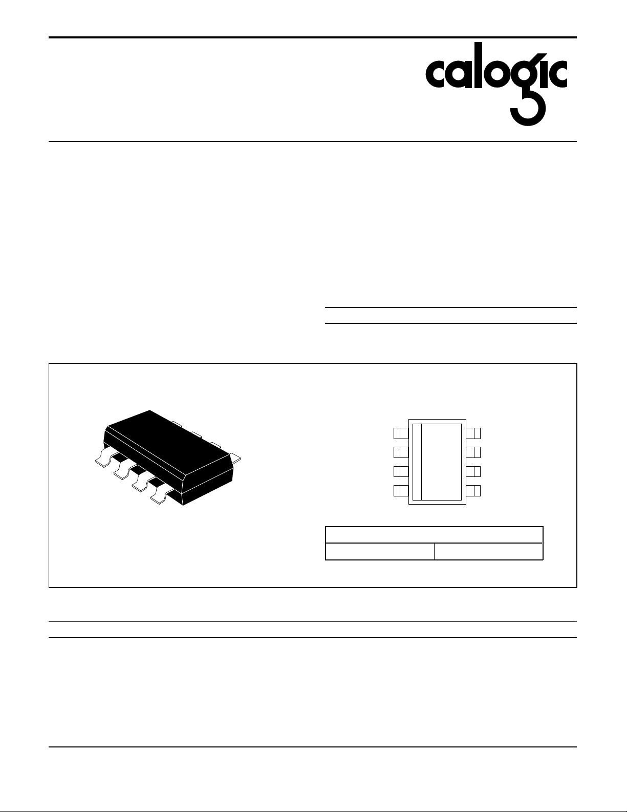
PIN CONFIGU R ATI O N
SO-8
DESCRIPTION
The SST5912 is a High Speed N-Channel Monolithic JFET
pair encapsulated in a surface mount plastic SO-8 package.
The device is designed for high gain (typically > 600 0 µmhos),
low leakage ( < 1pA typically) and low noise, The SST5912 is
an excellent choice for differential wideband amplifiers,
VHF/UHF amplifiers and test and mea sur emen t.
ORDERING INFORMATION
Part Package Temperature Range
o
SST5912 Plastic SO-8 Package -55
NOTE: For Sorted Chips in Carriers, See 2N5911 Series
TOP VIEW
(1) S1
(2) D1
(3) G1
(4) N/C
C to +150oC
N/C (8)
G2 (7)
D2 (6)
S2 (5)
CJ1
PRODUCT MARKING
SST5912 SST5912
ABSOLUTE MAXIMUM RATINGS (TA = 25oC unless otherwise noted)
Parameter/Test Conditio n Symbol Limit Unit
Gate-Drain Voltage V
Gate-Source Voltage V
Forward Gate Cur r ent I
Power Dissipation (per side) P
(total) 500 mW
Power Derating (per side) 2.4 mW/
(total) 4 mW/
Operating J unct ion Temper at ur e T
Storage Tempera ture T
Lead Temperature (1/ 16 " fr om case for 10 seconds) T
GD
GS
G
D
J
stg
L
-25 V
-25 V
50 mA
300 mW
-55 to 150
-65 to 150
300
o
C
o
C
o
C
o
C
o
C
CORPORATION
ELECTRICAL CHARACTERISTIC S (TA = 25oC unless otherwise note d)
SST5912
SYMBOL CHARACTERISTCS TYP
STATIC
V
(BR)GSS
) Gate-Source Cut off Voltage -3.5 -1 -5 VDS = 10V, ID = 1nA
V
GS(OFF
I
DSS
I
GSS
I
G
V
GS
V
GS(F)
Gate-Source Breakdown Voltage -35 -25
Saturation Drain Current
2
Gate Reverse Current
Gate Operating Current
Gate-Source Voltage -1.5 -0.3 -4
Gate-Source Forward Voltage 0.7 IG = 1mA, VDS = 0V
DYNAMIC
g
fs
g
os
g
fs
g
os
C
iss
C
rss
e
n
Common-Source Forward Transconductance 6 5 10 mS
Common-Source Output Conductance 20 100 µS
Common-Source Forward Transconductance 6 5 10 mS
Common-Source Output Conductance 30 150 µS
Common-Source Input Capacitance 3.5 5
Common-Sourc e Revers e T rans f er Capac it anc e 1 1.2
Equivale nt Inp ut Noise Voltage 4 20 nV/ Hz VDG = 10V, ID = 5mA, f = 10kHz
NF Noise Figure 0.1 1 dB V
1
MIN MAX
UNIT TEST CONDITIONS
V
15 7 40 mA VDS = 10V, VGS = 0V
-1 -100 pA V
-0.2 nA T
-1 -100 pA V
-0.2 nA T
V
pF
SST5911 / SST5912
IG = -1µA, VDS = 0V
= -15V, VDS = 0V
GS
= 125oC
A
= 10V, ID = 5mA
DG
= 125oC
A
VDG = 10V, ID = 5mA
V
= 10V, ID = 5mA
DG
f = 1kHz
V
= 10V, ID = 5mA
DG
f = 100MHz
V
= 10V, ID = 5mA
DG
f = 1MHz
= 10V, ID = 5mA, f = 10kHz, RG = 100Ω
DG
ELECTRICAL CHARACTERISTIC S (continued) (TA = 25oC unless otherwise noted)
SYMBOL CHARACTERISTICS
| I
- I
| Di ffere ntial Gate Current 20 20 n A VDG = 10V, ID = 5mA TA = 125oC
G1
G2
I
| V
∆ | V
GS1
I
GS1
DSS1
DSS2
- V
- V
g
fs1
g
fs2
Saturation Drain Current Ratio 0.95 1 0.95 1
| Differential Gate-Source Voltage 10 15 mV
GS2
|∆TGate Source Voltage Differential Drift
GS2
(Measured at end points, T
and TB)
A
Transconducta nce Rati o 0.95 1 0.9 5 1 f = 1kHz
NOTES: 1 . For design aid only, not subject to produ ct ion test ing .
2. Pulse test; PW = 300µs, duty cycle ≤ 3%.
SST5911 SST5912
MIN MAX MIN MAX
20 40
20 40
UNITS TEST CONDITIONS
VDS = 10V, V
GS
= 0
(Pulsewidth 300µs, duty cycle ≤ 3%)
= 25oC
T
A
T
= 125oC
µV/
o
C
= 10V, ID = 5mA
V
DG
B
T
= -55oC
A
T
= 25oC
B
 Loading...