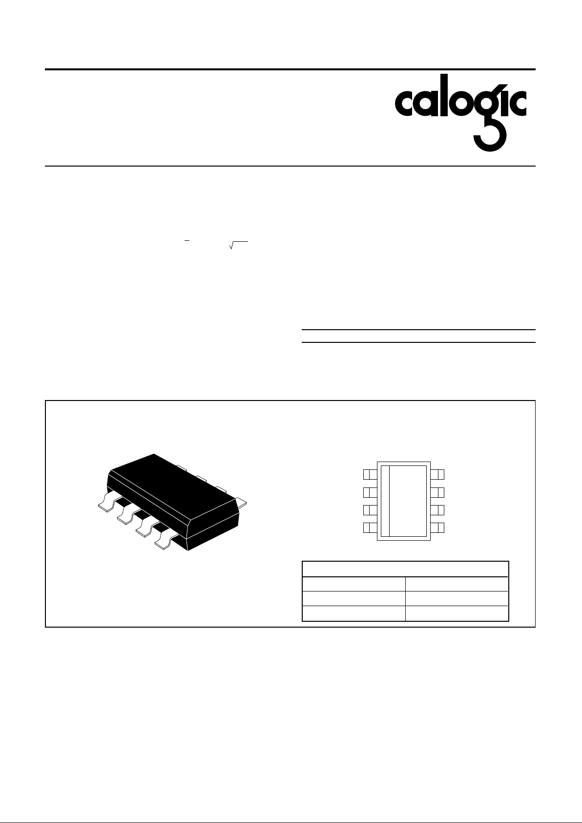
Calogic SST406, SST405, SST404 Datasheet

N-Channel JFET
Monolithic Dual
SST404 / SST405 / SST406
FEAT URES
••
V ery Low Noi se . . . . . . . . . . . . . en < 10 nV/ Hz @ 10Hz
••
Low Input Bia s. . . . . . . . . . . . . . . . . . . . . . . . . . . IG < 2pA
••
High Breakdown Voltage. . . . . . . . . . . . . . . . . . . BV > 50V
APPLICATIONS
••
Precision I nst ru me nta tio n
••
Inp ut Ampl if iers
••
Impedance Converters
DESCRIPTION
The SST404 Series is a very Low Noise Monolithic
N-Channel JFET Pair in a surface mount SO-8 plastic
package. Designed utilizing Calogic’s proprietary JFET
processing techniques these devices are ideal for front end
amplification of low level signals. The low noise, low leakage
and good frequency response are excellent features for
sensitive medical, inst rument ation an d infrared de signs .
ORDERING INFORMATION
Part Package Tempe rature Range
SST404-6 Plastic SO-8 -55
o
C to +125oC
NOTE: For Sorted Chips in Carriers, See U401 Series
PIN CONFIGU RATIONS
CORPORATION
SO-8
TOP VIEW
(1) S1
(2) D1
(3) G1
(4) N/C
N/C (8)
G2 (7)
D2 (6)
S2 (5)
CJ2
PRODUCT MARKING
SST404 R04
SST405 R05
SST406 R06

SST404 / SST405 / SST406
CORPORATION
ABSOLUTE MAXIMUM RATINGS (TA = 25oC unless otherwise no ted)
Param ete r/Test Condition Symbol Limit Unit
Gate-Drain Voltage V
GD
-50 V
Gate-Source V olta ge V
GS
-50 V
Forward Gate Current I
G
10 mA
Pow er Dissipation (per side) P
D
300 mW
(total) 500 mW
Pow er Der ati ng (per side) 2.4 mW/
o
C
(total) 4 mW/
o
C
Operating Junc tion Temperature T
J
-55 to 150
o
C
Storage Temperat ure T
stg
-55 to 200
o
C
Lead Temperature (1/16" from case f or 1 0 seconds ) T
L
300
o
C
ELECTRICAL CHARACTERIST ICS (TA = 25oC unless otherwise noted)
SYMBOL CHARACTERISTCS TYP
1
SST404 SST405 SST406
UNIT TEST CONDITIONS
MIN MAX MIN MAX MIN MAX
STATIC
V
(BR)GSS
Gate-Source Breakdown Voltage -58 -50 -50 -50
V
I
G
= -1µA, VDS = 0V
V
(BR)G1 - G2
Gate-Gate Breakdown Voltage -58
±50 ±50 ±50 I
G
= ±1µA, VDS = 0V, VGS = 0V
V
GS(OFF
) Gate-Source Cut off Voltage -1.5 -0.5 -2.5 -0.5 -2.5 -0.5 -2.5 VDS = 15V, ID = 1nA
I
DSS
Saturation Drain Current
2
3.50.5100.5100.510 mA VDS = 15V, VGS = 0V
I
GSS
Gate Reverse Current
-2 -25 -25 -25 pA V
GS
= -30V, VDS = 0V
-1 nA T
A
= 125oC
I
G
Gate Operating Current
-2 -15 -15 -15 pA
V
DG
= 15V, ID = 200µA
-0.8 -10 -10 -10 nA T
A
= 125oC
r
DS(ON)
Drain-Source On-Resistance 250
Ω
VGS = 0V, ID = 0.1mA
V
GS
Gate-Source Voltage -1 -2.3 -2.3 -2.3
V
V
DG
= 15V, ID = 200µA
V
GS(F)
Gate-Source Forward Voltage 0.7 IG = 1mA, VDS = 0V
DYNAMIC
g
fs
Common-Source Forward Transconductance 1.5 121212 mS
VDG = 15V, I
D
= 200µA
f = 1kHz
g
os
Common-Source Output Conductance 1.3 2 2 2
µS
g
fs
Common-Source Forward Transconductance 1.5 272727
VDS = 10V, V
GS
= 0V
f = 1kHz
g
os
Common-Source Output Conductance 10 20 20 20
C
iss
Common-Source Input Capacitance 8 8 8
pF
V
DG
= 15V, ID = 200µA
f = 1MHz
C
rss
Common-Source Reve rse Transfer Capacitance 1.5 3 3 3
e
n
Equivalent Input Noise Voltage 10 20 20 20 nV/ Hz
V
DG
= 15V, ID = 200µA
f = 10Hz
MATCHING
| V
GS1
- V
GS2
| Differential Gate-Source Voltage 15 20 40 mV
V
DG
= 10V, ID = 200µA
∆ | V
GS1
- V
GS2
|∆TGate-Source V oltage Differential Change with
Temperature
25 40 80
µV/
o
C
T
A
= -55 to 25oC
V
DG
= 10V,
I
D
= 200µA
25 40 80 T
A
= 25 to 125oC
CMRR Common Mode Rejection Ratio 102 95 90 dB
V
DG
= 10 to 20V, ID = 200µA
NOTES: 1. For design aid only, not subject to production testing.
2. Pulse test; PW = 300µs, duty cycle ≤ 3%.
 Loading...