

查询LH4002供应商
Wideband Video Buffer
LH4002A / LH4002 / LH4002C
CORPORATION
FEATURES
DC to 300 MHz Ban dw idt h w ith VS = ±5V
••
3000 V/µs Slew Rat e i nt o 5 0Ω
••
APPLICATIONS
Wideband Amp lifier Buffer
••
Wideb and Lin e Driver
••
Video
••
Coaxial Cable Driver
••
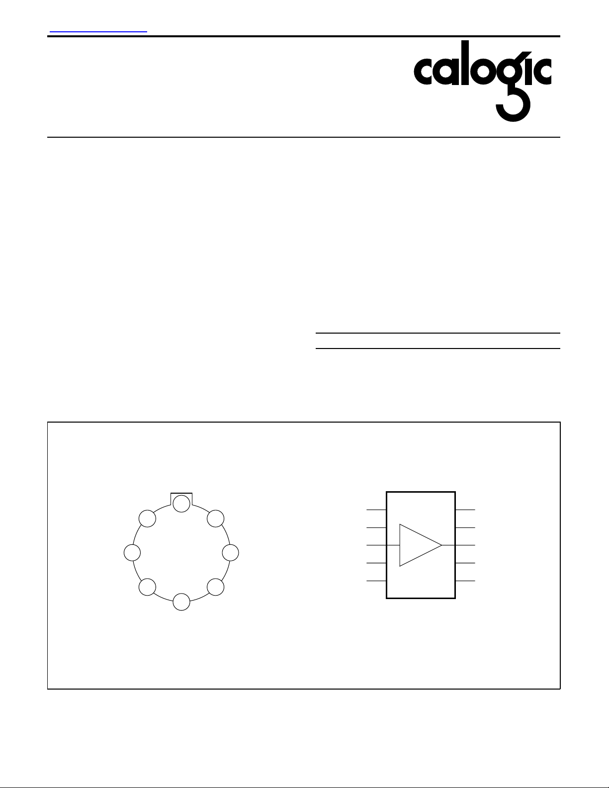
CONNECTION DIAGRAMS
METAL CA N PACKAGE
INPUT
GENERAL DESCRIPTION
The LH4002 family is a high speed voltage follower designed
to drive video signals from DC up to 300MHz. At voltage
supplies of ±5V, the LH4002 family will provide up to 80mA
into 50Ω at slew rates of 2000 V/µs.
The LH4002 family is intended to fulfill a wide range of high
speed applications including video distribution, impedance
transformation, and load isolation. It is also suitable for use in
current boost er appl ications within an op amp loop. This allows
the output current capability of existing op amps to be increased.
ORDERING INFORMATION
Part Package Temperature Range
o
LH4002AH HO8A (TO5-8 Le ad) -55
LH4002H HO8A (TO 5-8 Le ad) -55
LH4002CH HO8A (TO5-8 Lead) -40
LH4002AN N10A (P lastic Dip- 10 Lead) -40
LH4002N N10A (P lastic Dip- 10 Lead) -40
LH4002CN N10A (Plastic Dip-10 Lead) -40
DUAL-IN-LINE
PACKAGE
C to +125oC
o
C to +125oC
o
C to +85oC
o
C to +85oC
o
C to +85oC
o
C to +85oC
+V
+V
CC2
CC1
NC
8
-V
7
6
5
4
OUTPUT
HO8A
1
CC1
-V
2
CC2
3
NC
+V
+V
-V
-V
1
CC2
2
CC1
3
4
CC1
56
CC2
TOP VIEW
N10A
10
9
8
7
E
1
E
3
OUTPUTINPUT
E
4
E
2
CALOGIC CORPORATION, 237 Whitney Plac e, Fremont, C alifornia 9453 9, Telephone: 510-656-29 0 0, FAX: 510-651- 10 76
CORPORATION
ABSOLUTE MAXIMUM RATINGS (Note 1)
Supply Voltage. . . . . . . . . . . . . . . . . . . . . . . . . . . . . . . . . . ±10
Input Voltage . . . . . . . . . . . . . . . . . . . . . . . . . . . . . . ±Vsupply
Storage Temperature Ra nge. . . . . . . . . . . . -65
Lead Temper at ur e
(Soldering 10 se conds) . . . . . . . . . . . . . . . . . . . . . . 260
o
C to +150oC
o
Power Dissipation . . . . . . . . . . . . . . . . . . . . . . . . . . . (Note 4)
LH4002A / LH4002 / LH4002C
ESD Tolerance (Note 3). . . . . . . . . . . . . . . . . . . . . . . ±2000V
Therma l Re sistance (θ
H Package . . . . . . . . . . . . . . . . . . . . . . . . . . . . . . 125
N Package . . . . . . . . . . . . . . . . . . . . . . . . . . . . . . . 50
C
Maximum J unction Temperature . . . . . . . . . . . . . . . . . . 150
) (Note 6)
JA
o
C/W
o
C/W
o
C
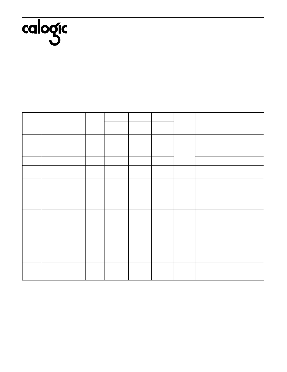
DC ELECTRICAL CHARACTERISTICS
The following specifications apply for Supply Vo ltag e = ±5V, V
Boldface limits apply for T
= TJ = T
A
SYMBOL CHARACTERISTICS TYP
A
V1
A
V2
A
V3
V
OS
I
B
R
IN
C
IN
R
O
I
S1
Voltage Gain 1 0.99
Voltage Gain 2 0.92 0.89 0.88 0.87 RL = 50Ω, VIN = ±3V
Voltage Gain 3 0.92 0.89 0.87 0.87 RL = 50Ω, VIN = ±2V
Offset Voltage 10
Input Bias Current 1
Input Resistance 0.3 MΩ RS = 10K, RL = 50Ω
Input Capacitance 3.5 pF
Output Resistance 3
Supply Current 1 20
MIN
to T
; all other limits TA = TJ = 25oC.
MAX
LH4002A LH4002 LH4002C
Limit
(Note 5)
0.96
0.95
15
25
10
20
10
10
30
35
= 0, RL ≥ 100KΩ and RS = 50Ω unless oth er w ise noted.
CM
Limit
(Note 5)
0.95
0.95
Limit
(Note 5)
0.95
0.95
UNITS CONDITIONS
R
= 1K, VIN = ±2V, RS = 10K
L
V/V Min
25
35
15
30
10
10
30
35
30
40
20
40
10
10
35
35
mV Max R
µA Max R
Ω Max R
mA Max R
= 50Ω, RS = 150Ω
L
= 50Ω, RS = 1KΩ
L
= 10K, RL = 50Ω
S
= 10K, VIN = 0V, RL = 1K
S
V
O1
Output Swing 1 2.4
2.2
2.2
2.2
2.2
2.2
2.2
R
= 150Ω, VIN = ±2.5V, RL = 50Ω
S
±V Min
V
V
I
O2
O3
OUT
Output Swing 2 2.2
2
2
Output Swing 3 3.6 3.0 3.0 3.0 VPP Min RS = 150Ω, VIN = ±4.5V, RL = 50Ω
Output Current 80 60 60 60 mA VIN = 4V
2
2
2
2
R
= 150Ω, VIN = ±2.5V, RL = 1K
S
CALOGIC CORPORATION, 237 Whitney Plac e, Fremont, C alifornia 9453 9, Telephone: 510-656-29 0 0, FAX: 510-651- 10 76

LH4002A / LH4002 / LH4002C
CORPORATION
AC ELECTRICAL CHARACTERISTICS
The following specifications apply for Supply Vo ltag e = ±5V, V
Boldface limits apply for T
= TJ = T
A
SYMBOL CHARACTERISTICS TYP
SR
SR
SS
LS
P
BW
tr, t
t
pd
O
1
2
BW
BW
f
S
Slew Rate 1 3000 2750 2500 2500
Slew Rate 2 2000 1750 1600 1500 VIN = ±4V, RL = 50Ω (Note 2)
Small Signal
Bandwidth
Large Signal
Bandwidth
Power Bandwidth 130 100 90 80 RL = 50Ω, V
Rise Time
Fall Time
Propagation Delay
Time
Overshoot 10 %
Note 1: Absolute Maximu m Rating s indicate limits beyond which dama ge to the device may occur. DC and AC electrical specification s do no t
apply when operating the device beyond its rated operating condition s.
Note 2: Slew rate is measured with 50Ω so urce imped an ce at 25
5000V/µs.
Note 3: The test circuit consists of the human body model of 120pF in series with 1500Ω.
Note 4: The maximum power dissipation is a function of T
temperature is P
D
= (T
J(max)
- TA)/θJA.
Note 5: Limits are guaranteed by testing, correlation or periodic characterization.
Note 6: For N package, θ
is measured by soldering the unit directly on a printed circuit board and V- pins are connected to 2 square inches of 2
JA
oz copper.
MIN
to T
; all other limits TA = TJ = 25oC.
MAX
LH4002A LH4002 LH4002C
Limit (Note 5) Limit (Note 5) Limit (Note 5)
300 250 220 200
140 100 90 80 R
1.2 1.5 1.7 1.8 ns
2.0 ns
J(max), θJA
= 0, RL ≥ 100KΩ and RS = 50Ω unless oth er w ise noted.
CM
UNITS CONDITIONS
V/µs
MHz
o
C. For accurate measurements, the input slew rate should be at least
VIN = ±2V, RL = 50Ω (Note 2)
R
= 50Ω, V
L
= 50Ω, V
L
R
= 50Ω, CL ≤ 10pF
L
V
= 100mV
O
R
= 50Ω, CL ≤ 10pF
L
V
= 100mV
O
R
= 50Ω, CL ≤ 10pF
L
V
= 100mV
O
= 100mV
OUT
= 2V
OUT
= 4V
OUT
PP
PP
PP
P-P
P-P
and TA. The maximum allowable power dissipation at any ambient
P-P
CALOGIC CORPORATION, 237 Whitney Plac e, Fremont, C alifornia 9453 9, Telephone: 510-656-29 0 0, FAX: 510-651- 10 76

CORPORATION
TYPICAL PERFORMANCE CHARACTERI STI CS
LH4002A / LH4002 / LH4002C
FREQUENCY RESPONSE
20
15
10
5
0
-5
RL= 100Ω
-10
GAIN (dB)
V
≤ 100mV
IN
-15
C
≤ 100pF
L
-20
T
= 25˚C
j
-25
-30
0.5 51 2 10 20 20050 100 1000500
FREQUENCY (MHz)
BANDWIDTH
(LARGE SIGNAL & POWER)
10
P-P
(V )
OUT
V
9
8
7
6
5
4
3
2
1
0
11025
RL= 100Ω
R
L
20 50 400100 200
FREQUENCY (MHz)
= 50Ω
84
72
60
48
36
24
12
0
FREQUENCY RESPONSE
5
GAIN (dB)
0
-5
-10
-15
-20
-25
-30
-35
-40
-45
RL= 50Ω
V
≤ 100mV
IN
C
≤ 10pF
L
T
= 25˚C
j
0.5 512
FREQUENCY (MHz)
10 20 20050 100
PHASE LAG (DEGREES)
90
PHASE LAG (DEGREES)
80
70
60
50
40
30
20
10
0
1000500
SUPPLY VOLTAGE
vs BANDWIDTH
= 100Ω
R
L
RL= 50Ω
1
3579
SUPPLY VOLTAGE (±V)
-3dB BANDWIDTH (MHz)
400
380
360
340
320
300
280
260
240
220
200
180
160
140
SUPPLY VOLTAGE
vs SUPPLY CURRENT
50
45
40
35
30
25
20
15
10
SUPPLY CURRENT (±mA)
5
0
1
SUPPLY VOLTAGE (±V)
3579
4000
3500
3000
s)
µ
2500
2000
1500
SLEW RATE (V/
1000
500
OUTPUPT VOLTAGE
vs SLEW RATE
0
357
1
V
R
OUT
L
= 100Ω
RL= 50Ω
(V )
P-P
CALOGIC CORPORATION, 237 Whitney Plac e, Fremont, C alifornia 9453 9, Telephone: 510-656-29 0 0, FAX: 510-651- 10 76

LH4002A / LH4002 / LH4002C
Wideband Unity Gai n Amp lifi er
CORPORATION
+5V
+5V
1
V
IN
+
OP-AMP
_
-5V
50
3
LH4002CN
4
Ω
2
5
-5V
µ
0.1
0.01µF
0.01µF
0.1µF
F
8
50
V
OUT
Ω
Short Circuit Protection
+5V
1
2
10
9
INPUT
3
LH4002
8
V
OUT
7
6
5
4
-5V
CALOGIC CORPORATION, 237 Whitney Plac e, Fremont, C alifornia 9453 9, Telephone: 510-656-29 0 0, FAX: 510-651- 10 76
 Loading...