

查询CLM7660供应商
CORPORATION
DC-to-DC
Voltage Converter
CLM7660
FEATURES
•• Converts +5V Logi c Sup pl y to ±5 System
•• Wide Inpu t Voltage Ran ge . . . . . . . . . . . . . . 1.5V to 10V
•• Low Power Supply. . . . . . . . . . . . . . . . . . . . . . . . . 500µA
•• Efficient Voltage Conversi o n . . . . . . . . . . . . . . . . . 99.9%
•• RS232 Negative Power Supply
•• Low Cost, Simple to Use
APPLICATIONS
•• A-to-D Converters
•• D-to-A Conve rter s
•• Multiplexers
•• Operat io nal Am pl ifie rs
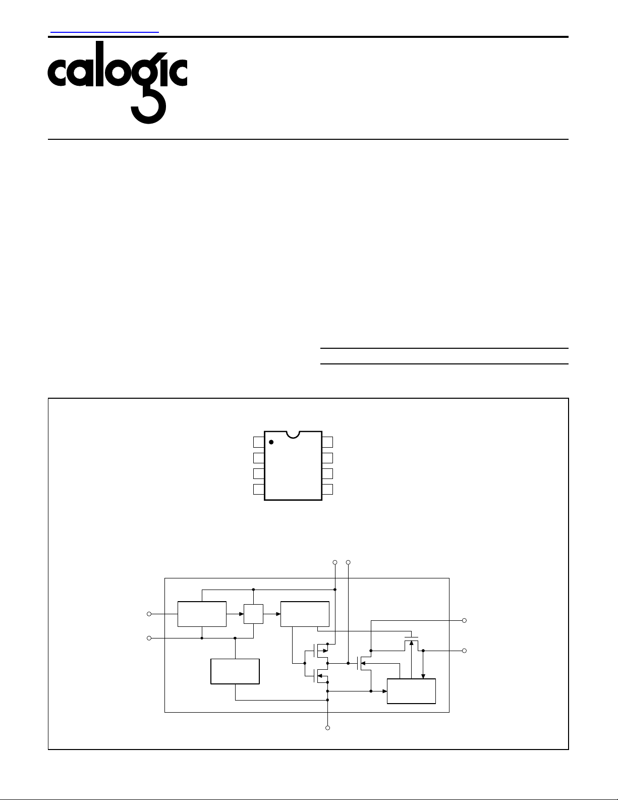
PIN CONFIGUR ATION AND BLOCK DIAG RAM
NC 1
+
CAP
2
GND
CAP
–
CLM7660
3
45
DESCRIPTION
Calogic CL M7660 DC-to-DC convert er will ge nerate a negative
voltage from a positive source. The CLM7660 generates -5V
in +5V digital systems and with tw o exter nal cap acitor s, the dev ice
will convert a 1.5V to 10V input signal to a -1.5V to -10V level.
Applications include analog-to-digital converters, digital-to-analog
converte rs, operat ional ampli fiers and mul tiplex ers. Many of these
systems require negative supply voltages. The CLM7660 allows
+5V digital logic systems to incorporate these analog com ponent s
without an additional main power source. Lower part count, less real
estate, ease of use ar e just a few of the benefi ts of the CLM7 660.
ORDERING INFORMATION
Part Package Temperature
o
CLM7660CP 8 Pin DIP -40
CLM7660DY 8 Pin SOIC -40
+
8
V
7
OSC
LOW
6
VOLTAGE (LV)
V
OUT
C to +85oC
o
C to +85oC
NC = NO INTERNAL CONNECTION
1K-17
+
+
CAP
V
2
8
OSC
7
6
LV
RC
OSCILLATOR
INTERNAL
VOLTAGE
REGULATOR
÷2
VOLTAGE-
LEVEL
TRANSLATOR
3
GND
LOGIC
NETWORK
4
5
CAP
V
OUT
1B-35
–
CALOG IC CORPOR ATION, 237 Whitney Place, Fremont, California 94539, Telephone: 510-656-2900, FAX: 510-651-3025
CLM7660
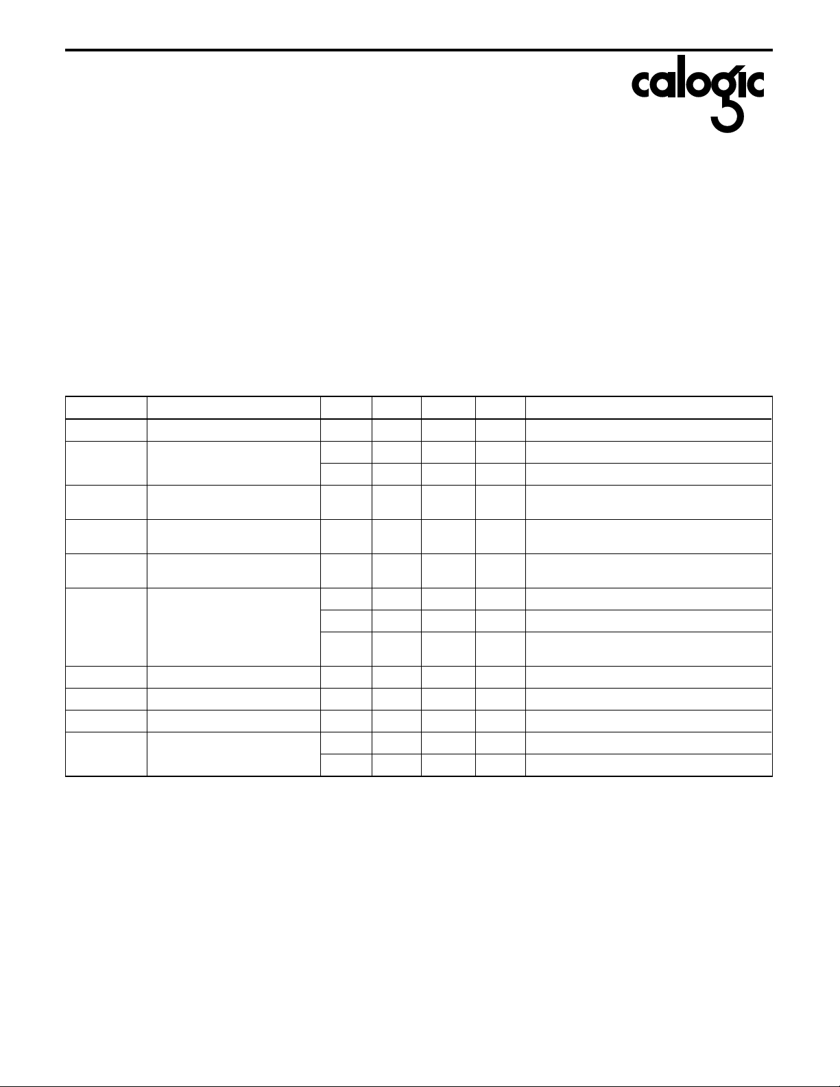
ABSOLUTE MAXIMUM RATINGS
Supply Voltage. . . . . . . . . . . . . . . . . . . . . . . . . . . . . . . +10.5V
L V and OSC I nput s
Volt age ( Not e 1). . . . . . . . . . . . . . . . . . . -0.3V to (V
+
-5.5V) to (V++0.3V)
(V
Current into LV (Note 1). . . . . . . . . . . . . . . 20µA for V
Output Shor t Duration (V
≤ 5.5V). . . . . . . . Continuous
SUPPLY
Power Dissipation (Note 2)
Plastic DIP . . . . . . . . . . . . . . . . . . . . . . . . . . . . . . . . 375mW
for V
for V
+
+0.3V)
+
<5.5V
+
<5.5V
+
>3.5V
CORPORATION
Operating Temper at ur e Ra nge
D Suffix. . . . . . . . . . . . . . . . . . . . . . . . . . . . . -40
Storage Temper at ure Ra nge. . . . . . . . . . . . . -65
o
C to +85oC
o
C to +150oC
Lead Temperature (Soldering, 10 sec) . . . . . . . . . . . . +300
Static - se n si t iv e de v ic e . Unu s ed dev ic e s mus t be sto r ed in co nd uctive material.
Protect devices from static discharge and static fields. Stresses above those
listed under "Absolute Maximum Ratings" may cause permanent damage to the
device. These are stress ratings only and functional operation of the device at
these or any other conditions above those indicated in the operation sections of
the specifications is not implied. Exposure to absolute maximum rating
conditions for extended periods may affect device reliability.
o
C
ELECTRICAL CHARACTERISTIC S V+ = 5V, TA = +25oC, C
= 0, Te st Circuit (Figur e 1), unle ss otherwise indicat ed.
OSC
SYMBOL PARAMETER MIN TYP MAX UNIT TEST CONDITIONS
+
I
+
V
H1
Supply Current - 80 180 µARL = ∞
Supply Voltage Range, High 3 - 6.5 V 0oC ≤ TA ≤ +70oC, RL = 10kΩ, LV Open
3 - 5 V -55oC ≤ TA ≤ +125oC, 10kΩ, LV Open
+
V
V
V
R
f
OSC
L1
+
H2
+
L2
OUT
Supply Voltage Range, Low
(D
Out of Circu it)
X
Supply Voltage Range, High
(D
In Circuit)
X
Supply Voltage Range, Low
(D
In Circuit)
X
1.5 - 3. 5 V M in ≤ T
3 - 10 V Min ≤ T
1.5 - 3.5 V Min ≤ T
Output Source Resistance - 55 100 Ω I
--120Ω I
--300Ω V
Oscillator Frequency - 10 - kHz
≤ Max, RL = 10kΩ, LV to GND
A
≤ Max, RL = 10kΩ, LV Open
A
≤ Max, RL = 10kΩ, LV to GND
A
= 20mA, TA = 25oC
OUT
= 20mA, 0oC ≤ TA ≤ +70oC (C Device)
OUT
+
= 2V, I
o
0
C ≤ TA ≤ +70oC
= 3mA, LV to GND
OUT
PEF Power Efficiency 95 98 - % RL = 5kΩ
V
OUT EF
Z
OSC
Voltage Conversion Efficiency 97 99.9 - % RL = ∞
Oscillator Impedance - 1 - MΩ V+ = 2V
-100- kΩ V+ = 5V
NOTES:
1. Connecting any input terminal to voltages greater than C+ or less than GND may cause destructive latch-up. It is recommended that no inputs
from sources operating from external supplies be applied prior to "power up" of the CLM7660.
2. Derate linearly above 50
o
C by 5.5mW/oC.
CALOG IC CORPOR ATION, 237 Whitney Place, Fremont, California 94539, T elephone: 510-656-2900, FAX: 510-651-3025

CORPORATION
CIRCUIT DESCRIPTION
CLM7660
The CLM7660 is an excellent voltage doubler, the device has
all the characteristic with the exception of two i nexpensive
10µF polarized electrolytic external capacitors. Figure 3
demonstrates t he most ef fect ive m eans of using the device as
a voltage doubler. Capacitor C
for the half cycle when switches S
Switches S
and S4 are open during this half cycle.) During
2
the second half of the operation, switches S
closed, with S
and S3 open, thereby shifting capacitor C
1
is charged to a voltage, V+,
1
and S3 are closed. (Note
1
and S4 are
2
negatively by V+ volts. Charge is then transferred from C1 to
, such that voltage on C2 is exactly V+, asumming ideal
C
2
switches and no load on C
The four switches in Figure 3 are MOS power switches, S
a P-Channel device, S
.
2
, S3 and S4 are N-Channel devices.
2
is
1
The major challenge with this approach while integrating the
switches, the substrates of S
and S4 must always remain
3
reversed-biased with respect to their sources, but not so
much as to degrade their ON-resistances. In addition, at
circuit start-up, and under short circuit conditions (V
OUT
=V+),
the output voltage must be sensed and the substrate bias
adjusted accordingly. Fail ure to accomplish this will result in
high power losses an d probab le device latch- u p .
The above problem is eliminated in the CLM7660 by a logic
network which senses the output voltage (V
the level translators, and switches t h e substrates of S
) together with
OUT
and S
3
to the correct le vel to ma inta in neces sar y rever se bias.
The voltage regulator portion of the CLM7660 is an integral
part of the anti-latch-up circuitr y. Its inherent voltage d ro p ca n
degrade operation at low voltages. To improve low-voltage
operation, the LV pin should be connected to GND, disabling
the regulator. For supply voltages greater than 3.5V, the LV
terminal must be left open to ensure latch-up proof operation
and prevent device damage.
When larger values of C
and C2 are used, the CLM7660
1
approaches the above conditions for negative voltage
multiplication.
Energy is lost only if the transfer of the charge
between capacitors if a change in voltage oc cur s. The energ y
lost is defin ed by:
E=1/2C
During the pump and transfer cycles V
voltages on C
1
(V12-V22)
1
1
and V2 are the
1
. If the impedances of C1 and C2 are high at
the pump frequency (see Fi gure 3), compared to the value of
R
, there will be a substantial difference i n voltages V1 and
L
. The most optimum selection would be to make C2 as
V
2
large as possible to eliminate output voltage ripple, and to
utilize a large value for C
to achieve maximum efficiency of
1
operation.
OPERATIONAL RULES:
Never exceed maxim um supp ly voltages.
Never connect LV terminal to GND for supply voltages over
3.5V.
Never short circuit the output to V
+
supply voltages above
5.5V for extended periods; however, transient conditions
including start-up are accept ab le.
For polarized capacitors, the + terminal of C
4
connected to pin 2 of the CLM7660 and the + ter minal t o o f C
must be connected to GND.
For high-voltage, elevated temperature applications add a
diode D
(reference Figure 1). The 1N914 diode is an
X
appropriate choice.
must be
1
2
THEORETICAL PO WER E FF ICI ENCY CONSIDERATIONS
In theory, a voltage multiplier can approach 100% efficiency if
certain conditions are met :
1. The drive circuitr y consum es minim al power.
2. The output switches have extremely low ON-resistance and
virtually no of f set .
3. The impedances of the pump and reservoir capacitor s are
negligible at the pump frequency.
CALOG IC CORPOR ATION, 237 Whitney Place, Fremont, California 94539, T elephone: 510-656-2900, FAX: 510-651-3025

CLM7660
CORPORATION
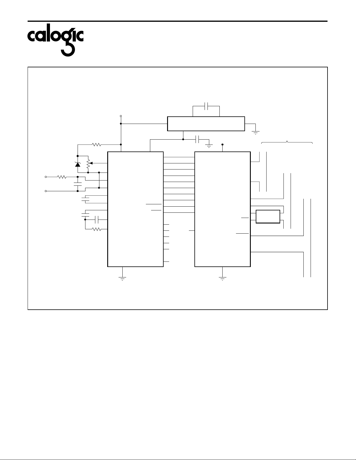
FIGURE 1. CLM7660 TEST CIRCUIT
1
2
+
C
1
10µF
1K-11
NOTES:
* For large values of C
values of C
** DX is required for supply voltages greater than 6.5V at
o
-55
≤ TA ≤ +70oC. Refer to performance curves for
additional information.
CLM7660
3
45
and C2 should be increased to 100µF.
1
8
7
6
(>1000pf), the
OSC
D**
X
C*
OSC
C
2
10µF
+
FIGURE 3. IDEALIZED SWITCHED CAP ACI TOR
+
V
GND
S
1
S
3
S
2
C
1
C
S
2
4
V
OUT
I
I
L
R
= –V
FIGURE 2. CHIP TOPOGRAPHY
S
+
V
(+5)
L
GND
C+
C-
V
OUT
LV
V
O
OSC
DIE SIZE = 81.5 x 57.5 (mm)
V8
1L-05
FIGURE 4. SIMPLE NEGATIVE CONVERTER
+
V
D
X
*
V
OUT
C
2
10µF
+
1K-12
1
2
+
C
1
10µF
IN
1K-05
*NOTES:
1. V
= -n V+ for 1.5V ≤ V+ ≤ 6.5V.
OUT
2. V
= -n (V+ –V
OUT
CLM7660
3
45
) for 6.5V ≤ V+ ≤ 10V.
FDX
8
7
6
FIGURE 5. P ARALLELI NG DEVI CES L OWERS OUTPUT IMPEDANCE
+
V
1
2
C
1
1K-06
CLM7660
3
45
"1"
8
7
6
C
1
D
X
1
2
CLM7660
3
45
"n"
8
7
D
6
X
+
R
L
C
2
CALOG IC CORPOR ATION, 237 Whitney Place, Fremont, California 94539, T elephone: 510-656-2900, FAX: 510-651-3025

CORPORATION
X
D
+
1J-49
1
2
3
8
7
6
4
5
CLM7660
+
2
D
3
C
+
V
+
4
C
2
C
+
+
1
C
OUT
V
OUT
V
(2V
) – (2V
F
)
=
1
D
V
F
= –(V+–
)
FIGURE 6. INCREASED OUTPUT VO LTAGE BY CASCADING DEVICES
+
V
CLM7660
1
2
10µF
+
*NOTES:
1. V
= -n V+ for 1.5V ≤ V+ ≤ 6.5V.
OUT
2. V
= -n (V+ –V
OUT
CLM7660
3
45
"1"
) for 6.5V ≤ V+ ≤ 10V.
FDX
FIGURE 7. EXTERNAL CLOCKING
10µF
1K-08
1
2
+
CLM7660
3
45
8
7
6
8
7
6
+
10µF
D
X
1
2
CLM7660
3
45
"n"
8
7
D
6
X
+
V*
10µF
OUT
1K-07
FIGURE 8. LOWERING OSCILLA TO R FREQUENCY
+
V
1kΩ
D
X
+
V
1
CMOS
GATE
V
OUT
10µF
+
+
C
1
1K-09
2
CLM7660
3
45
8
7
D
6
X
+
V
C
OSC
V
OUT
C
2
+
FIGURE 9. POSITIVE VOLTAG E MU LTIPLIER
FIGURE 10. COMBINED NEGATIVE CONVERTER
AND POSITIVE MULTIPLI ER
+
V
1
2
CLM7660
3
45
8
7
6
D
1
+
D
2
C
1
V
OUT
(2V+) - (2VF)
+
C
2
=
1K-10
CALOG IC CORPOR ATION, 237 Whitney Place, Fremont, California 94539, T elephone: 510-656-2900, FAX: 510-651-3025

CLM7660
+
V
1K-02
31
30
32
35
36
LCD
DRIVE
(–5V)
1
10mF
CLM7660
2
4
5
3
+
26
10mF
+
IN
V
+
V
IN LO
IN HI
COM
REF LO
REF IN
CLM7106
3-1/2 DIGIT
A-D
+5V
CA1004
8
CORPORATION
FIGURE 11. POSITIVE VOLTAG E CONVERSION
OUT
1M
Ω
–
–
V INPUT
10µF
V = –V
1
2
+
C
1
1J-50
CLM7660
3
45
8
7
6
FIGURE 12. SPLITTING A SUPPLY IN HALF
+
50µF
50µF
50µF
1
2
CLM7660
3
45
100kΩ100kΩ
+
8
7
1MΩ
6
R
L1
V=
OUT
+V–
– V
2
R
L2
+
+
1K-01
10µF
FIGURE 13A. FIXED POWER SUPPLY OPERA TION
OF CLM7106 A- D
+
V
–
V
FIGURE 13B. NEGA TI VE POWER SUPPLY GENERATION FOR 3 1/2 DIGIT A-D
+
CLM7660
42
8
35
+
COMMON ANODE
LED DISPLAY
26
LED
DRIVE
–
V
CLM7107A
3-1/2 DIGIT
A-D
21
+5V
V
GND
1
+
REF IN
REF LO
IN LO
COM
IN HI
36
35
32
31
V
30
IN
1K-03
CALOG IC CORPOR ATION, 237 Whitney Place, Fremont, California 94539, T elephone: 510-656-2900, FAX: 510-651-3025
CORPORATION
FIGURE 14. CLM7660 SUPPLIES -5V FOR CO NVERTERS IN MICRO PRO CESSO R-CO NTRO LLED
DATA ACQ UI SIT ION SYSTEMS
µ
F
10
+
+
ANALOG
INPUT
–
1K-04
CA1004
100k
0.1
+5V
CLM7660
5
2
3
4
5
6
7
8
9
40
39
10
µ
F
PA0
PA1
PA2
PA3
PA4
PA5
PA6
PA7
CA1
CA2
PB0-PB7
+
Ω
20k
+
2
REF IN
3
ANALOG
COMMON
+ INPUT
9
– INPUT
7
REF CAP
8
REF CAP
4
INT OUT
5
AZ IN
6
BUFF OUT
V
DIGITAL
GND
–
+
A-D=7135
100k
Ω
Ω
µ
F
1µF
0.47
µ
F
1
100k
10
µ
F
Ω
–5V
–
V
OR
UR
POL
STROBE
RUN/HOLD
BUSY
CLOCK IN
B1
B2
B4
B8
D5
D1
D2
D3
D4
13
14
15
16
27
28
23
12
26
25
20
NC
19
NC
18
NC
17
NC
21
NC
CLOCK
22
INPUT
f = 120kHz
42
38
+5V
RS0
RS3
CS1
CS2
RESET
R/W
IRQ
D0
D7
O2
.
.
.
.
.
.
.
.
DATA BUS
20111
SY65224-1/2 DIGIT
V
SS
124
ADDRESS
DECODER
CLM7660
6502 µP BUS
ADDRESS
BUS
CONTROL
BUS
CALOG IC CORPOR ATION, 237 Whitney Place, Fremont, California 94539, T elephone: 510-656-2900, FAX: 510-651-3025

CLM7660
PERFORMANCE CURVES
vs OUTPUT CURRENT
CORPORATION
OUTPUT VOLTAGE
0V
2V
–1V
–2V
–3V
5V
–4V
–5V
–6V
OUTPUT VOLTAGE
–7V
–8V
10V
–9V
–10V
10
20 30 40 50 60 70
OUTPUT CURRENT (mA)
200Ω
100%
90%
300µA
200µA
100µA
1K-13
OUTPUT RESISTANCE
vs SUPPLY VOLTAGE
@ 5V EFFICIENCY vs
OSCILLATOR FREQUENCY (5mA)
95
@ 5V POWER CONSUMPTION vs
OSCILLATOR FREQUENCY (NO LOAD)
7.4
92
12.6
15 10
OSCILLATOR FREQUENCY (kHz)
1K-14
100Ω
OUTPUT RESISTANCE
10V5V0
INPUT VOLTAGE
1K-15
CALOGIC CORPOR ATION, 237 Whit ney Place, Fremont, California 9453 9, Tele phone: 510-656-290 0, FAX: 510-651-3025
 Loading...