

查询CLM4122供应商
CORPORATION
4mW, 180MHz, 2000V/µs
High Speed Buffer
CLM4122 / CLM4322
FEATURES
High Slew Rat e. . . . . . . . . . . . . . . . . . . . . . . . . . 2000V/µs
••
Wide Ban dw idt h. . . . . . . . . . . . . . . . . . . . . . . . . . 180MHz
••
Low Supply Current . . . . . . . . . . . . . . . . . . . . . . . 800µA
••
No Oscillations w it h Capacitive Lo ads
••
Fully S p e ci fi e d to Drive 50Ω Lines
••
APPLICATIONS
Coaxial Cable Driver
••
Flash A/D Converter Driver
••
Video DAC Buffer
••
Video Am pl ifier
••
Wide Ban dwi dt h Signal Condi t ioni ng
••
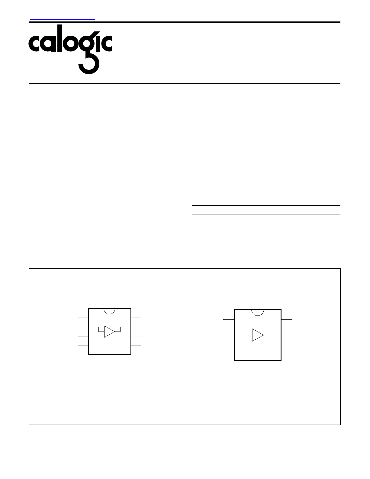
CONNECTION DIAGRAMS
GENERAL DESCRIPTION
The CLM4122 family are low power, high speed unity gain
buffers that slew at 2000V/µs, having a small signal
bandwidth of 180MHz, delivers 60mA, yet draws only 800µA
supply current .
The 4mW power consumpt ion, fast slew rate, w ide bandwidth,
and high output drive make the CLM4122 family the ideal
choic e fo r battery operated eq u ip m en t .
These same characteristics are the excellent choices for
driving coaxial and switched pair ca bles.
ORDERING INFORMATION
Part Package Temperature Range
o
CLM4122 N NO8A (Plas tic P Dip 8 Lead) -40
CLM41 22 M MO8B (SO I C 8 Le a d) -40
CLM4322 N NO8A (Plas tic P Dip 8 Lead) -25
CLM43 22 M MO8B (SO I C 8 Le a d) -25
C to 85oC
o
C to 85oC
o
C to 70oC
o
C to 70oC
Plastic DIP
1
*V-
2
V
IN
3
N/C
45
*V-
*Heat-sinking pins. Pin 1 and Pin 8
must be connected to the negative supply.
Package NO8A Package MO8B
CALOGIC CORPORATION, 237 Whitney P lac e, Fremont, C alifornia 9453 9, Telephone: 5 10-656-2900, FAX: 510-651- 10 76
8
V-*
7
V
OUT
6
V+
V-*
*V- V-*
V
IN OUT
N/C
*V- V-*
*Heat-sinking pins. Pin 1 and Pin 8
must be connected to the negative supply.
Plastic SO
1
2
3
45
8
7
V
6
V+
CLM4122 / CLM4322
ABSOLUTE MAXIMUM RATINGS (Note 1)
Supply Voltage. . . . . . . . . . . . . . . . . . . . . . . . . . . . . . . . . . +10
Input Voltage . . . . . . . . . . . . . . . . . . . . . . . . . . . . . . ±Vsupply
Storage Temperature Ra nge. . . . . . . . . . . . -65
Lead Temper at ur e
(Soldering 10 seconds) . . . . . . . . . . . . . . . . . . . . . . 260
Power Dissipation . . . . . . . . . . . . . . . . . . . . . . . . . . . (Note 4)
DC ELECTRICAL CHARACTERISTICS
The following specifications apply for Supply Vo ltag e = +5V, V
Boldface limits apply for T
= TJ = T
A
SYMBOL CHARACTERISTICS TYP
A
A
V
I
C
R
I
V
V
I
V1
V2
OS
B
IN
O
S
O1
O2
OUT
Voltage Gain 1 0.970 0.950 0.950
Voltage Gain 2 0.900 0.800 0.800 RL = 50Ω, VIN = +3V
Offset Voltage 5 25 40 mV Max VIN = 2. 5V
Input Bias Current 1 6 10 µA Max RL = 1KΩ, RS = 10kΩ,
Input Capacitance 3.5 pF
Output Resistance 3
Supply Current 825 1100 1200 µA Max RL = ∞
Output Swing 1 4.5 4 4
Output Swing 2 3.5 3.0 3.0 RL = 100Ω
Output Current 60 44 44 mA VIN = +4V
MIN
to T
o
C to +150oC
o
; all other limits TA = TJ = 25oC.
MAX
CLM4122 CLM4322
Limit
(Note 5)
5
10
CORPORATION
ESD Tolerance (Note 3). . . . . . . . . . . . . . . . . . . . . . . ±2000V
Therma l Re sistance (θ
) (Note 6)
JA
N Package . . . . . . . . . . . . . . . . . . . . . . . . . . . . . . . 50
M Package . . . . . . . . . . . . . . . . . . . . . . . . . . . . . . . 60
C
Maximum J unction Temperature . . . . . . . . . . . . . . . . . . 150
= 0, RL ≥ 100KΩ and RS = 50Ω unless otherwise noted.
CM
Limit
(Note 5)
5
6
UNITS CONDITIONS
V/V Min
Ω Max I
V
RL = 1KΩ, VIN = +3V
= 0 to 1mA
OUT
RL = 1K
o
C/W
o
C/W
o
C
AC ELECTRICAL CHARACTERISTICS
The following specifications apply for Supply Vo ltag e = +5V, R
Boldface limits apply for T
= TJ = T
A
SYMBOL CHARACTERISTICS TYP
SR
SR
SS
LS
P
t
r
t
pd
O
BW
, t
S
1
2
BW
BW
f
Slew Rate 1 2000 1500 1200
Slew Rate 2 1000 700 600 RL = 50Ω (Note 2)), V
Small Signal Bandwidth 180 140 100
Large Signal Bandwidth 170 130 100 VIN = +4V, RL = 1K, CL ≤ 10pF
Power Bandwidth 100 70 60 VIN = +4V, RL = 50Ω, CL ≤ 10pF
Rise Time Fall Time 2.0 2.5 3.5 ns RL = 50Ω, CL ≤ 10pF, VO = 100mV
Propagation Delay Time 3.0 ns RL = 50Ω, CL ≤ 10pF, VO = 100mV
Overshoot 10 % RL = 50Ω, CL ≤ 10pF, VO = 100mV
Note 1: Absolute Maximu m Rating s indicate limits beyond which dama ge to the device may occur. DC and AC electrical specification s do no t
apply when operating the device beyond its rated operati ng conditi on s.
Note 2: Slew rate is measured with 50Ω source impedance at 25
should be at least 5000V/µs.
Note 3: The test circuit consists of the human body model of 120pF in series with 1500Ω.
Note 4: The maximum power dissipation is a function of T
temperature is P
D
= (T
J(max)
- TA)/θJA.
Note 5: Limits are guaranteed by testing, correlation or periodic characterization.
Note 6: For M & N package, θ
is measured by soldering the unit directly on a printed circuit board and V- pins are connected to 2 square
JA
inches of 2 oz copper.
MIN
to T
; all other limits TA = TJ = 25oC.
MAX
CLM4122 CLM4322
Limit (Note 5) Limit (Note 5)
J(max), θJA
≥ 100KΩ and RS = 50Ω unless otherwise no ted.
L
UNITS CONDITIONS
V/µs
RL = 1KΩ (Note 2), V
IN
IN
= 3.5V
= 3.5V
PP
PP
VIN = 10 0mVPP, RL = 50Ω, CL ≤ 10pF
MHz
PP
PP
PP
o
C with input DC offset to 2.5V. For accurate measurements, the input slew rate
and TA. The maximum allowable power dissipation at any ambient
CALOGIC CORPORATION, 237 Whitney P lac e, Fremont, C alifornia 9453 9, Telephone: 5 10-656-2900, FAX: 510-651- 10 76

CORPORATION
TYPICAL PERFORMANCE CHARACTERI STI CS
CLM4122 / CLM4322
GAIN (dB)
-3dB BANDWIDTH (MHz)
0
-2
-4
-6
-8
190
180
170
160
150
140
130
120
110
100
FREQUENCY RESPONSE
RL= 1K
V
≤ 100mV
IN
C
≤ 10pF
L
T
= 25˚C
j
11025
20 50 400100 200
FREQUENCY (MHz)
SUPPLY VOLTAGE
vs BANDWIDTH
RL= 1K
642
SUPPLY VOLTAGE (VOLTS)
RL= 50Ω
8
80
64
48
32
16
0
FREQUENCY RESPONSE
PHASE LAG (DEGREES)
GAIN (dB)
0
-2
-4
-6
-8
RL= 50Ω
V
≤ 100mV
IN
C
≤ 10pF
L
T
= 25˚C
j
11025
FREQUENCY (MHz)
20 50 400100 200
80
60
40
20
0
PHASE LAG (DEGREES)
INPUT VOLTAGE
vs SLEW RATE
R
= 1KΩ
L
RL= 50Ω
12345
(V )
V
IN
P-P
s) (THOUSANDS)
µ
SLEW RATE (V/
2600
2400
2200
2000
1800
1600
1400
1200
1000
800
600
400
200
0
BANDWIDTH
RL= 1K
RL= 50Ω
406080
20
FREQUENCY (MHz)
100
120
140
160
180
200
1700
1600
1500
1400
A)
1300
µ
1200
1100
1000
900
800
700
600
500
400
SUPPLY CURRENT (
300
200
100
0
13579
SUPPLY VOLTAGE
vs SUPPLY CURRENT
SUPPLY VOLTAGE (VOLTS)
(p-p)
OUT
V
(LARGE SIGNAL & POWER)
5.5
5
4.5
4
3.5
3
2.5
2
1.5
1
0
CALOGIC CORPORATION, 237 Whitney P lac e, Fremont, C alifornia 9453 9, Telephone: 5 10-656-2900, FAX: 510-651- 10 76

CORPORATION
MO8B DIMENSION S
12
.050
(1.27)
5678
34
.020
.013
.213
.205
(5.4)
(5.2)
(TOP VIEW)
MO8B-8 LEAD SOIC
(.50)
(.33)
NO8A DIMENSIONS
0.150
(3.81)
MIN
0.023
0.014
.210
.205
(5.32)
(5.19)
.010
.004
0.005
(1.13)
MAX
0.405 MAX
(10.29)
(0.58)
(0.36)
.074
.070
(1.87)
(1.77)
(.25)
(.10)
0.06
0.15
(1.52)
(0.38)
0.070
0.030
8-Pin Plastic Dip
0.055
(1.40)
MAX
0.200
(5.08)
MAX
0.200
(5.08)
0.125
(3.18)
(1.78)
(0.76)
.318
.302
(8.10)
(7.64)
.023
(.58)
.019
(.48)
0.320
(8.13)
0.290
(7.37)
0.310
(7.87)
0.220
(5.59)
0.015
o
15 MAX
0.290
All Dimensions in
inches and
(millimeters)
.010
.006
(.25)
(.15)
(0.38)
(0.20)
Inform at ion furni shed by Calogic is believed to be accurate and reliable. Howe ver, no responsibility is assum ed for its use: nor for any in fring eme nt of pate nts or other
rights of third parties which may result from its use. No license is granted by implication or otherwise under any patent rights of Calogic.
CALOGIC CORPORATION, 237 Whitney P lac e, Fremont, C alifornia 9453 9, Telephone: 5 10-656-2900, FAX: 510-651- 10 76
 Loading...