

FA7615CP(E)
1
■ Description
The FA7615CP(E) is a bipolar IC containing basic circuit
necessary for PWM-type switching power supply control. This
IC can be operated by external synchronizing pulses.
■ Features
• External synchronization input terminal
• Low-voltage operation (V
CC = 3.6 to 22V)
• Totem-pole predriver
• Latch-mode short-circuit protection function (no malfunction
due to electrical noise)
• One capacitor shared for short-circuit protection and for softstart to minimize the number of external discrete components
■ Applications
• Battery power supply for portable equipment
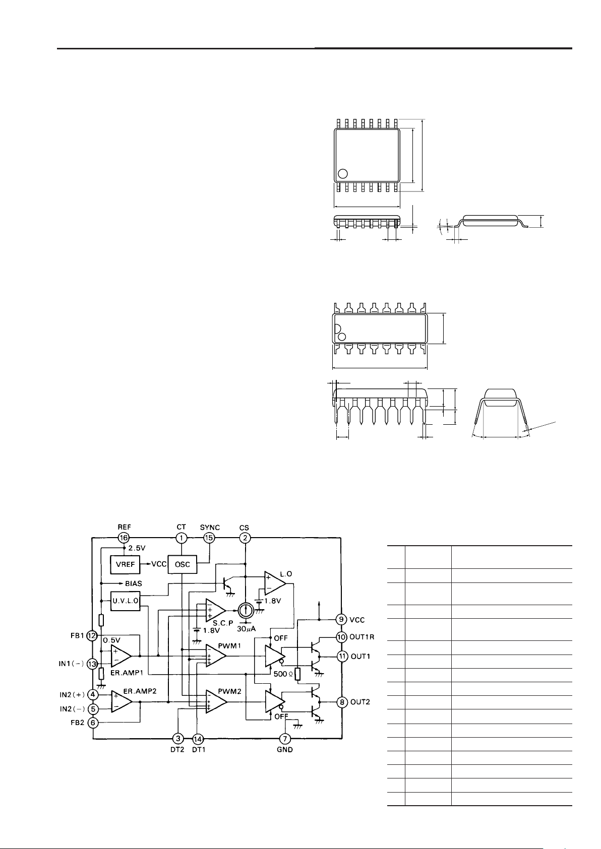
■ Dimensions, mm
Á SSOP-16
1
8
9
16
0.6
0~10˚
0.65
7.9
±0.3
5.3
6.2
0.1
±0.1
0.2
+0.1
–0.05
0.3
2.1max
Á DIP-16
■ Block diagram
FA7615CP(E)
Bipolar IC
For Switching Power Supply Control
Pin Pin Description
No. symbol
1 CT Oscillator timing capacitor
2 CS
Capacitor for soft-start,
short-circuit protection and delay
3 DT2 Dead time adjustment
4 IN2 (+) Non-inverting input to error
amplifier
5 IN2 (–) Inverting input to error amplifier
6 FB2 Error amplifier output
7 GND Ground
8 OUT2 CH. 2 Output
9 VCC Power supply
10 OUT1R CH. 1 Current limiting resistor
11 OUT1 CH. 1 Output
12 FB1 Error amplifier output
13 IN1 (–) Inverting input to error amplifier
14 DT1 Dead time adjustment
15 SYNC External synchronization input
16 REF Reference voltage output (2.5V)
1
16
9
8
19.4
6.5
7.6
3.4
4.3max
1.5
0.81
3.1min
0.2min
0~15˚
0~15˚
0.5
±0.1
2.54
±0.25
0.3
+0.1
–0.05
FA7615CP(E)
2
■ Electrical characteristics (Ta = 25°C, VCC = 6V, RT = 47kΩ, CT = 1000pF)
Reference voltage section
Item Symbol Test condition Min. Typ. Max. Unit
Output voltage VREF IOR = 1mA 2.383 2.432 2.481 V
Line regulation LINE VCC = 3.6 to 20V, IOR = 1mA 4 12 mV
Load regulation LOAD IOR = 0.1 to 1mA 1 6 mV
Output voltage variation due to temperature change VTC1 Ta = –20 to +25°C–1 1%
VTC2 Ta = +25 to +85°C–1 1%
Oscillator section
Item Symbol Test condition Min. Typ. Max. Unit
Oscillation frequency fOSC CT = 1000pF, RT = 47kΩ 17 20 23 kHz
Frequency variation 1 (due to supply voltage change) fdV VCC = 3.6 to 20V 1 %
Frequency variation 2 (due to temperature change) fdT Ta = –20 to +85°C5%
Synchronizing terminal input current ISYNC VSYNC = 2V 0.4 1.0 mA
Synchronizing terminal input voltage VSYNC 1 2.5 V
Error amplifier section
Item Symbol Test condition Min. Typ. Max. Unit
Reference voltage VB 0.484 0.494 0.504 V
Input bias current IB 5 100 nA
Open-loop voltage gain AV 70 dB
Unity-gain bandwidth GB 1.0 MHz
Maximum output voltage (Pin 6 and Pin 12) VOM+ RNF = 100kΩ
V
REF
–0.2
V
VOM– RNF = 100kΩ 200 mV
Output source current (Pin 6 and Pin 12) IOM+ VOM = 1V 40 85 200
µ
A
PWM comparator section
Item Symbol Test condition Min. Typ. Max. Unit
Input threshold voltage (Pin 6 and Pin 12) VTH0 Duty cycle = 0% 0.38 0.48 V
Input threshold voltage (Pin 6 and Pin 12) VTH50 Duty cycle = 50% 0.6 V
■ Absolute maximum ratings
Item Symbol Rating Unit
Supply voltage VCC 22 V
Reference voltage output current
IOR 5mA
Output current IO ±50 mA
Total power dissipation Pd 400 mW
Operating temperature Topr –20 to +85 °C
Storage temperature Tstg –40 to +150 °C
■ Recommended operating conditions
Item Symbol Min. Max. Unit
Supply voltage VCC 3.6 20 V
Feedback resistance RNF 100 kΩ
Oscillator timing capacitor CT 220 22,000 pF
Oscillator timing resistance RT 10 100 kΩ
Oscillation frequency fOSC 5 200 kHz
 Loading...