

F A7610CP(N)/12CP(N)/17CP(N)
FA7610CP(N)/FA7612CP(N)/FA7617CP(N)
Bipolar IC
For Switching Power Supply Control
■ Description
The FA7610CP(N), 7612CP(N) and 7617CP(N) are bipolar
ICs containing basic circuits necessary for PWM-type
switching power supply control.
To minimize the number of external discrete components, the
FA7610CP(N) is provided for a flyback or step-up powersupply circuit, the FA7612CP(N) for a step-down power-supply
circuit and FA7617CP(N) for a flyback power supply circuit.
■ Features
FA7610CP(N)
• For flyback transformer-type or step-up power-supply circuit
(maximum output duty = 64% typical)
• Totem-pole predriver
• PWM-type switching power supply control
• Low-voltage operation (V
• Latch-mode short-circuit protection function (no malfunction
by noise)
• Soft-start function
• Undervoltage lockout function
• One capacitor shared for short circuit protection and for softstart to minimize the number of external discrete components
FA7612CP(N)
• For step-down power-supply circuit
(maximum output duty = up to 100%)
• Open collector output
• PWM-type switching power supply control
• Low-voltage operation (V
• Latch-mode short-circuit protection function (no malfunction
by noise)
• Soft-start function
• Undervoltage lockout function
• One capacitor shared for short circuit protection and for softstart to minimize the number of external discrete components
CC = 3.6 to 22V)
CC = 3.6 to 22V)
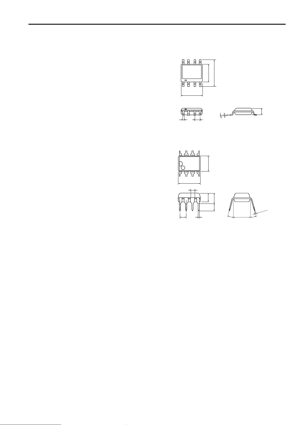
■ Dimensions, mm
Á SOP-8
4.9
1.27
5
4
±0.2
0.4
8
1
±0.1
Á DIP-8
±0.25
9.3
1.5
0.5
5
4
±0.1
8
1
2.54
3.9
6.5
3.4
±0.2
6.0
+0.1
0~8°
4.5max
3.0min
0~15˚
–0.05
0.20
7.6
0~15˚
0.3
+0.1
–0.05
1.7max
FA7617CP(N)
• For flyback transformer-type power-supply circuit (maximum
output duty = 67% typical)
• Open collector output
• PWM-type switching power supply control
• Low-voltage operation (V
CC = 3.6 to 22V)
• Latch-mode short-circuit protection function (no malfunction
by noise)
• Soft-start function
• Undervoltage lockout function
• One capacitor shared for short circuit protection and for softstart to minimize the number of external discrete components
■ Applications
• Battery power supply for portable equipment
1
FA7610CP(N)/FA7612CP(N)/FA7617CP(N)
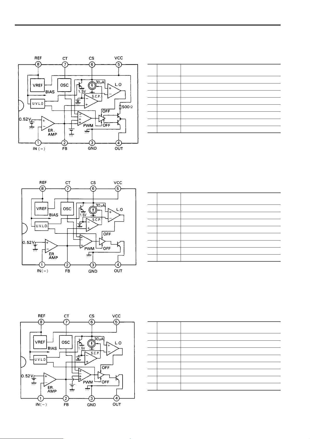
■ Block diagram
Á FA7610CP(N)
Pin Pin Description
No. symbol
1 IN (–) Inverting input to error amplifier
2 FB Error amplifier output
3 GND Ground
4 OUT Output
5 VCC Power supply
6 CS
7 CT Oscillator timing capacitor
8 REF Reference voltage output (2.5V)
Capacitor for soft-start, short-circuit protection and delay
Á FA7612CP(N)
Á FA7617CP(N)
Pin Pin Description
No. symbol
1 IN (–) Inverting input to error amplifier
2 FB Error amplifier output
3 GND Ground
4 OUT Output
5 VCC Power supply
6 CS
7 CT Oscillator timing capacitor
8 REF Reference voltage output (2.5V)
Capacitor for soft-start, short-circuit protection and delay
Pin Pin Description
No. symbol
1 IN (–) Inverting input to error amplifier
2 FB Error amplifier output
3 GND Ground
4 OUT Output
5 VCC Power supply
6 CS
7 CT Oscillator timing capacitor
8 REF Reference voltage output (2.5V)
Capacitor for soft-start, short-circuit protection and delay
2

FA7610CP(N)/FA7612CP(N)/FA7617CP(N)
■ Absolute maximum ratings (Ta = 25°C)
Item Symbol Rating Unit
FA7610C FA7612C/17C
Supply voltage VCC 22 22 V
Reference voltage output current IOR 55mA
Output current IO ±50 80 mA
Total power dissipation Pd 400 400 mW
Operating temperature Topr –20 to +85 –20 to +85 °C
Storage temperature Tstg –40 to +150 –40 to +150 °C
■ Recommended operating conditions
Item Symbol FA7610C FA7612/17C Unit
Min. Max. Min. Max.
Supply voltage VCC 3.6 20 3.6 20 V
Feedback resistance RNF 100 100 kΩ
Oscillator timing capacitor CT 220 22,000 220 22,000 pF
Oscillator timing resistance RT 10 100 10 100 kΩ
Oscillation frequency fOSC 5 200 5 500 kHz
■ Electrical characteristics (Ta = 25°C, VCC = 6V, RT = 33kΩ, CT = 1000pF)
Reference voltage section Common to FA7610C/12C/17C
Item Symbol Test condition Min. Typ. Max. Unit
Output voltage VREF IOR = 1mA 2.528 2.580 2.632 V
Line regulation LINE VCC = 3.6 to 20V, IOR = 1mA 4 12 mV
Load regulation LOAD IOR = 0.1 to 1mA 1 6 mV
Output voltage variation due to temperature change VTC1 Ta = –20 to +25°C–1 1%
VTC2 Ta = +25 to +85°C–1 1%
Oscillator section Common to FA7610C/12C/17C
Item Symbol Test condition Min. Typ. Max. Unit
Oscillation frequency fOSC CT = 1000pF, RT = 33kΩ 100 111 122 kHz
Frequency variation 1 (due to supply voltage change) fdV VCC = 3.6 to 20V 1 %
Frequency variation 2 (due to temperature change) fdT Ta = –20 to +85°C5%
Error amplifier section Common to FA7610C/12C/17C
Item Symbol Test condition Min. Typ. Max. Unit
Reference voltage VB 0.515 0.525 0.535 V
Input bias current IB 5 100 nA
Open-loop voltage gain AV 70 dB
Unity-gain bandwidth GB 0.6 MHz
Maximam output voltage (Pin 2) VOM+ RNF = 100kΩ
VOM– RNF = 100kΩ 200 mV
Output source current (Pin 2) IOM+ VOM = 1V 40 85 200
V
REF
–0.2
V
µ
A
PWM comparator section
Item Symbol Test condition FA7610C FA7612C FA7617C Unit
Min. Typ. Max. Min. Typ. Max. Min. Typ. Max.
Input threshold voltage (pin 2) VTH0 Duty cycle = 0% 0.85 0.95 0.85 0.95 0.85 0.95 V
Input threshold voltage (pin 2) VTH50 Duty cycle = 50% 1.1 1.1 1.1 V
Maximum duty cycle αM (Pin 2 = 1.2V) 58 64 75 100 63 67 71 %
3

FA7610CP(N)/FA7612CP(N)/FA7617CP(N)
Soft-start circuit section Common to FA7610C/12C/17C
Item Symbol Test condition Min. Typ. Max. Unit
Input bias current (Pin 6) IBCS 80 300 nA
Input threshold voltage (Pin 6) VTH CS0 Duty cycle = 0% 0.22 0.32 V
Input threshold voltage (Pin 6) VTH CS50 Duty cycle = 50% 0.46 V
Short-circuit protection circuit section Common to FA7610C/12C/17C
Item Symbol Test condition Min. Typ. Max. Unit
Input threshold voltage (Pin 2) VTH PC 1.20 1.50 1.80 V
Charge current (Pin 6) ICHG Pin 6 = 0V, Pin 2 = 2V 20 30 40
Latch-mode threshold voltage (Pin 6) VTH LA 1.20 1.50 1.80 V
Undervoltage lockout circuit section Common to FA7610C/12C/17C
Item Symbol Test condition Min. Typ. Max. Unit
OFF-to-ON threshold voltage VTH ON 2.70 V
ON-to-OFF threshold voltage VTH OFF 2.52 V
Voltage hysteresis VHYS 60 180 mV
Output section
µ
A
Item Symbol Test condition FA7610C FA7612C/17C Unit
Min. Typ. Max. Min. Typ. Max.
H-level output voltage (Pin 4) VOH RL = 10kΩ 3.54.0 ———V
L-level output voltage (Pin 4) VOL Output sink 0.25 0.65 0.9 1.5 V
Output source current (Pin 4) ISOURCE Pin 4 = 0V 8 11 14 ———mA
current = 20mA
Overall device
Item Symbol Test condition FA7610C FA7612C/17C Unit
Min. Typ. Max. Min. Typ. Max.
Supply current ICC LA Latch mode 1.6 2.2 1.5 2.2 mA
Operating-state supply current ICC AV RL = ∞ 2.6 3.8 1.8 3.0 mA
Duty cycle = 50%
4

FA7610CP(N)/FA7612CP(N)/FA7617CP(N)
■ Characteristic curves (Ta = 25°C)
Oscillation frequency(fOSC) vs. Output duty cycle vs. CS terminal voltage(VCS)
timing capacitor capacitance(C
Output source current (Isource) vs. L-level output voltage(VOL) vs. output sink current
supply voltage(V
CC)(ISINK)
T)
Supply current(ICC) vs. supply voltage(VCC) Error amplifier frequency(f) vs. voltage gain(AV) / phase (θ)
5

FA7610CP(N)/FA7612CP(N)/FA7617CP(N)
■ Application circuit
Á FA7610CP(N)
Flyback-transformer type converter circuit
Á FA7612CP(N)
Chopper type buck converter circuit
6

Á FA7617CP(N)
Flyback-transformer type converter circuit
FA7610CP(N)/FA7612CP(N)/FA7617CP(N)
VCC
0.52V
2.5V
0.01µ
VREF
U.V.L.O
36k
87
OSC.
+
ER.
AMP
12
0.01µ
330k
1000p
+
+
+
+
PWM
6
S.C.P
3
2.2k
180k
30µA
OFF
OFF
4.7µ
+
L.O
VCC
R2
+
3
R
5
TR
4
1k
Q1
+5V
+
–5V
+
Parts tolerances characteristics are not defined in the circuit design
sample shown above. When designing an actual circuit for a product,
you must determine parts tolerances and characteristics for safe and
economical operation.
Please connect a capacitor, which the value is about 0.01µF to 0.1µF,
between VCC and REF terminals in order to prevent from irregular
output pulse at start up.
18.75k
7
 Loading...