


California Micro Devices PRN299 Datasheet
CALIFORNIA MICRO DEVICES
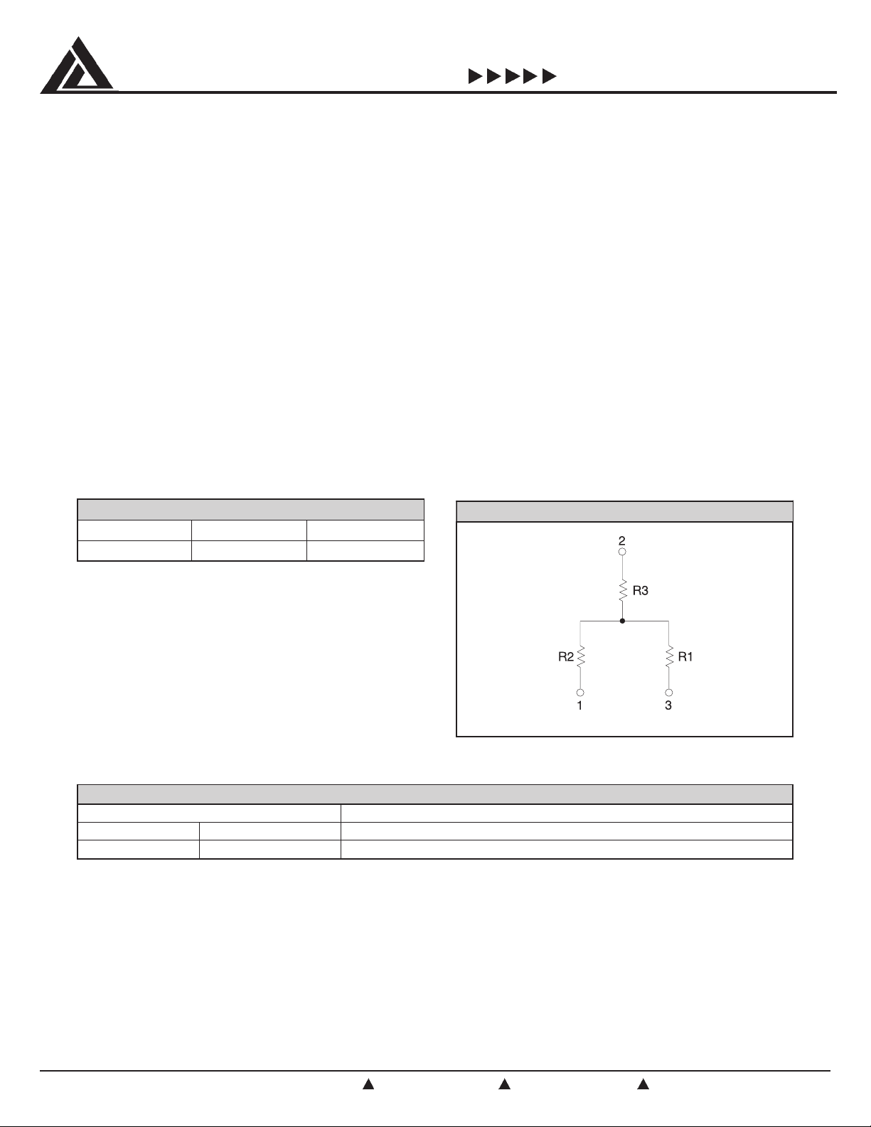
MARGAIDCITAMEHCS
PRN299
POSITIVE / PSEUDO ECL (PECL) CLOCK TERMINATION NETWORK
Features
Stable resistor network
Reduces power dissipation on the clock lines
Ideal for high-speed clock termination
Reduces board space by 70% vs. 1206 discretes
and component count by more than 50%
Applications
PECL clock termination
Application Note
High speed microprocessors line Intels Pentium/P6, Apple PowerPC, SPARC and other CISC and RISC based systems need
well-controlled and precise clock signals to maintain a synchronous systems. The fast edge rated clock signals will exhibit
transmission line effects on the clock lines resulting in undershoots and overshoots. The integrated PECL termination is
designed to suppress the undershoots and overshoots on the clock lines. The PECL RC terminator dissipates very low power
compared to the resistor termination network.
Why thin.film R networks? The PECL termination is an integrated R network fabricated on a silicon substrate using
advanced thin film technology. This will have a fixed time constant and will not create additional skew on the clock lines. It
has a low parasitic inductance compared to discrete and conventional thick film R terminators and provide effective termination
at high frequencies.
SEULAVDRADNATS
R
(
ΩΩ
ΩΩ
)
±%1R
Ω
1
05054.64
(
ΩΩ
ΩΩ
)
±%1R
Ω
2
(
ΩΩ
ΩΩ
)
±%1
Ω
3
TS
egakcaPrebmuNtraPgniredrO
sniPelytSgnikraMtraP
332-TOS992NRP
RADNA
When placing an order please specify desired shipping: Tubes or Tape & Reel.
© 2000 California Micro Devices Corp. All rights reserved.
3/00
215 Topaz Street, Milpitas, California 95035 Tel: (408) 263-3214 Fax: (408) 263-7846 www.calmicro.com
PAC VGA200 is a trademark of California Micro Devices Corp.
NOITAMROFNIGNIREDROTRAPD
1
CALIFORNIA MICRO DEVICES
SGNITARMUMIXAMETULOSBA
retemaraPgnitaRtinU
V,
V,
V
1CC
2CC
V&
3CC
4CC
:stupnitaegatlovCD V
2NI_CDD,1NI_CDDV,5.0-DNG
2NI_CNYS,1NI_CNYSV,5.0-DNG
:erutarepmeT
egarotS051+ot04-
tneibmAgnitarepO07+ot0
noitapissidrewopegakcaP0.1W
lobmySretemaraPsnoitidnoCNIMPYTXAMTINU
I
1CC
I
I
4CC
V
R
T
V
HI
V
LI
V
V
LO
R
b
R
c
I
N
3,2CC
SAIB
HO
R,
p
V
1CC
V
V,
2CC
3CC
V
4CC
V
SAIB
R
T
V
2CC
eulavrotsiseRV,PU_RWP
tnerructupnI
stupniOEDIVV
I
FFO
TEFNgnitfihsV(
V
NO
C
NI
t
HLP
t
LHP
t,
t
r
f
V
DSE
Note 1: These parameter applies only to the HSYNC and VSYNC channels.
Note 2: Per the IEC-61000-4-2 International ESD Standard, Level 4 contact discharge method. V
to GND via a low impedance ground plane with a 0.2uF, low inductance, chip ceramic capacitor at each supply pin. ESD pulse
is applied between the applicable pins and GND. ESD pulse can be positive or negative with respect to GND. Applicable pins
are: VIDEO_1, VIDEO_2, VIDEO_3, SYNC_OUT1, SD1, SYNC_OUT2, SD2, DDC_OUT1 and DDC_OUT2. All other pins are ESD
protected to the industry standard 2kV per the Human Body model (MIL-STD-883, Method 3015).
Note 3: This parameter is guaranteed by design and characterization.
©2000 California Micro Devices Corp. All rights reserved.
2
215 Topaz Street, Milpitas, California 95035 Tel: (408) 263-3214 Fax: (408) 263-7846 www.calmicro.com
egatlovylppus0.6+,5.0-DNGV
tnerrucdrawrof1DedoiD001Au
3_OEDIV,2_OEDIV,1_OEDIVV,5.0-DNG
5.0+V
1CC
3_MRET,2_MRET,1_MRET0.6+,0.6-V
5.0+
2CC
2TUO_CDD,1TUO_CDDV,5.0-DNG
tnerrucylppusV
tnerrucylppusV
tnerrucylppusV
1CC
V=
2CC
4CC
V
4CC
Vtanip
V
4CC
5.0+V
3CC
5.0+V
4CC
o
C
o
C
tastupniOEDIV;V5=V
V5=01Au
3CC
VtanipPU_RWP
;4CC
4CC
dedaolnustuptuo
egatlovtiucricnepoVmorfnwardtnerruclanretxeoN
ecnatsisernoitanimretOEDIV 52.175757.87
gnihctamecnatsiser 12%
1
egatlovtupnihgiHcigoL
1
egatlovtupniwoLcigoL
1
egatlovtuptuohgiHcigoL
1
egatlovtuptuowoLcigoL
rotsisernwod-llupV
stupniCNYSV,CNYSHV
levelssorcapordegatloVV
V
V
I
HO
I
LO
level,tnerrucegakaeletatsFFOV(
V0.5=0.2V
4CC
V0.5=8.0V
4CC
V,Am4-=
V,Am4=
3CC
V0.3=5.05.13MΩ
2CC
V;V5=
1CC
4CC
2CC
2CC
2CC
NI
V;V5=
NI
V-
)< V;V4.0
NI_CDD
V-
)< V;V4.0
TUO_CDD
V;V5.2=
V0.5=4.4V
4CC
V0.5=4.0V
4CC
V0.5=5.012MΩ
V=
V=
S
DNGro1±
1CC
DNGro1±
4CC
CDD_TUO
CDD_NI
I,DNG=
SD
NOdenrutnehwTEFNgnitfihs
3
ecnaticapactupnI
3_OEDIV,2_OEDIV,1_OEDIVV
3,2
egatlovdnatshtiwDSE
1CC
V
1CC
yalednoitagaporpH-LsrevirdCNYSC
L
yalednoitagaporpL-HsrevirdCNYSC
L
semitllaf&esirtuptuosrevirdCNYSC
L
V
1CC
V;V0.5=
NI
V;V5.2=
NI
V;Fp05=
CC
V;Fp05=
CC
V;Fp05=
CC
V=
V=
3CC
V5=8±Vk
4CC
PRN299
SCITSIRETCARAHCGNITAREPOLACIRTCELE
)esiwrehtodeificepssselnusnoitidnocgnitareporevo(
DNGro01Au
1CC
VroDNGtastupniCNYS;V5=
;01Au
4CC
dedaolnustuptuoCNYS
PU_RWP;V0.3tastupniCNYS;V5=002Au
dedaolnustuptuoCNYS;
CNYS;DNGtatupniPU_RWP;V5=01Au
nipV
SAIB
V=
2CC
V=
2CC
Am3=51.0V
zHM1taderusaem;V5.2=0.4Fp
zHM1taderusaem;V52.1=5.4
ttupnI;V5=
tdna
<sn5821sn
r
f
ttupnI;V5=
tdna
<sn5821sn
r
f
ttupnI;V5=
tdna
<sn57sn
r
f
, V
and V
CC1
CC3
8.0-V
4CC
Ω
µA
µA
01
µA
01
µA
must be bypassed
CC4
3/00