

California Micro Devices PACVGA201Q Datasheet
CALIFORNIA MICRO DEVICES
VGA PORT COMPANION CIRCUIT
PACVGA201
Features
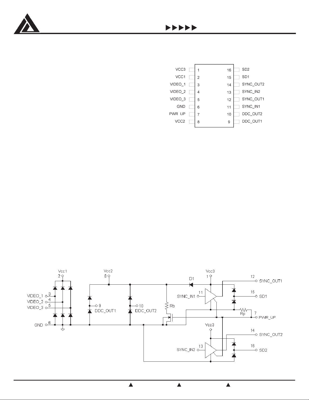
Pin Diagram
7 channels of ESD protection for all VGA port
connector pins meeting IEC-61000-4-2 Level-4 ESD
requirements (8KV contact discharge)
Very low loading capacitance from ESD protection
diodes on VIDEO lines, 4pF typical
TTL to CMOS level-translating buffers with power
down mode for HSYNC and VSYNC lines
Three power supplies for design flexibility
Compact 16-pin QSOP package
16-PIN QSOP PACKAGE
Product Description
The PACVGA201 incorporates 7 channels of ESD protection for all signal lines commonly found in a VGA port. ESD protection
is implemented with current steering diodes designed to safely handle the high surge currents encountered with IEC-61000-4-
2 Level-4 ESD Protection (8KV contact discharge). When a channel is subjected to an electrostatic discharge, the ESD current
pulse is diverted via the protection diodes into the positive supply rail or ground where it may be safely dissipated.
Separate positive supply rails are provided for the VIDEO, DDC_OUT and SYNC channels to facilitate interfacing with low
voltage video controller ICs and provide design flexibility in multiple-supply-voltage environments.
An internal diode (D1, in schematic below) is provided such that V
power supply input.) In applications where V
DDC_OUT pins back to the powered down V
may be powered down, diode D1 blocks any DC current path from the
CC3
rail via the upper ESD protection diodes.
CC3
is derived from V
CC2
CC3
. (V
does not require an external
CC2
Two non-inverting drivers provide buffering for the HSYNC and VSYNC signals from the Video Controller IC (SYNC1, SYNC2).
These buffers accept TTL input levels and convert them to CMOS output levels that swing between Ground and V
CC3
.
When the PWR_UP input is driven LOW the SYNC inputs can be floated without causing the SYNC buffers to draw any current
from the V
supply. When the PWR_UP input is LOW the SYNC outputs are driven LOW.
CC3
Schematic Diagram
© 2000 California Micro Devices Corp. All rights reserved.
4/00
215 Topaz Street, Milpitas, California 95035 Tel: (408) 263-3214 Fax: (408) 263-7846 www.calmicro.com
PAC VGA201 is a trademark of California Micro Devices Corp.
C0651299
1
CALIFORNIA MICRO DEVICES
PACVGA201
SGNITARMUMIXAMETULOSBA
retemaraPgnitaRtinU
V,
V
1CC
3CC
egatlovylppus0.6+,5.0-DNGV
:stupnitaegatlovCD V
3_OEDIV,2_OEDIV,1_OEDIVV,5.0-DNG
2TUO_CDD,1TUO_CDDV,5.0-DNG
2NI_CNYS,1NI_CNYSV,5.0-DNG
5.0+V
1CC
5.0+V
2CC
5.0+V
3CC
:erutarepmeT
o
egarotS051+ot04-
tneibmAgnitarepO07+ot0
C
o
C
noitapissidrewopegakcaP57.0W
SCITSIRETCARAHCGNITAREPOLACIRTCELE
)esiwrehtodeificepssselnusnoitidnocgnitareporevo(
lobmySretemaraPsnoitidnoCNIMPYTXAMTINU
I
1CC
I
3CC
V
V
HI
V
LI
V
HO
V
LO
R
b
I
N
C
NI
t
HLP
t
LHP
t
t,
r
V
V
1CC
V
3CC
V
2CC
R,
p
f
DSE
2CC
tnerrucylppusV
tnerrucylppusV
V
V
V5=01Au
1CC
VroDNGtastupniCNYS;V5=
3CC
VtanipPU_RWP
;3CC
3CC
Vtanip
3CC
3CC
;01Au
3CC
PU_RWP;V0.3tastupniCNYS;V5=002Au
dedaolnustuptuoCNYS;
CNYS;DNGtatupniPU_RWP;V5=01Au
dedaolnustuptuo
egatlovtiucricneponipV
2CC
Vmorfdeviredyllanretniegatlov
aivV
3CC
;nwardtnerruclanretxeon;1Dedoid
1
egatlovtupnihgiHcigoL
1
egatlovtupniwoLcigoL
2
egatlovtuptuohgiHcigoL
2
egatlovtuptuowoLcigoL
eulavrotsiseRV,PU_RWP
V
V
I
HO
I
LO
V0.5=0.2V
3CC
V0.5=8.0V
3CC
V,Am4-=
V,Am4=
3CC
V0.5=4.4V
3CC
V0.5=4.0V
3CC
V0.5=5.012MΩ
tnerructupnI
stupniOEDIVV
stupniCNYSV,CNYSHV
4
ecnaticapactupnI
1CC
3CC
3_OEDIV,2_OEDIV,1_OEDIVV
V
1CC
yalednoitagaporpH-LsrevirdCNYSC
L
yalednoitagaporpL-HsrevirdCNYSC
L
semitllaf&esirtuptuosrevirdCNYSC
4,3
egatlovdnatshtiwDSE
L
V
1CC
V;V5=
V=
NI
1CC
V;V5=
V=
NI
3CC
1CC
V;V0.5=
NI
V;V5.2=
NI
V;Fp05=
3CC
V;Fp05=
3CC
V;Fp05=
3CC
V=
V=
2CC
V5=8±Vk
3CC
DNGro1±
DNGro1±
ttupnI;V5=
tdna
r
ttupnI;V5=
r
ttupnI;V5=
r
<sn5821sn
f
tdna
<sn5821sn
f
tdna
<sn57sn
f
dedaolnustuptuoCNYS
8.0-V
3CC
zHM1taderusaem;V5.2=0.4Fp
zHM1taderusaem;V52.1=5.4
µA
µA
Note 1: These parameters apply only to SYNC_IN1, SYNC_IN2 and PWR_UP.
Note 2: These parameters apply only to SYNC_OUT1 and SYNC_OUT2.
Note 3: Per the IEC-61000-4-2 International ESD Standard, Level 4 contact discharge method. V
a low impedance ground plane with a 0.2uF or greater, low inductance, chip ceramic capacitor at each supply pin. ESD pulse is applied
between the applicable pins and GND. ESD pulse can be positive or negative with respect to GND. Applicable pins are: VIDEO_1,
VIDEO_2, VIDEO_3, SYNC_OUT1, SD1, SYNC_OUT2, SD2, DDC_OUT1 and DDC_OUT2. All other pins are ESD protected to the
industry standard 2kV per the Human Body model (MIL-STD-883, Method 3015).
Note 4: This parameter is guaranteed by design and characterization.
©2000 California Micro Devices Corp. All rights reserved.
2
215 Topaz Street, Milpitas, California 95035 Tel: (408) 263-3214 Fax: (408) 263-7846 www.calmicro.com
CC1
, V
CC2
and V
must be bypassed to GND via
CC3
4/00
 Loading...