

California Micro Devices PACDN017Q Datasheet
CALIFORNIA MICRO DEVICES
PAC DN017
18 CHANNEL ESD PROTECTION ARRAY WITH ZENER SUPPLY CLAMP
Features
18-channel ESD protection
Integral Zener diode clamp to suppress
supply rail transients
Applications
Parallel printer port protection
ESD protection for sensitive
electronic equipment.
15KV ESD protection (HBM)
15KV contact discharge ESD protection
per IEC 61000-4-2
Low loading capacitance, 7 pF typ.
24-pin QSOP package
Product Description
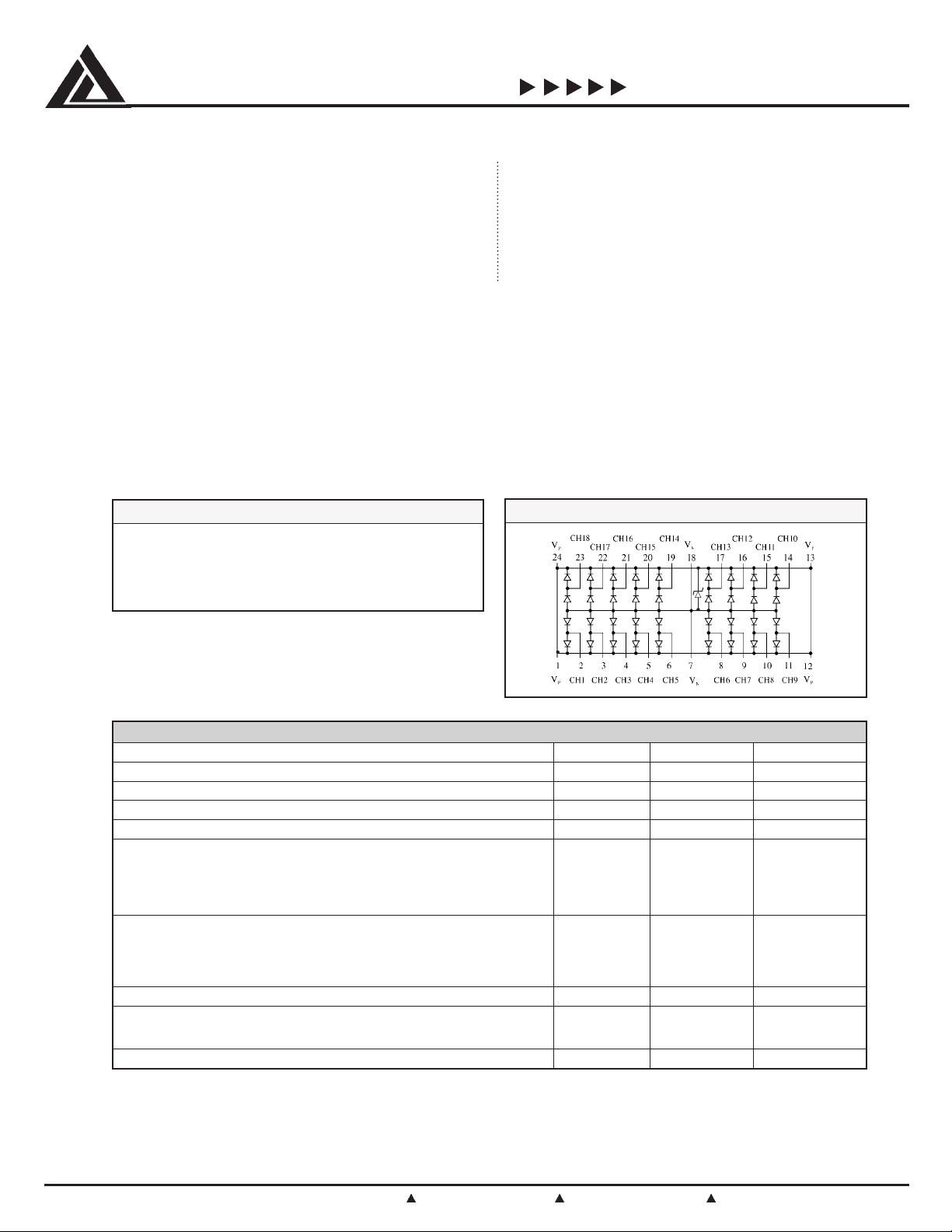
The PAC DN017 is a diode array designed to provide 18 channels of ESD protection for electronic components or
sub-systems. Each channel consists of a pair of diodes which steers the ESD current pulse either to the positive (V
negative (V
) supply. In addition, there is an integral Zener diode between VP and VN to supress any voltage
N
disturbance due to these ESD pulses. The PAC DN017 will protect against ESD pulses up to 15 KV Human Body
Model, and 15KV contact discharge per International Standard IEC 61000-4-2.
This device is particularly well-suited to provide additional ESD protection for parallel printer ports. It exhibits low
loading capacitance for all signal lines.
ABSOLUTE MAXIMUM RATINGS
Diode Forward DC Current
(Note 1) 40mA
Storage Temperature -65
°
C to 150°C
SCHEMATIC CONFIGURATION
Operating Temperature Range -20°C to 85°C
DC Voltage at any Channel Input V
-0.5V to VP+0.5V
N
P
) or
Note 1: Only one diode conducting at a time.
SNOITACIFICEPSDRADNATS
retemaraP.niM.pyT.xaM
V-
(egatloVylppuSgnitarepOV
V-
@tnerruCylppuSV
P
N
,egatloVdrawroFedoiDI
F
)V5.5
P
N
V5.5= Aµ02
C°52=T,Am02=V56.0V59.0
C°52=T,Am1@egatlovnwodkaerbesreverpmalcreneZ V6.6
noitcetorPDSE
)2etoN(
VK51±
VK51±
000 5103dohteM,ledoMydoBnamuH
000 2-4-00016CEIrepegrahcsiDtcatnoC
metsys-ni,tupnIlennahCynataegatloVegrahcsiDkaeP
)4,3etoN(
)5etoN(
C°52=T,MBHDSEVK51@egatloVpmalClennahC
)4,3setoN(
000stneisnartevitisoP
000stneisnartevitageN
V
P
V
N
V0.31-
C°52=T,tnerruCegakaeLlennahC Aµ1.0±Aµ0.1±
)zHM1@derusaeM(ecnaticapaCtupnIlennahC
V
P
Note 2: From I/O pins to VP or VN only. Bypass opacitor between VP and VN is not required. However, a 0.2 µF ceramic chip capacitor
Note 3: Human Body Model per MIL-STD-883, Method 3015, C
Note 4: This parameter is guaranteed by characterization.
Note 5: Standard IEC 61000-4-2 with C
V,V5=
bypassing V
,V0=VNIV5.2=
N
gnitaRrewoPegakcaP
to VN is recommended if the lowest possible channel clamp voltage is desired.
P
)4etoN(
Discharge
=150pF, and R
=100pF, R
Discharge
=330Ω, VP=5V, VN=GND.
Discharge
=1.5KΩ, VP=5.0V, VN=GND.
Discharge
Fp7Fp21
W0.1
V0.31+
©1999 California Micro Devices Corp. All rights reserved.
11/98
215 Topaz Street, Milpitas, California 95035 Tel: (408) 263-3214 Fax: (408) 263-7846 www.calmicro.com
P/Active® is a registered trademark and PAC is a trademark of California Micro Devices.
C0631199
1

CALIFORNIA MICRO DEVICES
Input Capacitance vs. Input Voltage
(pF)
IN
C
V
IN
Typical variation of CIN with V
(VP = 5V, V
= 0V, 0.1µF chip capacitor between V
N
PAC DN017
IN
& VN)
P
TS
RADNA
NOITAMROFNIGNIREDROTRAPD
egakcaPrebmuNtraPgniredrO
sniPelytSgnikraMtraP
42POSQQ710NDCAP
When placing an order please specify desired shipping: Tubes or Tape & Reel.
Application Information
See also California Micro Devices Application note AP209, Design Considerations for ESD protection.
In order to realize the maximum protection against ESD pulses, care must be taken in the PCB layout to minimize parasitic
series inductances to the Supply and Ground rails. Refer to Figure 1, which illustrates the case of a positive ESD pulse
applied between an input channel and Chassis Ground. The parasitic series inductance back to the power supply is
represented by L1. The voltage VZ on the line being protected is:
V
= Forward voltage drop of D1 + L1 x d(I
Z
where I
is the ESD current pulse, and V
esd
)/dt + V
esd
is the positive supply voltage.
Supply
Supply
Figure 1
An ESD current pulse can rise from zero to its peak value in a very short time. As an example, a level 4 contact discharge per
the IEC 61000-4-2 standard results in a current pulse that rises from zero to 30 Amps in 1nS. Here d(I
approximated by ∆I
© 1999 California Micro Devices Corp. All rights reserved.
2
215 Topaz Street, Milpitas, California 95035 Tel: (408) 263-3214 Fax: (408) 263-7846 www.calmicro.com
/∆t, or 30/(1x10
esd
-9
). So just 10nH of series inductance (L1) will lead to a 300V increment in VZ!
)/dt can be
esd
11/98
 Loading...