

California Micro Devices CSPDDR100 Datasheet
CALIFORNIA MICRO DEVICES
Chip Scale DDR Termination Array
CSPDDR100
Features
• 16 Integrated High frequency Series/Parallel
Terminations
• Ultra small footprint Chip Scale Package
• Ceramic substrate
• 0.35mm Eutectic Solder Bumps, 0.65mm Pitch
Product Description
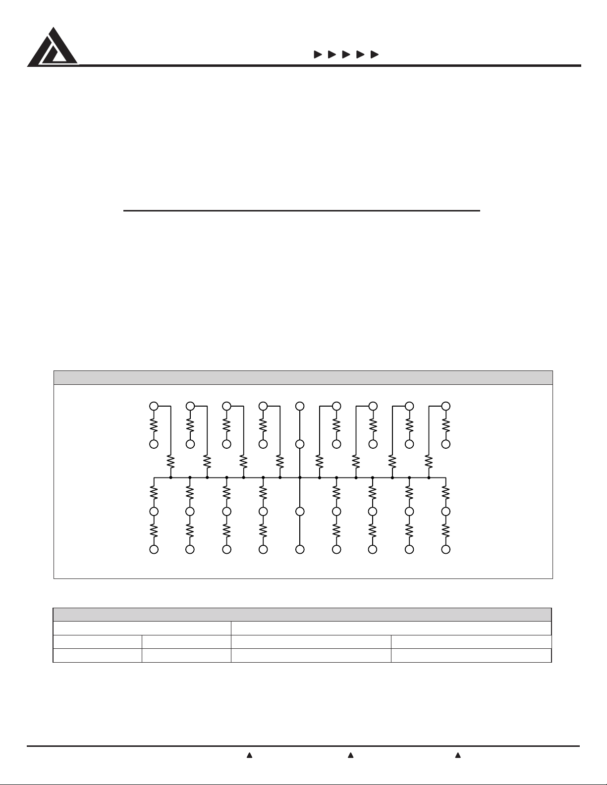
The CSPDDR100 is a high performance Integrated
Passive Device (IPD) which provides Series/Parallel
terminations suitable for use in SSTL and DDR termination applications. Sixteen (16) Series/Parallel termination
channels are provided for a total of 32 integrated
resistors. These resistors provide excellent high frequency performance in excess of 3GHz and are manufactured to an absolute tolerance of ±1%. The Chip
SCHEMATIC DIAGRAM
D
R1
R1
R1
R1
Applications
• DDR Memory bus termination
• SSTL Termination
Scale Package provides an ultra small footprint for
this Integrated Passive Device and provides minimal
parasitics compared to conventional packaging. Typical
bump inductance is less than 25pH. The large solder
bumps and ceramic substrate allow for standard attachment to laminate printed circuit boards without the use
of underfill. The 4X9 Bump pattern is arranged for easy
flow through routing on the pcb.
R1
R1
R1
R1
C
R2
R2
B
R1
A
12 34
R2
R1
R2
R2
R2
R1
R2
R1
R2
R2
5
R2
R2
R1
67 89
R2
R1
R2
R2
R2
R1
NOITAMROFNIGNIREDROTRAPDRADNATS
egakcaP rebmuNtraPgniredrO
elytSspmuBleeR&epaTgnikraMtraP
elacSpihC63001RDDPSC1ApmubkramottodknI
R2
R1
© 2000 California Micro Devices Corp. All rights reserved.
7/21/2000
215 Topaz Street, Milpitas, California 95035 Tel: (408) 263-3214 Fax: (408) 263-7846 www.calmicro.com
C1260700
1

CALIFORNIA MICRO DEVICES
Package Diagram (Bumps Up View)
0.65
0.297mm
D
mm
CSPDDR100
5.79mm
0.35mm
Dia.
Bumps
C
B
A
1
23456789
BCPnoeziSdaPmm003.0
epahSdaPdnuoR
noitinifeDdaP )DMSN(sdaPdenifeDksaMredloSnoN
gninepOksaMredloSmm053.0
ssenkcihTlicnetSredloSmm251.0
oitaRxulFredloS05/05
etsaPredloSnaelCoN
hsiniFecarTdnoB)A601sulPuCketnE(PSO
gninepOerutrepAlicnetSredloS).qs(mm063.0
0.65
mm
0.245
mm
2.44mm
0.381mm
0.875mm
SNOITADNEMMOCERDRAOBTIUCRICDETNIRP
Typical PCB Routing Diagram (Bumps Down View)
1
A
B
C
D
©2000 California Micro Devices Corp. All rights reserved.
2
9
7/21/2000215 Topaz Street, Milpitas, California 95035 Tel: (408) 263-3214 Fax: (408) 263-7846 www.calmicro.com
 Loading...