

California Micro Devices CMPWR130 Datasheet
CALIFORNIA MICRO DEVICES
T
S
ON
r
s
ubes
CMPWR130
300mA SmartORTM Regulator with V
Features
• Automatic detection of VCC input supply
• Glitch-free output during supply transitions
• Built-in hysteresis during supply selection
• 300mA output maximum load current
• Overload current protection
• Short circuit current protection
• Operates from either V
• 8-pin SOIC package
Product Description
The SmartORTM CMPWR130 is a low dropout regulator
that delivers up to 300mA of load current at a fixed 3.3V
output. An internal threshold level (TYP 4.1V) is used to
prevent the regulator from being operated below dropout
voltage. The device continuously monitors the input
supply and will automatically disable the regulator when
falls below the threshold level. When the regulator is
V
CC
disabled, the control signal “Drive” (Active Low) is
enabled, which allows an external PMOS switch to
power the load from an auxiliary 3.3V supply.
CC
or V
OUT
Drive
AUX
Applications
• PCI adapter cards
• Network Interface Cards (NIC’s)
• Dual power systems
• Systems with standby capabilities
When VCC is restored to a level above the select threshold, the control signal for the external PMOS switch is
disabled and the regulator is once again enabled.
All the necessary control circuitry needed to provide a
smooth and automatic transition between the supplies
has been incorporated. This allows V
switched without loss of output voltage.
to be dynamically
CC
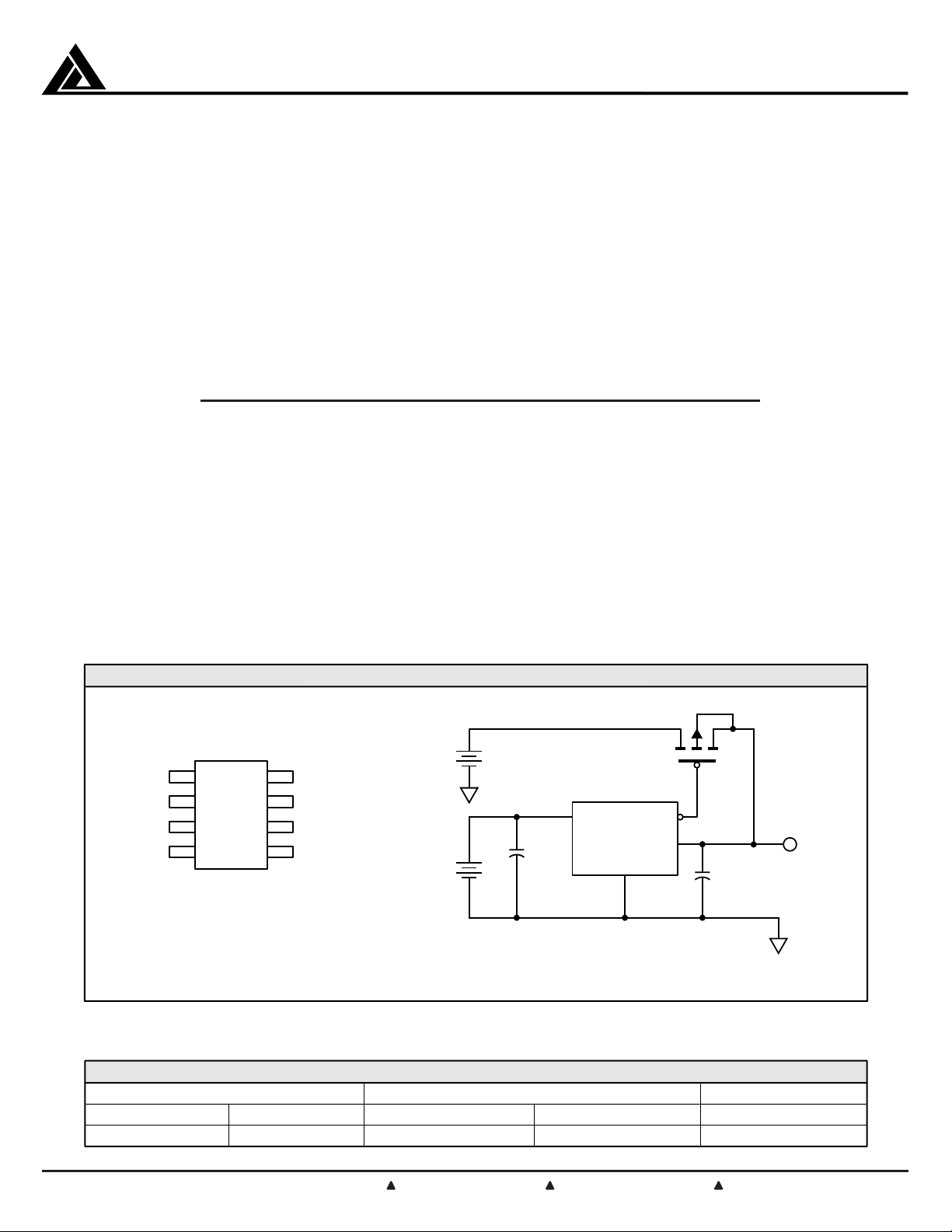
PIN DIAGRAM AND APPLICATION CIRCUI
Top View
81
CC
NC 72
NC 63
GND 5
4
CMPWR130
8-Pin SOIC
DRIVEV
V
V
NC
OUT
OUT
Pin Diagram
TANDARD PART ORDERING INFORMATI
Package Ordering Part Numbe
Pin
8 SOIC CMPWR130S/T CMPWR130S/R CMPWR130S
© 2001 California Micro Devices Corp. All rights reserved. SmartOR™ is a trademark of California Micro Devices Corp
215 Topaz Street, Milpitas, California 95035 Tel: (408) 263-3214 Fax: (408) 263-7846 www.calmicro.com
3/5/2001
Style T
MGSF1PO2ELT1
+
V
AUX
3.3V
–
GND
V
CC
+
5V
–
C
+
IN
1µF
CMPWR130
V
CC
DRIVE
GND
V
OUT
V
OUT
3.3V
300mA
+
C
OUT
4µF
GND
Typical Application Circuit
Tape & Reel Part Marking
C1670101
1
CALIFORNIA MICRO DEVICES
GS
g
Unit
)
000
O
S
Unit
CC
5 0.5
CS
)
C
UNIT
0
I
300
3.10
3.30
3.50
CMPWR130
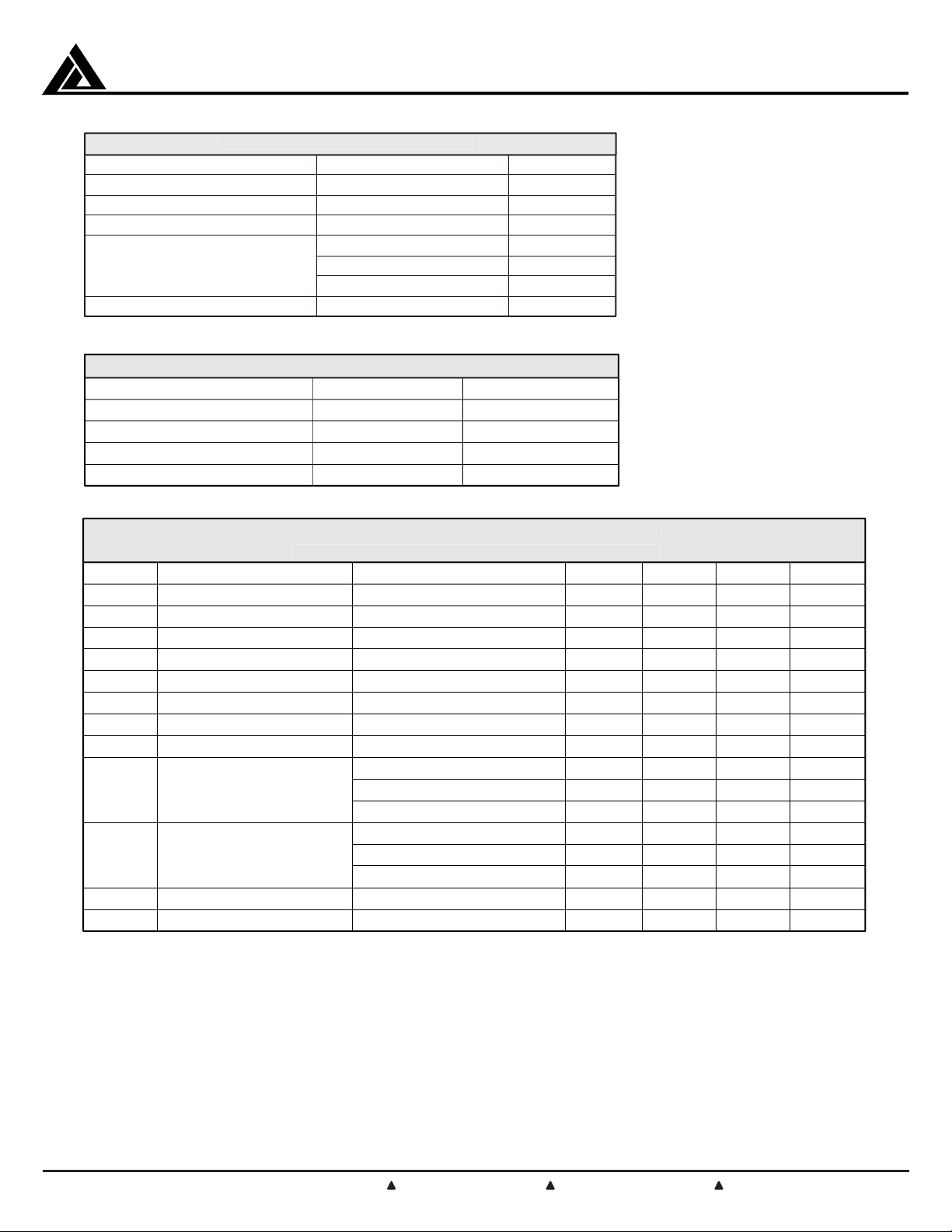
ABSOLUTE MAXIMUM RATIN
Parameter Ratin
ESD Protection (HBM
,
V
V
CC
Voltages 6.0, GND –0.5 V
OUT
Drive Logic Voltage V
Temperature: Storage –40 to 150
Operating Ambient 0 to 70
Operating Junction 0 to 125
Power Dissipation
(Note 1)
0.6 W
2
+ 0.5, GND –0.5 V
CC
C
˚
C
˚
C
˚
PERATING CONDITION
Parameter Range
Temperature (Ambient) 0 to 70
C
˚
Load Current 0 to 300 mA
4.7 ± 20% µF
C
EXT
ELECTRICAL OPERATING CHARACTERISTI
(over operating conditions unless specified otherwise
Symbol Parameter
Regulator Output Voltage
OUT
V
CCSEL
V
CCDES
V
CCHYST
I
S/C
VCC Pin Reverse Leakage V
I
RCC
V
R LOAD
V
R LINE
Select Voltage Regulator Enabled 4.30 4.45 V
Deselect Voltage Regulator Disabled 3.90 4.10 V
Hysteresis Voltage Hysteresis
Short Circuit Output Current VCC = 5V, V
Load Regulation V
Line Regulation VCC = 4.5V to 5.5V, I
ICC Quiescent Supply Current V
V
V
Ground Current
I
GND
(Note 3)
V
V
Drive Pull-up Resistance R
R
OH
Drive Pull-down Resistance R
R
OL
Note 1: The power rating is based on a printed circuit board heat spreading capability equivalent to 2 square inches of copper connected to
Note 2: The hysteresis defines the maximum level of acceptable disturbance on V
Note 3: Ground pin current consists of controller current (0.15mA) and regulator current if enabled. The controller always draws 0.15mA
the GND pins. Typical multilayer boards using power plane construction will provide this heat spreading ability without the need for
additional dedicated copper area. (Please consult with factory for thermal evaluation assistance.)
source impedance be kept below 0.25Ω to ensure the switching disturbance remains below the hysteresis during select/deselect
transitions. An input capacitor may be required to help minimize the switching transient.
from either V
increase occurs due to current limit protection circuitry.
CC
or V
, whichever is greater. All regulator current is supplied exclusively from VCC. At high load currents a small
OUT
mA <
OUT
= 5V, I
CC
CC
CCDES
OUT
CCSEL
VCC
CC
PULLUP
PULLDOWN
onditions
<
LOAD
(Note 2)
mA
0.20 V
= 0V 310 mA
OUT
= 3.3V, VCC = 0V 2 50 µA
= 30 to 300mA 50 mV
LOAD
= 5mA 50 mV
LOAD
> V
, I
CCSEL
> VCC > V
= 0mA 0.6 0.8 mA
LOAD
0.2 mA
OUT
> VCC 0.01 0.02 mA
>
VCC (Regulator Disabled) 0.2 0.4 mA
= 5V, I
= 5V, I
to V
= 5mA 0.6 0.8 mA
LOAD
= 300mA 0.7 1.4 mA
LOAD
,
VCC > V
CC
to GND, V
CCDES
4.0 8.0 kΩ
CCSEL
> VCC 0.1 0.4 kΩ
during switching. It is recommended that the V
CC
CC
© 2001 California Micro Devices Corp. All rights reserved. SmartOR™ is a trademark of California Micro Devices Corp
215 Topaz Street, Milpitas, California 95035 Tel: (408) 263-3214 Fax: (408) 263-7846 www.calmicro.com
2
3/5/2001
 Loading...