

California Micro Devices CM88L70CPEI, CM88L70CPE, CM88L70CP, CM88L70PEI, CM88L70PE Datasheet
...
CALIFORNIA MICRO DEVICES
CM88L70/70C
CMOS INTEGRATED DTMF RECEIVER, 3 VOLT VERSION
Features
2.7 to 3.6 volt operating range
Full DTMF receiver
Less than 18mW power consumption
Industrial temperature range
Uses quartz crystal or ceramic resonators
Adjustable acquisition and release times
18-pin DIP, 20-pin QSOP, 18-pin SOIC,
20-pin PLCC, 20-pin TSSOP
CM88L70
- Power down mode
- Inhibit mode
- Buffered oscillator output (OSC 3) to
drive other devices
Product Description
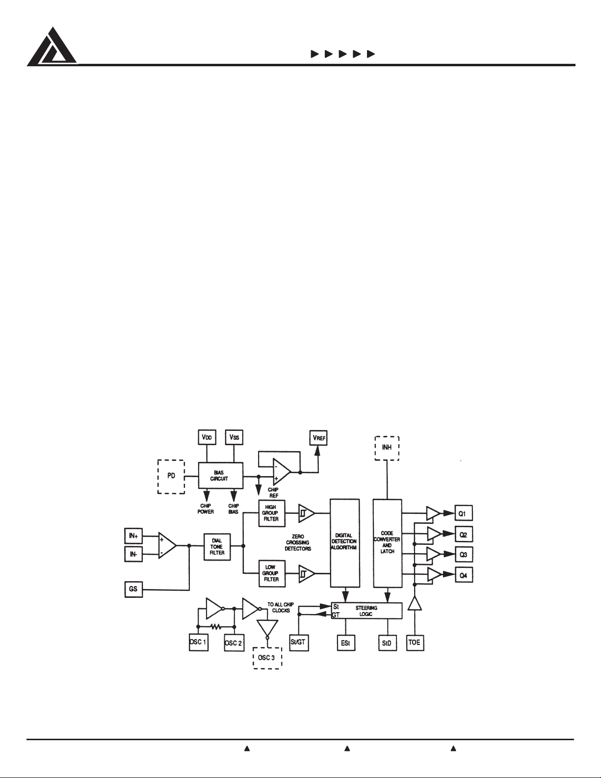
The CAMD CM88L70/70C provides full DTMF receiver capability by integrating both the bandsplit filter and digital decoder
functions into a single 18-pin DIP, SOIC, or 20-pin PLCC, TSSOP, or QSOP package. The CM88L70/70C is manufactured using
state-of-the-art CMOS process technology for low power consumption (35mW, max.) and precise data handling. The filter
section uses a switched capacitor technique for both high and low group filters and dial tone rejection. The CM88L70/70C
decoder uses digital counting techniques for the detection and decoding of all 16 DTMF tone pairs into a 4-bit code. This
DTMF receiver minimizes external component count by providing an on-chip differential input amplifier, clock generator, and
a latched three-state interface bus. The on-chip clock generator requires only a low cost TV crystal or ceramic resonator as
an external component.
Applications
PCMCIA
Portable TAD
Mobile radio
Remote control
Remote data entry
Call limiting
Telephone answering systems
Paging systems
Block Diagram
© 2000 California Micro Devices Corp. All rights reserved.
6/16/2000
215 Topaz Street, Milpitas, California 95035 Tel: (408) 263-3214 Fax: (408) 263-7846 www.calmicro.com
C0451098
1
CALIFORNIA MICRO DEVICES
CM88L70/70C
Absolute Maximum Ratings: (Note 1)
This device contains input protection against
damage due to high static voltages or
electric fields; however, precautions should
be taken to avoid application of voltages
higher than the maximum rating.
Note:
1. Exceeding these ratings may cause
permanent damage, functional
operation under these conditions is not
VSS)
retemaraPlobmySeulaV
-
V(egatloVylppuSrewoP
DD
niPynanoegatloVV
niPynanotnerruCI
erutarepmeTegarotST
V
DD
t
t
S
V
SS
SGNITARMUMIXAMETULOSBA
xaMV0.6
VotV3.0-
V3.0+
DD
xaMAm01
C°051+otC°56-
implied.
DC Characteristics: All voltages referenced to VSS, VDD = 3.0V + 20% / -10%, TA = -40°C to +85°C unless otherwise noted.
SCITSIRETCARAHCCD
retemaraPlobmySniMpyTxaMstinUsnoitidnoCtseT
egatloVylppuSgnitarepOV
tnerruCylppuSgnitarepOI
tnerruCylppuSybdnatSI
DD
DD
SDD
7.20.36.3V V
0.30.5Am
0.501
µA
V=DP
DD
egatloVtupnIleveLwoLVLI0.1V VDDV0.3=
egatloVtupnIleveLhgiHV
tnerruCegakaeLtupnII
EOTnotnerruC)ecruoS(pUlluPI
DPtnerruC)knis(nwodlluPI
HNItnerruC)knis(nwodlluPI
)-NI,+NI(,ecnadepmItupnIR
egatloVdlohserhTgnireetSV
egatloVtuptuOleveLwoLV
egatloVtuptuOleveLhgiHV
tnerruC)ecruoS(hgiHtuptuOI
egatloVtuptuO
ecnatsiseRtuptuOR
V
FER
HIL/LI
V
HI
os
DP
HNI
NI
tsT
LO
HO
HO
FER
RO
0.2VV
21-0.2-
1.0
0.154
0.154
µA
µA
µA
µA
VNIV=
SS
V0.3=
DD
Vro
DD
V0=EOT
V0.3=DP
V0.3=NHI
01MΩ zHK1@
5.1V
1.04.0V ILOAm0.1=
4.26.2VI
0.1AmV
TUO
004= µA
HO
V@V5.2=
DD
5.1V daoLoN
01
ΩΚ
)11etoN(
V7.2=
Operating Characteristics: All voltages referenced to VSS, VDD = 3.0V + 20% / -10%, TA = -40°C to +85°C unless otherwise noted.
Gain Setting Amplifier
SCITSIRETCARAHCGNITAREPO
retemaraPlobmySniMpyTxaMstinUsnoitidnoCtseT
tnerruCegakaeLtupnII
ecnatsiseRtupnIR
egatloVtesffOtupnIV
noitcejeRylppuSrewoPRRSP0506Bd)21etoN(zHK1
noitcejeRedoMnommoCRRMC0406BdV<V0.3-
niaGegatloVpooLnepOCDA
gniwSegatloVtuptuOV
)SG(daoLeviticapaCelbareloTCL001Fp
)SG(daoLevitsiseRelbareloTR
©2000 California Micro Devices Corp. All rights reserved.
2
215 Topaz Street, Milpitas, California 95035 Tel: (408) 263-3214 Fax: (408) 263-7846 www.calmicro.com
NI
NI
SO
LOV
2356Bd
htdiwdnaBniaGytinUpooLnepOcf3.00.1zHM
O
L
)daoLoN(egnaRedoMnommoCmcV0.55.1V
001AnV
SS
01MΩ
5152Vm
2.2V
P-P
RL≥ K001 Ω Vot
KΩ
P-P
V<
V<
NI
DD
V0.3<
NI
SS
daoLoN
8/16/2000
CALIFORNIA MICRO DEVICES
CM88L70/70C
AC Characteristics: All voltages referenced to V
using test circuit (Fig. 1) unless otherwise noted.
retemaraPlobmySniMpyTxaMstinUsetoN
sleveLlangiStupnIdilaV
)langisetisopmocfoenothcae(
tpeccAtsiwTevitisoP 6Bd
tpeccAtsiwTevitageN 6Bd
timiLtpeccAnoitaiveD.qerF zH2±%5.1.moN01,8,5,3,2
timiLtcejeRnoitaiveD.qerF%5.3±.moN5,3,2
ecnareloTenoTdrihT 61-Bd41,31,9,8,5,4,3,2
ecnareloTesioN21-Bd9,8,6,5,4,3,2
ecnareloTenoTlaiD 22+Bd9,8,7,5,4,3,2
emiTnoitceteDtneserPenoTt
emiTnoitceteDtnesbAenoTt
tpeccAnoitaruDenoTniMt
tcejeRnoitaruDenoTxaMt
tpeccAesuaPtigidretnI.niMt
tcejeResuaPtigidretnI.xaMt
)QottS(yaleDnoitagaporPt
)DtSottS(yaleDnoitagaporPt
)DtSotQ(pUteSataDtuptuOt
elbanEt
)QotEOT(yaleDnoitagaporP
elbasiDt
ycneuqerFkcolC/latsyrCf
)2CSO(tuptuOkcolCeviticapaC
daoL
PD
AD
CER
CER
DI
OD
QP
SPtD
SQtD
ETP
DTP
KLC
C
OL
, VDD=3.0V + 20% / -10%, TA=-40°C to +85°C, f
SS
SCITSIRETCARAHCCA
63-4.6-mBd
3.21073Vm
58 41Sm
5.03 5.8Sm
04Sm
02Sm
04Sm
02
31
8
4.3
002Sn
005Sn
9575.35975.31385.3zHM
03Fp
µS
µS
µS
µS
=3.579545 MHz
CLK
SMR
R
C
8,5,4,3,2,1
otrefeR
margaiDgnimiT
)elbatsujdAresU(
eranwohssemiT
htiwdeniatbo
)1.giFnitiucric
V=EOT
DD
K01= Ω
L
L
Fp05=
Notes:
1. dBm = decibels above or below a reference power
of 1 mW into a 600 ohm load.
2. Digit sequence consists of all 16 DTMF tones.
3. Tone duration = 40mS. Tone pause = 40 mS.
4. Nominal DTMF frequencies are used.
5. Both tones in the composite signal have
an equal amplitude.
6. Bandwidth limited (0 to 3 KHz) Gaussian Noise.
7. The precise dial tone frequencies are
(350 Hz and 440 Hz) ±2%.
8. For an error rate of better than 1 in 10,000
© 2000 California Micro Devices Corp. All rights reserved.
6/16/2000
215 Topaz Street, Milpitas, California 95035 Tel: (408) 263-3214 Fax: (408) 263-7846 www.calmicro.com
9. Referenced to lowest level frequency component
in DTMF signal.
10. Minimum signal acceptance level is measured with
specified maximum frequency deviation.
11. Input pins defined as IN+, IN-, and TOE.
12. External voltage source used to bias V
13. This parameter also applies to a third tone injected onto
.
REF
the power supply.
14. Referenced to Figure 1. Input DTMF tone level
at -28 dBm.
3
 Loading...