

Page 1
1
This document is subject to change without notice.
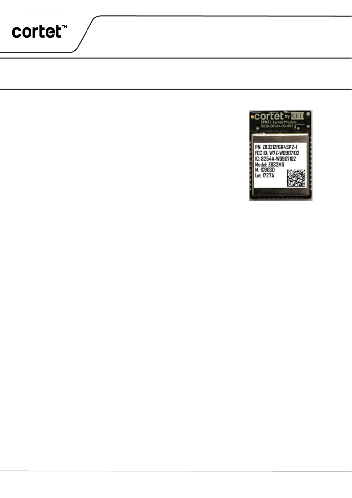
Zigbee®/Thread®/Bluetooth® Smart Mini Module
C
Module
PRELIMINARY DATASHEET
Embedded Multi-Protocol IOT Module
ZB3212F6R4SP2-1, ZB3212F6R4SP2-1
DESCRIPTION
The ZB3212F6R4SP2 ZigBee, Thread, Bluetooth Smart Mini Modules
feature the Silicon Labs EFR32MG12 single chip tra nsc eiver. These
devices are footprint-com patible with CEL’s existing line of ZigBee-,
Thread-, and Bluetooth-based modules, allowing f or fast and simple
performance upgrades via drop-in compatible hardware.
The ZB3212F6R4SP2 Mini Modules are fully certified standalone
solutions for designers looking to take advantage of the robustness of
the Silicon Labs Em berZNet PRO™ stack whil e having the f lexibility
to in terface to Blueto oth Smart-enabled devices previously deployed
in the field. These modules eliminate design risk and significantly
reduce time-to-market for a m ultitude of IoT applications.
These EFR32-based devices are compatible with Silicon Labs’
Simplicity Studio development environment which includes an eclipsebased IDE, documentation, debug, energy management tools, and
flashing tools. Simplicity Studio supports a multitude of sample
applications for m any common uses of the ERF32 , accelerating the
development proof-of-concept designs and demos.
KEY FEATURES
Multi-Protocol Support in a Single Device:
•
ZigBee 3.0, Thread, Bluetooth Smart 5.0
Enhanced Memory
•
1MB Flash
256kB SRAM
Up to 24 Analog/Digital GPIOs, including SPI,
•
USART, I2C, 12b ADC, iDAC, Comparators and
Timers
Radiated Output power up to 20dBm
•
Two Antenna Configurations
•
o
o
Mini Footprint: 0.940” x 0.655” (23.9 x 16.6mm)
•
Footprint-compatible with CEL's Bluetooth, ZigBee,
•
and Thread Module Family, Allowing for Fast and
Simple Performance Upgrades
ZB3212F6R4SP2-1 Variant FCC, IC, Certified* for
•
Usage Throughout North America and Canada
* Official FCC & IC certifications are in process and
Integrated PCB Trace Antenna
External Antenna Connections via 50Ω RF
Castellation Port for development
pending final approval by the respective
governmental bodies.
APPLICATIONS
•
•
•
•
•
•
•
•
Silicon Labs Mighty Gecko-Based
Connected Home & Appliances
Building Control & Automation
Lighting
Security
Wireless Sensor Networks
Wireless Audio & Video
Remote Health and Wellness Monitoring
General IoT Wireless Networking
Document No: 0020-00-07-00-000 (Issue A)
Date Published: September 11, 2017
Page 2

2
PRELIMINARY DATASHEET
TABLE OF CONTENTS
ZB3212F6R4SP2
DESCRIPTION ...................................................................................................................................... 1
KEY FEATURES ..................................................................................................................................... 1
TABLE OF CONTENTS ........................................................................................................................... 2
BLOCK DIAGRAM................................................................................................................................. 3
ORDERING INFORMATION ................................................................................................................... 3
ANTENNA ............................................................................................................................................ 4
RECOMMENDED OPERATING CONDITIONS .......................................................................................... 4
DC CHARACTERISTICS .......................................................................................................................... 5
RF CHARACTERISTICS ........................................................................................................................... 5
I/O PIN ASSIGNMENTS ........................................................................................................................ 6
CEL MINI MODULE COMPATIBILITY...................................................................................................... 7
MODULE DIMENSIONS ........................................................................................................................ 7
MODULE LAND FOOTPRINT ................................................................................................................. 8
PROCESSING ....................................................................................................................................... 9
AGENCY CERTIFICATIONS ...................................................................................................................11
SHIPMENT, HANDLING AND STORAGE ................................................................................................12
QUALITY ............................................................................................................................................12
REVISION HISTORY .............................................................................................................................13
DISCLAIMER .......................................................................................................................................13
This document is subject to change without notice.
Document No: 0020-00-07-00-000 (Issue A)
Page 3
3
PRELIMINARY DATASHEET
Order Number
Description
Min/Multiple
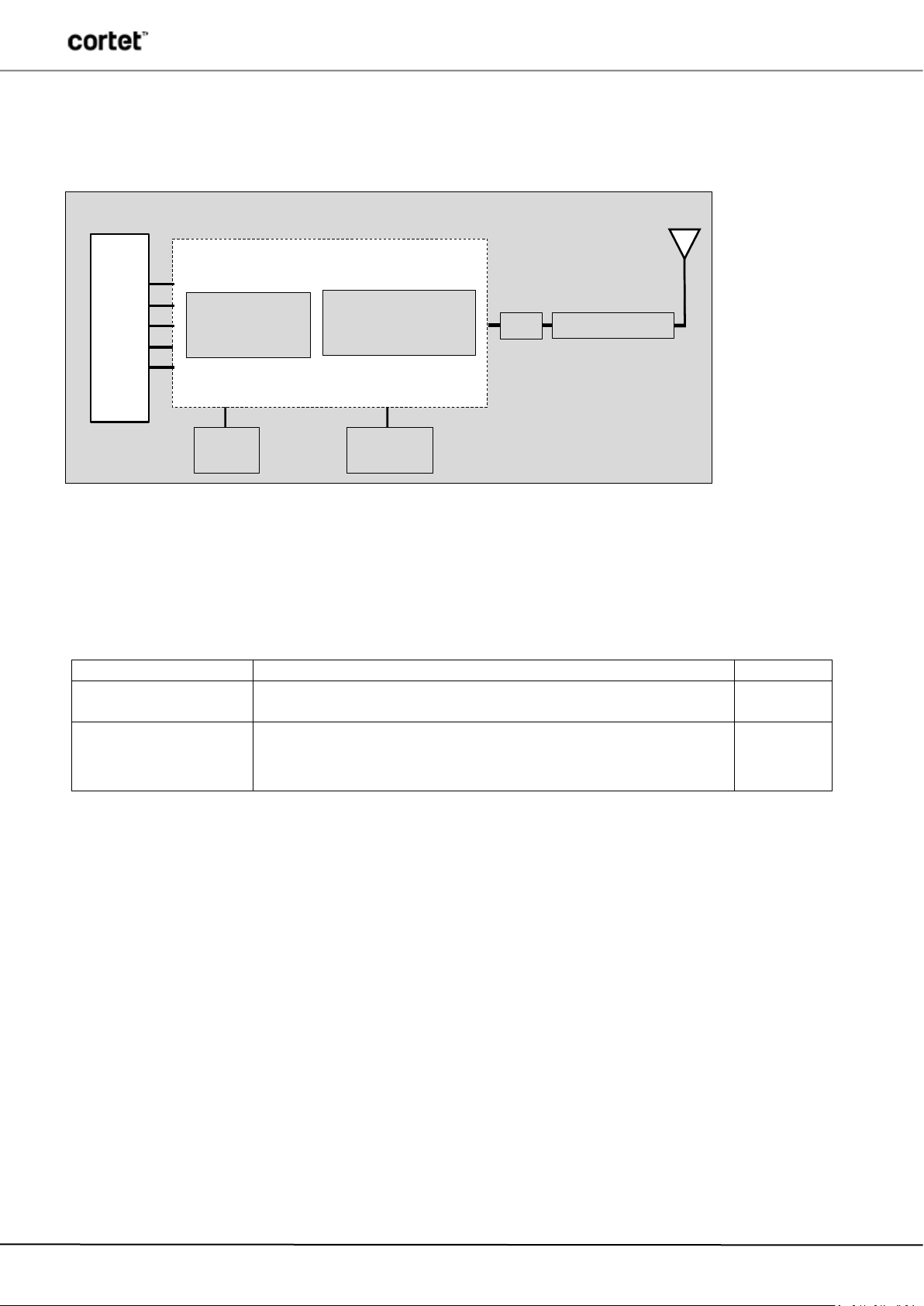
single chip transceiver + MCU (1MB flash, 256kB RAM), Trace Antenna
Zigbee/Thread/BT Smart Module, EFR32MG12P433F1024GM48-C0
PLACING ON THE MARKET.
EFR32MG12P432F1024GM48
Radio Transceiver
ARM Cortex M4
LPF
Antenna Match
32 KHz
Crystal
38.4 MHz
Crystal
Cortet Module
Edge
Castellation
2405 – 2480
MHz
VCC
GND
SPI
I2C
TIMER
USART
ADC
GPIO
DEBUG
BLOCK DIAGRAM
ZB3212F6R4SP2
ORDERING INFORMATION
ZB3212F6R4SP2-1-R
ZB3212F6R4SP2-1C-R
Zigbee/Thread/BT Smart Module, EFR32MG12P433F1024GM48-C0
single chip transceiver + MCU (1MB flash, 256kB RAM), Castellation Pin
for External Antenna.
NOT FCC OR IC CERTIFIED. END USER MUST CERTIFY BEFORE
600
600
This document is subject to change without notice.
Document No: 0020-00-07-00-000 (Issue A)
Page 4
4
PRELIMINARY DATASHEET
ZB3212F6R4SP2
Power Supply Voltage
0
3.8
V
VDD+2
Voltage on any non-5V Tolerant IO Line
-0.3
VDD+0.3
V
RF Input Power
-
10
dBm
Storage Temperature
-50
150
°C
Reflow Soldering Temperature
-
260
°C
2480
ANTENNA
The Cortet Mini Modules include an integrated Printed Circuit Board (PCB) trace antenna certified for FCC & IC requirements.
An optional configuration which uses a castellation pin on the module allows the user to connect to an external ante nna however
this implementation would require certification by the end user and may not use the CEL FCC ID number on the label. The PCB
antenna employs a topology that is compact and highly efficient. To maximize range, an adequate ground plane must be
provided on the host PCB. Correctly positioned, the ground plane on the host PCB will contribute significantly to the antenna
performance.
For optimum antenna performance, the Cortet Mini Module should be mounted with the PCB trace antenna overhanging the
edge of the host board and ideally in the upper left corner of the host board so that free space is left of the module as opposed to
additional pcb and components. To further improve performance, a ground plane may be placed on the host board under the
module, up to the antenna but not extending under the antenna (a minimum of 1.5" x 1.5" is recommended). The installation of
an uninterrupted ground plane on a layer directly beneath the module will also allow traces to be routed under the layer. Refer to
the application note
Mini Modules Hardware Design Guidelines
for more details. CEL can assist with your PCB layout.
The following are some design guidelines to help ensure optimal ant e nna performance:
The antenna portion of the Mini Module should hang over the host board so that there is not any additional
•
PCB under the antenna.
Never place the antenna close to metallic objects
•
In the final assembly, ensure that wiring and other components are not placed near the antenna
•
Do not place the antenna in a metallic or metalized plastic enclosure
•
Keep plastic enclosures a minimum of 1cm away from the antenna in any direction
•
Under Industry Canada regulations, this radio transmitter may only operate using an antenna of a type and maximum (or lesser)
gain approved for the transmitter by Industry Canada. To reduce potential radio interference to other users, the antenna type and
its gain should be so chosen that the equivalent isotropically radiated power (e.i.r.p.) is not more than that necessary for
successful communication.
Conformément à la réglementation d'Industrie Canada, le présent émetteur radio peut fonctionner avec une antenne d'un type et
d'un gain maximal (ou inférieur) approuvé pour l'émetteur par Industrie Canada. Dans le but de réduire les risques de brouillage
radioélectrique à l'intention des autres utilisateurs, il faut choisir le type d'antenne et son gain de sorte que la puissance isotrope
rayonnée équivalente (p.i.r.e.) ne dépasse pas l'intensité nécessaire à l'établissement d'une communication satisfaisante.
ABSOLUTE MAXIMUM RATINGS
Description Min Max Unit
Min of
Voltage on any 5V Tolerant IO Line -0.3
5.25 and
RECOMMENDED OPERATING CONDITIO NS
Symbol Parameter Min Typ Max Unit
Power Supply Voltage
Frequency 2405
Ambient Temperature Range -40
2.4 3.3 3.8 V
85 °C
V
MHz
This document is subject to change without notice.
Document No: 0020-00-07-00-000 (Issue A)
Page 5

5
PRELIMINARY DATASHEET
Item
Condition
Min
Nom
Max
Unit
120
A/MHz
Item
Condition
Nom
Unit
Item
Condition
Nom
Unit
DC CHARACTERISTICS
(@ 3.3VDC and 25°C unless otherwise specified)
ZB3212F6R4SP2
Tx Mode: 2.4 GHz 19.5 dBm1 Continuously Modulated Carrier
Tx Mode: 2.4 GHz 10 dBm1 Continuously Modulated Carrier
Tx Mode: 2.4 GHz 0 dBm1 Continuously Modulated Carrier
Rx mode
Sleep Modes
1. Power referenced at the IC output.
802.15.4
Bluetooth Smart
EM1 all peripherals disabled
EM2 deep sleep mode
EM3 stop mode
EM4 Hibernate mode
55
18
12
12
65
2.8
2.7
0.62
RF CHARACTERISTICS
TRANSMITTER
Maximum Radiated TX Power 3.8 V supply 20 dBm
Minimum TX Power Power Setting -20 or less -25 dBm
Frequency Range
The RF performance reported above assumes a default supply voltage of 3.3V unless otherwise noted.
2400 - 2483.5 MHz
RECEIVER
mA
mA
mA
mA
mA
µ
µA
µA
µA
1% PER 802.15.4 250kbps -101 dBm
1 % PER Sensitivity 2Mbps 2GFSK signal -89.2 dBm
0.1 % BER Sensitivity 250kbps 2GFSK signal -99.1 dBm
Frequency Range
This document is subject to change without notice.
Document No: 0020-00-07-00-000 (Issue A)
2400 - 2483.5 MHz
Page 6

6
PRELIMINARY DATASHEET
I/O PIN ASSIGNMENTS
3
PA0
5
PA1
6
PA2
7
PA3
8
PA5/US0_SCLK/CTS
9
PB11/US0_CS/RTS
11
PB13/Wake/US1_RX/I2C0_SDA
15
PC7/US1_CS
16
PC8
17
PC9
19
PC11/I2C0_SDA/US0_TX
20
PF4/I2C0_SCL/US0_RX
22
PF2/JTDO/SWO
23
PF3/JTDI
25
PF5
28
PD13/APCY/APDX
Could be A/D or GPIO
30
PD15/APCY/APDX
Could be A/D or GPIO
Refer to the STM32 datasheet for pin functionality details.
ZB3212F6R4SP2
Module Pin
Number
1, 2, 12, 31,
33
4 Reset
10 PB12/US1_TX
13 VCC Input power to the module.
14 PC6/I2C0_SCL/US1_CLK
18 PC10/
Pin Name Notes
GND
21 PF0/JTCK/SWCLK
24 PF1/JTMS/SWDIO
26 PF6/APBY/APAX Could be A/D or GPIO
27 PF7
29 PD14/APDY/APCX Could be A/D or GPIO
32 RF OUT Castellation Pin for External Antenna
This document is subject to change without notice.
Document No: 0020-00-07-00-000 (Issue A)
Page 7

7
PRELIMINARY DATASHEET
ZB3212F6R4SP2
Pin #
Function
ZICM35x
B1010
ZB3212F6R4SP2
4
Reset
RESET
N/C
RESET
7
Wake
PA7
WAKE
PA3
8, 9, 19, 20
Serial Controller 1
UART/SPI/I2C
Two wire UART/I2C
USART/I2C
10, 11, 14,
Serial Controller 2
SPI/I2C
I2C
SPI/I2C
16, 17, 21,
Debug &
Debug &
Debug &
Debug &
28, 30
ADC
PB7, PB5
AIO[1], AIO[2]
PD13, PD15
29
Timer
PB6
PIO[11]
PD14
CEL MINI MODULE COMPATIBILITY
The geometry of the land pattern and location of the RF castellations is identical to CEL’s ZICM35x family of ZigBee/Thread and
B1010 Bluetooth Smart Mini Modules. The digital and ana log mapp ing to dev elop a drop-in com pati ble so luti on is des crib ed
below:
15
22, 23, 24,
27
Programming
MODULE DIMENSIONS
Programming
Programming
Programming
This document is subject to change without notice.
Document No: 0020-00-07-00-000 (Issue A)
Page 8

8
PRELIMINARY DATASHEET
MODULE LAND FOOTPRINT
ZB3212F6R4SP2
This document is subject to change without notice.
Document No: 0020-00-07-00-000 (Issue A)
Page 9

9
PRELIMINARY DATASHEET
Parameter Values
Ramp Up Rate (from T
soakmax
to T
peak
)
3º/sec max
Minimum Soak Temperature
150ºC
Maximum Soak Temperature
200ºC
Soak Time
60-120 sec
T
Liquidus
217ºC
Time above T
Liquidus
60-150 sec
T
peak
250ºC
Time within 5º of T
peak
20-30 sec
Time from 25º to T
peak
8 min max
Ramp Down Rate
6ºC/sec max
PROCESSING
Recommended Reflow Profile
ZB3212F6R4SP2
Pb-Free Solder Paste
Use of “No Clean” soldering paste is strongly recommended, as it does not require cleaning after the soldering process.
Note:
The quality of solder joints on the castellations ("half vias") where they contact the host board should meet the
appropriate IPC Specifi cation. See the Caste llated Terminati ons Section in the l atest IPC-A-610 Accept ability of Electr onic
Assemblies document.
Cleaning
In general, cleaning the populated module is strongly discouraged. Residuals under the module cannot be easily removed with
any cleaning process.
• Cleaning with water can lead to capillary effects where water is absorbed into the gap between the host
board and the module. The combination of soldering flux residuals and encapsulated water could lead to short circuits
between neighboring pads. Water could also damage any stickers or labels.
• Cleaning with alcohol or a similar organic solvent will likely flood soldering flux residuals into the two
housings, which is not accessible for post-washing inspection. The solvent could also damage any stickers or labels.
• Ultrasonic cleaning could damage the module permanently.
The best approach is to consider using a “No Clean” solder paste and eliminate the pos t -so l dering clean ing ste p.
Optical Inspection
After soldering the module to the host board, consider optical inspection to check the following:
• Proper alignment and centering of the module over the pads
• Proper solder joints on all pads
• Excessive solder or contacts to neighboring pads or vias
Repeating Reflow Soldering
Only a single reflow soldering process is encouraged for host boards.
This document is subject to change without notice.
Document No: 0020-00-07-00-000 (Issue A)
Page 10

10
PRELIMINARY DATASHEET
ZB3212F6R4SP2
Wave Soldering
If a wave soldering pr ocess is r equired o n the host boards due to the pr esence of leaded co mponents, only a singl e wav e soldering
process is encouraged.
Hand Soldering
Hand soldering is possible. When using a soldering iron, follow IPC recommendations (reference document
IPC-7711
).
Rework
The Cortet module can be unsoldered from the host board. Use of a hot air rework tool should be programmable and the solder
joint and module should not exceed the maximum peak reflow temperature of 250ºC.
Caution
If temperature ramps exceed the reflow temperature profile, module and component damage may occur due to thermal shock.
Avoid overheating.
Warning
Never attempt a rework on t he module itself (i.e., replacing indiv idual compo nent s); suc h action s will ter minat e war ranty co verage.
Additional Grounding
Attempts to improve the module or the system grounding by soldering braids, wires or cables onto the module RF shield cover is
done at the customer's own risk. The ground pins at the module perimeter should be sufficient for optimum immunity to external
RF interference.
This document is subject to change without notice.
Document No: 0020-00-07-00-000 (Issue A)
Page 11

11
PRELIMINARY DATASHEET
ZB3212F6R4SP2
AGENCY CERTIFICATIONS
NOTE: Certifications are in process and pending final approval
FCC Compliance Statement Part 15.19, Section 7.15 of RSS-GEN
This device complies with Part 15 of the FCC Rules and with Industry Canada licence-exempt RSS Standards. Operation is
subject to the following two conditions:
1. This device may not cause harmful interference, and
2. This device must accept any interference received, including interference that may cause undesired operation.
Le présent appareil est conforme aux CNR d'Industrie Canada applicables aux appareils radio exempts de licence. L'exploitation
est autorisée aux deux conditions suivantes:
1. l'appareil ne doit pas produire de brouillage, et
2. l'utilisateur de l'appareil doit accepter tout brouillage radioélectrique subi, même si le brouillage est susceptible d'en
compromettre le fonctionneme nt.
Warning (Part 15.21)
Changes or modifications not expressly approved by CEL could void the user's authority to operate the equipment.
20cm Separation Dist ance
To comply with FCC/IC RF exposure limits for general population/uncontrolled exposure, the antenna(s) used for this transmitter
must be installed to provide a separation distance of at least 20cm from all persons and must not be operated in conjunction with
any other antenna or transmitter.
OEM Responsibility to the FCC and IC Rules and Regulations
The Cortet Mini Module has been certified per FCC Part 15 Rules and to Industry Canada license exempt RSS Standards for
integration into products without further testing or certification. To fulfill the FCC and IC certification requirements, the OEM of the
Cortet Module must ensure that the information provided on the Cortet label is placed on the outside of the final product. The
Cortet Mini Module is labeled with its own FCC ID number and IC ID number. If the FCC ID and the IC ID are not visible when
the module is installed inside another device, then the outside of the device into which the module is installed must also display a
label referring to the enclosed module. The exterior label can use wording such as the following
“Contains Transmitter Module FCC ID: W7Z-WB4343S”
“Contains Transmitter Module IC: 8254A-WB4343S"
The OEM of the Cortet Mini Module may only use the approved antennas (PCB Trace Antenna) that have been certified with this
module. The OEM of the Cortet Mini Module must test their final product configuration to comply with Unintentional Radiator
Limits before declaring FCC Compliance per Part 15 of the FCC Rules.
IC Certification — Industry Canada Statement
The term "IC" before the certification/registration number only signifies that the Industry Canada technical specifications were
met.
Certification IC — Déclaration d'Industrie Canada
Le terme "IC" devant le numéro de certificat i on/d' e nregi str e ment si gnif ie seul em ent que le s spéc ifi cati ons techni que s Industrie
Canada ont été respectées.
Section 14 of RSS-210
The installer of this radio equipment must ensure that the antenna is located or pointed such that it does not emit RF field in
excess of Health Canada limits for the general population. Consult Safety Code 6, obtainable from Health Canada's website:
http://www.hc-sc.gc.ca/ewh-semt/pubs/radiation/radio_guide-lignes_direct-eng.php
L'article 14 du CNR-210
Le programme d'installation de cet équipement radio doit s'assurer que l'antenne est située ou orientée de telle sorte qu'il ne
pas émettre de champ RF au-delà des limites de Santé Canada pour la population générale. Consulter le Code de sécurité 6,
disponible sur le site Web de Santé Canada: http://w w w . hc-sc.gc.ca/ewh-semt/pubs/radiation/radio_guide-lignes_direct-eng.php
This document is subject to change without notice.
Document No: 0020-00-07-00-000 (Issue A)
Page 12

12
PRELIMINARY DATASHEET
SHIPMENT, HANDLING AND STORAGE
Shipment
The Cortet modules are delivered in reels of 600 units. The reel diameter is 12.992 inches ( 330m m).
ZB3212F6R4SP2
Handling
The Cortet modules are designed and packaged to be processed in an automated assembly line.
Warning
The Cortet modules contain highly sensitive electronic circuitry. Handling without proper ESD protection may destroy or damage
the module permanently.
Warning
The Cortet modules are moisture-sensitive devices. Appropriate handling instructions and precautions are summarized in J-STD-
033. Read carefully to prevent permanent damage due to moisture intake.
Moisture Sensitivity Level (MSL)
MSL 3, per J-STD-033
Storage
Storage/shelf life in sealed bags is 12 months at <40°C and <90% relative humidity.
QUALITY
CEL modules offer the highest quality at competitive prices. Our modules are manufactured in compliance with the IPC-A-610
specification, Class II. Our modules go through JESD22 qualification processes which includes high temperature operating life
tests, mechanical shock, temperature cycling, humidity and reflow testing.
CEL builds the quality into our products, giving our customers confidence when integrating our products into their systems.
This document is subject to change without notice.
Document No: 0020-00-07-00-000 (Issue A)
Page 13

13
PRELIMINARY DATASHEET
REVISION HISTORY
Previous Versions
Changes to Current Version
Page(s)
(Issue A) September 2017
The information in this document is current as of the published date. The information is subject to change without notice. For act ual
ZB3212F6R4SP2
0020-00-07-00-000
Initial Preliminary Data Sheet N/A
DISCLAIMER
design-in, refer to the latest publications of CEL Data Sheets or Data Books, etc., for the most up-to-date specifications of CEL products.
Not all products and/or types are available in every country. Please check with a CEL sales representative for avail ability and addit ional
information.
No part of this document may be copied or reproduced in any form or by any means without the prior written consent of CEL.
CEL assumes no responsibility for any errors that may appear in this document.
CEL does not assume any liability for infringement of patents, copyrights or other intellectual property rights of third parties by or arising
from the use of CEL products listed in this document or any other liability arising from the use of such products. No license, express,
implied or otherwise, is granted under any patents, copyrights or other intellectual property rights of CEL or others.
Descriptions of circuits, software and other related inf ormation in this document are provided for i llustrative purposes in semiconductor
product operation and application examples. The incorporat ion of these circuits, soft ware and information in t he design of a customer’s
equipment shall be done under the full responsibility of the customer. CEL assumes no responsibility for any losses incurred by customers
or third parties arising from the use of these circuits, software and information.
FOR MORE INFORMATION
For more information about CEL Cortet products and solutions, visit our website at cortet.cel.com.
TECHNICAL ASSISTANCE
For Technical Assistance, visit cortet.cel.com/tech-support.
This document is subject to change without notice.
Document No: 0020-00-07-00-000 (Issue A)
 Loading...