california eastern laboratories MC-7831, MC-7832, MC-7833 Service Manual

NEC's 870 MHz GaAs CATV
PUSH-PULL AMPLIFIER
MC-7831
MC-7832
MC-7833
FEATURES
• GaAs ACTIVE DEVICES
• LOW DISTORTION
• HIGH LINEAR GAIN:
MC-7831 - GL = 18 dB MIN at f = 870 MHz
MC-7832 - GL = 22 dB MIN at f = 870 MHz
MC-7833 - GL = 25 dB MIN at f = 870 MHz
• LOW RETURN LOSS
• LOW GAIN CHANGE OVER TEMPERATURE
• SPECIFIED FOR 79, 110, and 132 CHANNELS
PERFORMANCE
• HIGH RELIABILITY AND RUGGEDNESS:
Withstands environmental extremes as well as Silicon
devices (Surge, ESD, Etc.)
DESCRIPTION
NEC's MC-7831, MC-7832, and MC-7833 are GaAs MultiChip Modules designed for use as input stages in CATV applications up to 870 MHz. The only difference between these
devices is gain, which is 18 dB, 22 dB, and 25 dB respectively. Because these units are GaAs devices they have low
distortion, low noise figure, and low return loss across the entire
frequency band.
Like the previous generation of products, these devices survive such hazards as surge and ESD as well as their silicon
competitors, but deliver superior performance with low DC
current required. All devices are assembled and tested using
fully automated equipment to maximize consistency in part to
part performance, and reliability is assured by NEC's stringent quality and process control procedures. These parts come
in industry compatible hybrid packages.
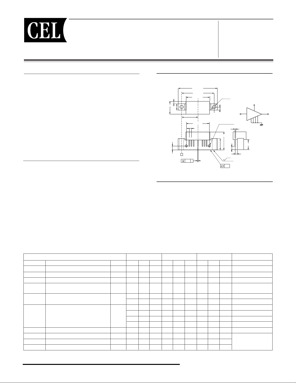
OUTLINE DIMENSIONS (Units in mm)
PACKAGE OUTLINE H02
45.08 MAX
14.85 MAX
3.2 MAX
8.1 MAX
4.19
38.1±0.25
27.5 MAX
19.05±0.38
25.4±0.25
2.54
±
0.25
12 3 5 789
±
0.13
A
0.38.. A
4.25
4.0±0.25
6-32 unc 2B
21.5 MAX
12.9 MAX
6.3
±
+ 0.25
- 0.35
2.62–0.35
2.5
0.05
In Out
0.51±0.050
2.54
APPLICATIONS
• CATV HEADEND SYSTEMS
• CATV OPTICAL NODES
• CATV DISTRIBUTION AMPS
2378
10.75±0.25
±
0.38
VDD
5
91
Gnd
ELECTRICAL CHARACTERISTICS (TA = 30±5 °C, VDD = 24 V, ZS = ZL = 75 Ω)
PART NUMBER MC-7831 MC-7832 MC-7833
SYMBOLS CHARACTERISTICS UNITS MIN TYP MAX MIN TYP MAX MIN TYP MAX TEST CONDITIONS
BW Frequency Range MHz 50 – 870 50 – 870 50 – 870
GL Linear Gain dB 18.0 – 19.0 22.0 – 23.0 25.0 – 26.0 f = 870 MHz
S Gain Slope dB 0.2 – 1.0 0.6 – 1.4 1.0 – 1.8 f = 40 to 870 MHz
Gf Gain Flatness dB – – 0.7 – – 0.7 – – 0.7 40 to 870 MHz;
Peak to Valley
NF Noise Figure 1 dB – – 6.5 – – 6.0 – – 5.5 f = 50 MHz
Noise Figure 2 – – 7.0 – – 6.5 – – 6.0 f = 870 MHz
RL Input/Output Return Loss dB 20.0 – – 20.0 – – 20.0 – – 40 to 160MHz
19.0 – – 19.0 – – 19.0 – – 160 to 320 MHz
17.5 – – 17.5 – – 17.5 – – 320 to 640 MHz
16.0 – – 16.0 – – 16.0 – – 640 to 870 MHz
IDD Operating Current mA 180 – 240 180 – 240 180 – 240 RF OFF
CTB Composite Triple Beat dBc – -59 -57 – -59 -57 – -59 -57 f = 40 to 870 MHz
XMod Cross Modulation1dBc dBc – -51 -50 – -53 -50 – -53 -50 110 Channels,
CSO Composite Second Order dBc – -63 -57 – -60 -57 – -61 -57 V
OUT = 44 dBmV, Flat
1. Measured per US standard methods and procedures (using selective level meter).
California Eastern Laboratories

MC-7831, 7832, 7833
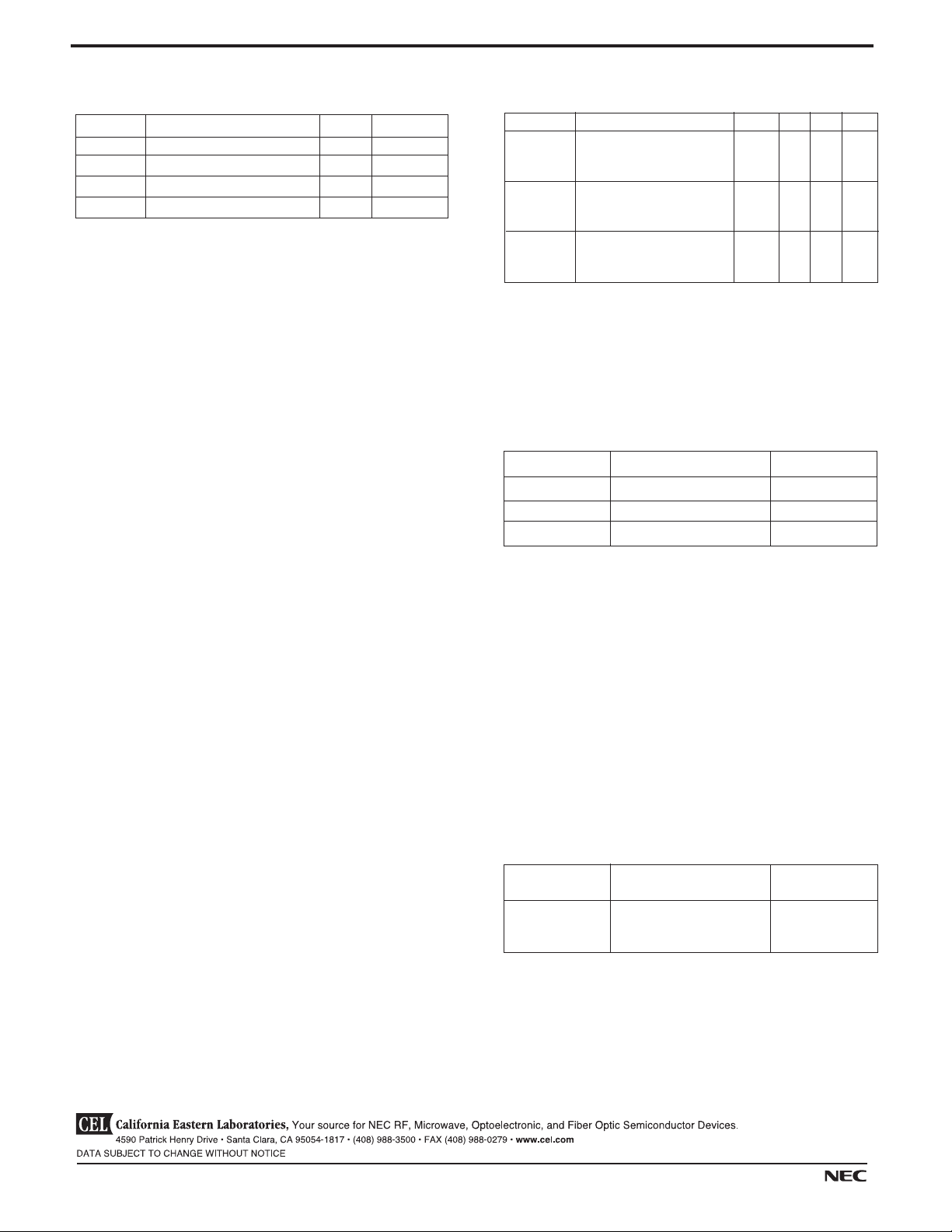
ABSOLUTE
MAXIMUM RATINGS1 (TCASE= 30 °C)
SYMBOLS PARAMETERS UNITS RATINGS
VDD Supply Voltage V 30
I Input Voltage
V
TC Operating Case Temperature °C -30 to +100
T
STG Storage Temperature °C -40 to +100
Note:
1. Operation in excess of any one of these parameters may result in
permanent damage.
2. Maximum single channel power applied to the input for 1 minute
with no measurable degradation in performance.
2
dBmV 65
RECOMMENDED
OPERATING CONDITIONS
SYMBOLS PARAMETERS UNITS MIN TYP MAX
DD Supply Voltage, MC-7831 V 23.5 24.0 24.5
V
V
i Input Voltage
TC Operating Case, MC-7831 °C -30 +25 +85
Note:
1. Test Conditions: 110 Channels, Flat
Temperature MC-7832 -30 +25 +85
MC-7832 23.5 24.0 24.5
MC-7833 23.5 24.0 24.5
1
, MC-7831 dBmV – 21.0 27.5
MC-7832 – 21.0 27.5
MC-7833 – 19.0 25.5
MC-7833 -30 +25 +85
(Zs = ZL = 75Ω)
ORDERING INFORMATION
PART NUMBER PACKAGE QUANTITY
MC-7831-AZ 7-pin special with heatsink 50pcs max/ Tray
MC-7832-AZ 7-pin special with heatsink 50pcs max/ Tray
MC-7833-AZ 7-pin special with heatsink 50pcs max/ Tray
NOTES ON CORRECT USE
1. The space between PC board and root of the lead should be
kept more than 1 mm to prevent undesired stress on the lead and
also should be kept less than 4 mm to prevent undesired parasitic
inductance.
Recommended space is 2.0 to 3.0 mm typical.
2. Recommended torque strength of the screw is 59 to 78 Ncm.
3. Form the ground pattern as wide as possible to minimize ground
impedance. (to prevent undesired oscillation)
All the ground pins must be connected together with wide ground
pattern to decrease impedance difference.
Life Support Applications
These NEC products are not intended for use in life support devices, appliances, or systems where the malfunction of these products can reasonably
be expected to result in personal injury. The customers of CEL using or selling these products for use in such applications do so at their own risk and
agree to fully indemnify CEL for all damages resulting from such improper use or sale.
RECOMMENDED SOLDERING CONDITIONS
This product should be soldered in the following recommended
conditions. Other soldering methods and conditions than the
recommended conditions are to be consulted with our sales
representatives.
Soldering Soldering Condition
Method Conditions Symbol
Pin Part Heating Pin area temperature: less –
than 260°C
Hour: Within 2 sec./pin
Note.
1. The point of pin part heating must be kept at a distance of more
than 1.2 mm from the root of lead.
1
A Business Partner of NEC Compound Semiconductor Devices, Ltd.
07/08/2003
 Loading...