

Page 1

Technical
Information
Manual
MOD. V1729
22 June 2005
Revision n. 3
4 CHANNEL/12BIT
SAMPLING ADC
MANUAL REV.3
NPO:
00109/04:V1729.MUTx/03
Page 2

CAEN will repair or replace any product within the guarantee period if the Guarantor declares
that the product is defective due to workmanship or materials and has not been caused by
mishandling, negligence on behalf of the User, accident or any abnormal conditions or
operations.
CAEN declines all responsibility for damages or
injuries caused by an improper use of the Modules due
to negligence on behalf of the User. It is strongly
recommended to read thoroughly the CAEN User's
Manual before any kind of operation.
CAEN reserves the right to change partially or entirely the contents of this Manual at any time
and without giving any notice.
Page 3

PRELIMINARY
Document type: Title: Revision date: Revision:
User's Manual (MUT) Mod. V1729 4 Channel 12 Bit Sampling ADC 22/06/2005 3
NPO: Filename: Number of pages: Page:
00109/04:V1729.MUTx/03 V1729_REV3.DOC 38 3
TABLE OF CONTENTS
1. GENERAL DESCRIPTION.......................................................................................................................5
1.1 OVERVIEW .............................................................................................................................................5
1.2 SAMPLING FREQUENCY ..........................................................................................................................6
1.3 INPUT SIGNALS, DYNAMIC RANGE..........................................................................................................6
2. OPERATING MODES...............................................................................................................................7
2.1 DEFINITION OF THE ACQUISITION WINDOW. TRIGGER MODES.................................................................7
2.1.1 Principle, PRETRIG, POSTTRIG..................................................................................................7
2.1.2 Trigger sources..............................................................................................................................8
2.1.3 Trigger edge ..................................................................................................................................8
2.1.4 TRIGOUT signal ...........................................................................................................................8
2.2 VALIDATION OF THE TRIGGER BY A SECOND SUBSEQUENT SIGNAL.........................................................9
2.3 DEAD TIME AT RESTARTING OF THE ACQUISITION; PRETRIG.................................................................10
2.4 STANDARD ACQUISITION SEQUENCE.....................................................................................................10
2.5 CORRECTION OF DATA..........................................................................................................................11
2.5.1 Correction of the pedestals..........................................................................................................12
2.5.2 Temporal corrections ..................................................................................................................13
3. SYNCHRONIZATIONS AND CALIBRATIONS.................................................................................16
3.1 SYNCHRONIZATION BETWEEN THE CHANNELS......................................................................................16
3.1.1 Channels from the same board....................................................................................................16
3.1.2 Channels situated on different boards........................................................................................16
3.2 SYNC_OUT AND BUSY SIGNALS ......................................................................................................16
3.3 CALIBRATIONS .....................................................................................................................................17
3.3.1 Calibration of the interpolator....................................................................................................17
3.3.2 Calibration of the pedestals.........................................................................................................20
3.3.3 Temporal calibration between different channels.......................................................................20
4. TECHNICAL SPECIFICATIONS..........................................................................................................21
4.1 PACKAGING..........................................................................................................................................21
4.2 SAMPLING FREQUENCY ........................................................................................................................21
4.3 INPUT SIGNALS, DYNAMIC RANGE........................................................................................................21
4.4 FRONT PANEL.......................................................................................................................................22
4.5 MECHANICAL AND ELECTRICAL STANDARDS........................................................................................23
4.5.1 Mechanical standard...................................................................................................................23
4.5.2 Electrical interfaces.....................................................................................................................23
4.5.3 Summary of front panel signals...................................................................................................24
4.5.4 Supplies .......................................................................................................................................25
4.5.5 Pinout of the non-standard connectors .......................................................................................25
4.5.6 Straps and resistor network sockets ............................................................................................26
4.5.7 Implementation of differential inputs ..........................................................................................26
4.5.8 Using a shifted input range .........................................................................................................27
4.6 INTERFACES .........................................................................................................................................28
4.6.1 VME interface..............................................................................................................................28
4.6.2 GPIB Interface.............................................................................................................................28
4.7 READING OF THE DATA IN THE RAM, MAPPING....................................................................................29
4.8 LIST OF THE SUB-ADDRESSES................................................................................................................31
4.9 SYNOPSIS OF THE BOARD......................................................................................................................35
5. SPECIFICATIONS AND PERFORMANCES....................................................................................... 37
6. BIBLIOGRAPHY .....................................................................................................................................38
Page 4

PRELIMINARY
Document type: Title: Revision date: Revision:
User's Manual (MUT) Mod. V1729 4 Channel 12 Bit Sampling ADC 22/06/2005 3
NPO: Filename: Number of pages: Page:
00109/04:V1729.MUTx/03 V1729_REV3.DOC 38 4
LIST OF FIGURES
FIG. 1.1: DATA FLOW IN THE BOARD...................................................................................................................5
FIG. 2.1: CHRONOGRAM OF THE STOPPING OF THE ACQUISITION.........................................................................7
FIG. 2.2: CENTERING OF THE TRIGGER IN THE ACQUISITION WINDOW FOR TWO POSTTRIG CASES...................7
FIG. 2.3: SIMPLIFIED DESCRIPTION OF THE TRIGGER SELECTION CHAIN ..............................................................9
FIG. 2.4: SIMPLIFIED DESCRIPTION OF THE TRIGGER VALIDATION SYSTEM........................................................10
FIG. 2.5: BLOCK DIAGRAM OF A STANDARD ACQUISITION ................................................................................12
FIG. 2.6: TWO POSSIBILITIES FOR DETECTION AND FOR TREATMENT OF THE REQUEST......................................13
FIG. 2.7: UNFOLDING OF THE CIRCULAR MEMORY ............................................................................................14
FIG. 3.1: DIAGRAM OF THE CALIBRATION OF THE VERNIERS.............................................................................18
FIG. 4.1: MOD. V1729 FRONT PANEL..............................................................................................................22
FIG. 4.2: IMPLEMENTATION OF THE CONNECTORS AND CONFIGURATION ELEMENTS ON THE V1729.................23
FIG. 4.3: SYNOPSIS OF THE V1729 BOARD........................................................................................................35
FIG. 4.4: SYNOPSIS OF AN ACQUISITION CHANNEL ON THE MATACQ BOARD .................................................36
Page 5
PRELIMINARY
Document type: Title: Revision date: Revision:
User's Manual (MUT) Mod. V1729 4 Channel 12 Bit Sampling ADC 22/06/2005 3
NPO: Filename: Number of pages: Page:
00109/04:V1729.MUTx/03 V1729_REV3.DOC 38 5
1. General description
1.1 Overview
The CAEN Mod. V1729 board is suited for acquisition of fast analog signals based on the
MATACQ (analog matrix) chip developed by collaboration of the CEA/DAPNIA and the
l’IN2P3/LAL [1].
The V1729 board, in the mechanical format VME double Europe, is compatible with
several standards of acquisition (VME A32/D32, A24/D16, and GPIB).
This board performs the coding of 4 analog channels of bandwidth up to 300MHz over 12
bits at a sampling frequency (Fe) reaching up to 2GHz and over a depth of 2520 usable
points.
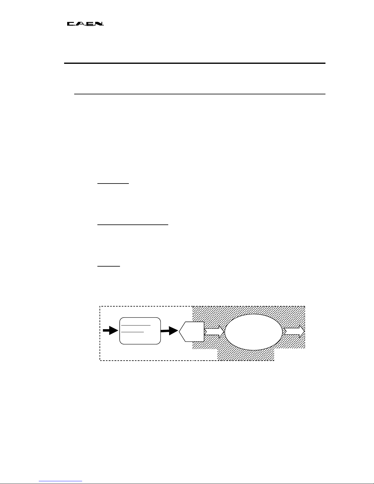
This operation is realized in three phases (see Fig 1.1):
Acquisition
:
the analog signal is continuously sampled at the frequency Fe in a circular analog
memory. The arrival of a trigger signal initiates the stopping phase of the sampling (2.1.1.
At the end of this phase, the state of the memory is set : it then contains the last 2560
points sampled (of which 2520 are valid).
Numerization and storage
:
after a stopping order of the acquisition, the samples stored under analog form in the
MATACQ chips are rapidly (650µs) re-read and coded into digital data over 12 bits, then
stored in a digital memory buffer. The acquisition is informed of the end of the coding
phase either by scrutation of an internal register, or by an interruption.
Reading
:
the memory buffer can then be re-read by the acquisition system. For an acquisition
system of VME A24-D16 standard, the latter operation lasts a few ms for the full readout
of a 4-channel board, which permits attaining an acquisition frequency of a few hundred
Hz for the acquisition of 2500 points per channel. With a high performance A32-D32
system, one should reach 1 kHz.
Fig. 1.1: data flow in the board
D
IGITAL ANALOG
SAMPLING
MATRIX
DIGITAL
MEMORY
BUFFER
ADC
Acquisition
Input
F
e = 1GS/s or 2GS/s
5 MHz
Up to 3MO/s in GPIB
and 20MO/s in VME
Page 6

PRELIMINARY
Document type: Title: Revision date: Revision:
User's Manual (MUT) Mod. V1729 4 Channel 12 Bit Sampling ADC 22/06/2005 3
NPO: Filename: Number of pages: Page:
00109/04:V1729.MUTx/03 V1729_REV3.DOC 38 6
1.2 Sampling frequency
The V1729 board is sequenced by an oscillator at a frequency of 100MHz. No greater
frequency signal exists on the board. This is what explains the low consumption of the
system. The sampling at a very high frequency (Fe) in the MATACQ chip is in fact
realized by virtual multiplication of frequency inside the chip by a factor up to 20.
The MATACQ chip functions with a pilot frequency of 50MHz or 100MHz programmable
on the board by software, which corresponds to a sampling frequency Fe (= 20*Fp) of 1
or 2 GHz.
The EXT_CLK input may possibly be used to inject a very clean external pilot clock
comprised between 50MHz and 100MHz.
Caution : the MATACQ chip cannot work properly with a pilot frequency Fp lower than
50MHz.
1.3 Input signals, Dynamic range
The V1729 board integrates 4 analog channels. The inputs of these channels are
connected through double LEMO plugs (IN0+/- to IN3+/-).
The inputs are by default unipolar and terminated on 50 Ohms. However, the input levels
of the board can be very easily modified (through displacing a few resistors and mounting
new ones) in such a way as to permit the input in differential mode (from which the
double LEMO plugs). For this purpose, free CMS-805 resistor footprints are indeed
implemented on the V1729 board.
The analog to digital conversion is made on 12 bits with a maximum dynamic range of
1V, or an LSB of 250μV. This range is centered on 0V (+/- 0.5V). However, free CMS805 footprints are implemented on the V1729 board for shifting the dynamic range in the
interval +/- 0.5V in order to be able to optimize the system for unipolar signals.
The measured noise referred to input is less than 200 μV RMS (i-e below the lsb of the
ADC), and the non-linearity remains below 1 per 1000 over the whole dynamic range.
Page 7
PRELIMINARY
Document type: Title: Revision date: Revision:
User's Manual (MUT) Mod. V1729 4 Channel 12 Bit Sampling ADC 22/06/2005 3
2. Operating modes
2.1 Definition of the acquisition window. Trigger modes
2.1.1 Principle, PRETRIG, POSTTRIG
During the acquisition, the analog signal is continuously sampled in the analog memory
which is comparable to a circular buffer with a depth of 2560 points (time depth =
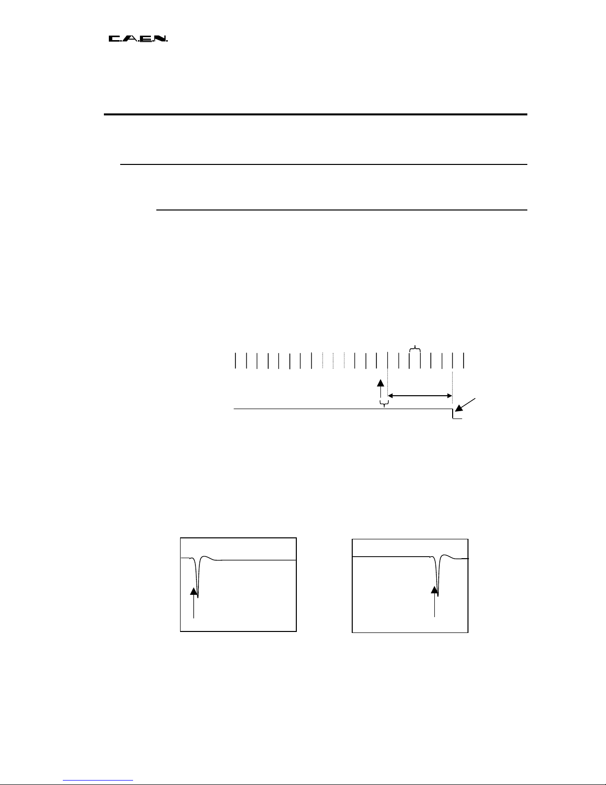
2560/Fe). The stopping of sampling is initiated by the arrival of a trigger signal Ta
(asynchronous trigger) which is common to all the channels of a board. This signal is
only authorized to be produced following a programmable time named PRETRIG after
the triggering of the acquisition sequence.
The effective stopping of the sampling will occur following a pre-defined number (named
POSTTRIG) of clock periods (50MHz or 100MHz) after the trigger (see Fig. 2.1).
Fig. 2.1: chronogram of the stopping of the acquisition
The POSTTRIG, programmable by the user, permits defining and displacing the position
of the trigger signal in the acquisition window. It is adjustable in the 1/Fp to 65535/Fp
range by steps of 1/Fp ( = 20ns or 10ns). This is illustrated in Fig 2.2.
In the example illustrated by Fig 2.2, the POSTTRIG is fixed at 6/Fp. The acquisition will
be stopped 6/Fp + ti after the arrival of the trigger signal (ti corresponds to the time
measured by the vernier between the Ta and the next rising edge of the clock). The
analog memory will then contain the 2560 last samples (of which only 2520 will be
exploited).
Fig. 2.2: centering of the Trigger in the acquisition window for two POSTTRIG cases
Thus, a POSTTRIG value close to 64 assures the centering of the trigger in the middle of
the acquisition window. For the values of POSTTRIG > 127, the trigger is no longer in the
acquisition window.
1/Fp
Rising Edge of Oscillator
Clock
Ta
ti
Acquisition
Stopping of
acquisition
POSTTRIG : here
= 6/Fp
Ta
Ta
High value of POSTTRIG
Low value of POSTTRIG
Asynchronous trigger
Page 8

PRELIMINARY
Document type: Title: Revision date: Revision:
User's Manual (MUT) Mod. V1729 4 Channel 12 Bit Sampling ADC 22/06/2005 3
NPO: Filename: Number of pages: Page:
00109/04:V1729.MUTx/03 V1729_REV3.DOC 38 8
2.1.2 Trigger sources
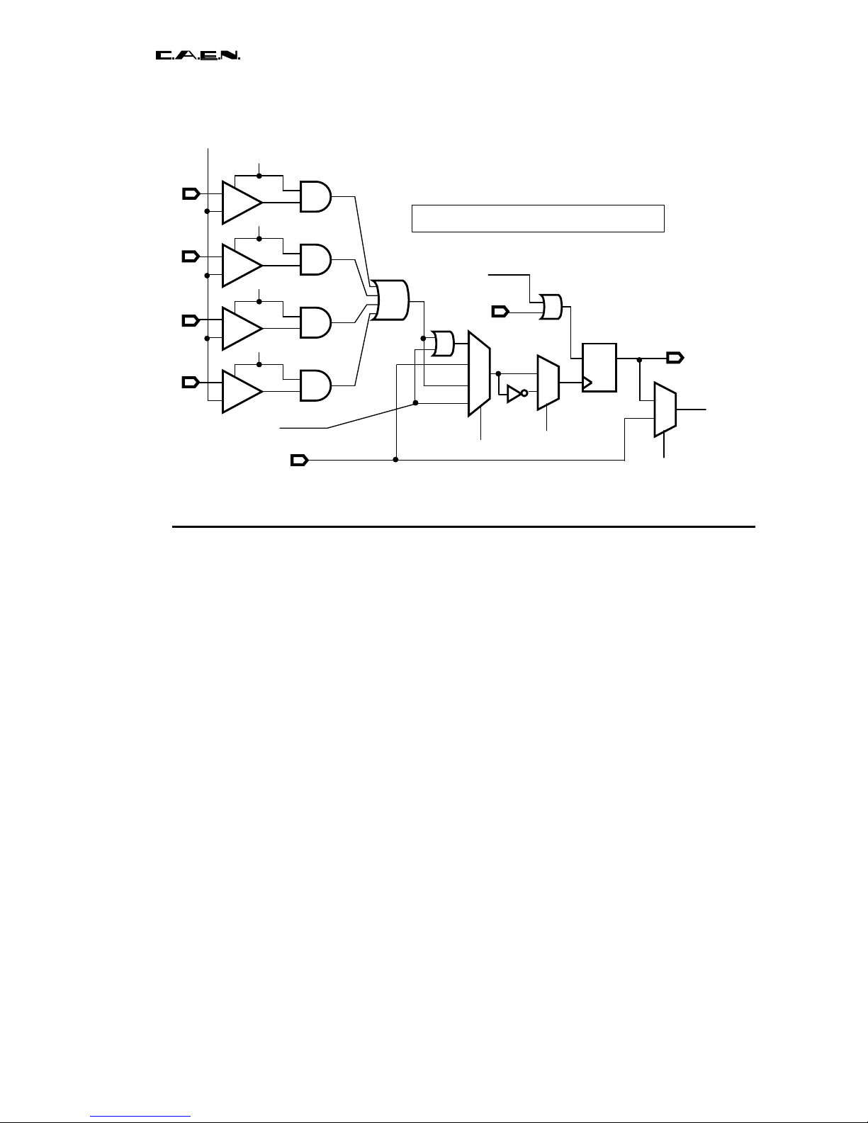
There are four possible sources for the trigger signal Ta. They are selectable by the user:
Trigger on signal
: this is the result of the logic « OR » of the discriminators on the
analog signals of one or several channels of the board by choice of the user. The
common threshold of the discriminators is programmable by steps of 0.25 mV over a
range of ± 0.5V (which corresponds to the integrality of the usable input range of the
board). The user can also define the type of discrimination (signal higher than or inferior
to the threshold) via the choice of the trigger edge.
External trigger
: external trigger signal entering on a LEMO plug (EXT_TRIG signal at
the NIM level). This signal can be either used as any other trigger source with choice of
its edge, or exploited directly as an asynchronous trigger (rising edge only) in cases
where one uses discriminators from several boards in order to produce at the exterior of
the boards (via their output TRIG_OUT) a trigger which will be sent back to them in a
synchronous way (see figure 2.2). This mode is selected by the bit 4 of the TRIG_TYPE
register.
Auto trigger
: triggered by a software command issued from the acquisition. It permits
the generation of a random trigger. This corresponds to the automatic trigger mode.
- « Auto + normal » trigger
: result of a logic « OR » between the trigger on signal and
the automatic trigger.
- Internal random trigger
: this internal periodic signal, asynchronous of the clock, can
be enabled or disabled. When it is enabled and the trigger mode selected is « auto », this
signal serves as a source for the automatic trigger. One uses it for the fast calibration of
the verniers of the MATACQ chips.
2.1.3 Trigger edge
The trigger edge (rising or falling) can be selected in all modes (except the direct external
trigger which uses only the rising edge).
2.1.4 TRIGOUT signal
A copy of the pre-trigger signal (positive pulse) generated by the V1729 board is
available at the output on a LEMO plug on the front panel (TRIG_OUT output on the NIM
level). It can in particular permit synchronization of trigger for several boards.
A simplified summary of the trigger modes of the board is presented in fig 2.3.
Page 9
PRELIMINARY
Document type: Title: Revision date: Revision:
User's Manual (MUT) Mod. V1729 4 Channel 12 Bit Sampling ADC 22/06/2005 3
NPO: Filename: Number of pages: Page:
00109/04:V1729.MUTx/03 V1729_REV3.DOC 38 9
Fig. 2.3: simplified description of the trigger selection chain
2.2 Validation of the trigger by a second subsequent signal.
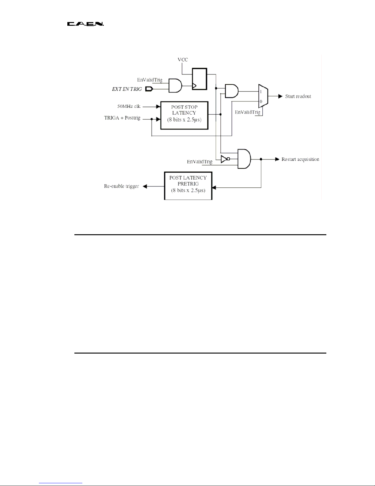
In the case where one would like to validate the data stored in the MATACQ chips before
their transfer towards the RAM, it is possible to make use of the EXT_EN_TRIG input to
introduce therethrough a validation signal (see figure 3c). This is particularly useful if the
system produces such a signal with a delay greater than the maximum sampling depth
(2560/Fp i-e 1.25μs at 2GS/s and 2.5μs at 1GS/s) and smaller than the transfer time
towards the RAM (650μs). This can thus permit a big decrease of the potential dead-time
linked to the readout. In this case, the usual use of the EXT_EN_TRIG signal (which
permits inhibiting the trigger as described on figure 3b) is inhibited.
In order to perform the validation, a programmable 8-bit latency counter ( called
POST_STOP_LATENCY) with steps of 2.5μs is started at the end of the POSTTRIG,
and if the external validation signal hasn’t arrived before the end of that delay, the
Matacq chips switch back into the analog input signal writing mode thus waiting for the
next trigger. If on the other hand the validation signal did arrive, the waiting data is
digitized then stored into the RAM. This mode is validated thanks to the bit 5 of the
TRIGGER_TYPE register (see IV.4). Moreover, a second 8-bit register ( called
POST_LATENCY_PRETRIG) with the same steps of 2.5μs permits the programming of
the time to wait before enabling the trigger again if the validation didn’t occur. The
minimum time for refilling is of 1.25μs at 2GS/s and of 2.5μs at 1GS/s. The minimum
value in that register is thus 1.
TRIGA
Ch0
Ch1
Ch2
Ch3
DAC threshold
TRIG enable
Select
Select
Select
TRIG_OUT
TRIG_AUTO
E
XT TRIG
EnCh0
+
EnCh1
+
EnCh2
+
EnCh3
+
-
E
XT EN TRIG
I
n italics with arrows : front panel signals.
Page 10
PRELIMINARY
Document type: Title: Revision date: Revision:
User's Manual (MUT) Mod. V1729 4 Channel 12 Bit Sampling ADC 22/06/2005 3
NPO: Filename: Number of pages: Page:
00109/04:V1729.MUTx/03 V1729_REV3.DOC 38 10
Fig. 2.4: simplified description of the trigger validation system.
2.3 Dead time at restarting of the acquisition; Pretrig
The frequency of the clock present on the board is relatively low (50MHz or 100MHz). In
order to be able to sample at a rate equal to or greater than the Giga-sample per second,
the MATACQ chips realize a virtual multiplication of frequency. This multiplication
requires a servo of which the control loop is interrupted at the time of the data read cycle.
At the time of the start of the acquisition, this servo has to get locked again. This
implicates a typical waiting of 150μs before being able to reach the optimum of the
sampling performances.
For this reason, at each restarting of the acquisition, the board must automatically
generate a dead time during which the triggers are not accepted.
This dead time is adjustable by the PRETRIG, from 1 to 65535 times the period of the
main clock. The minimal recommended PRETRIG values are therefore:
• 7500 (decimal) for a clock frequency of Fp = 50MHz.
• 15000 (decimal) for a clock frequency of Fp = 100MHz.
2.4 Standard acquisition sequence
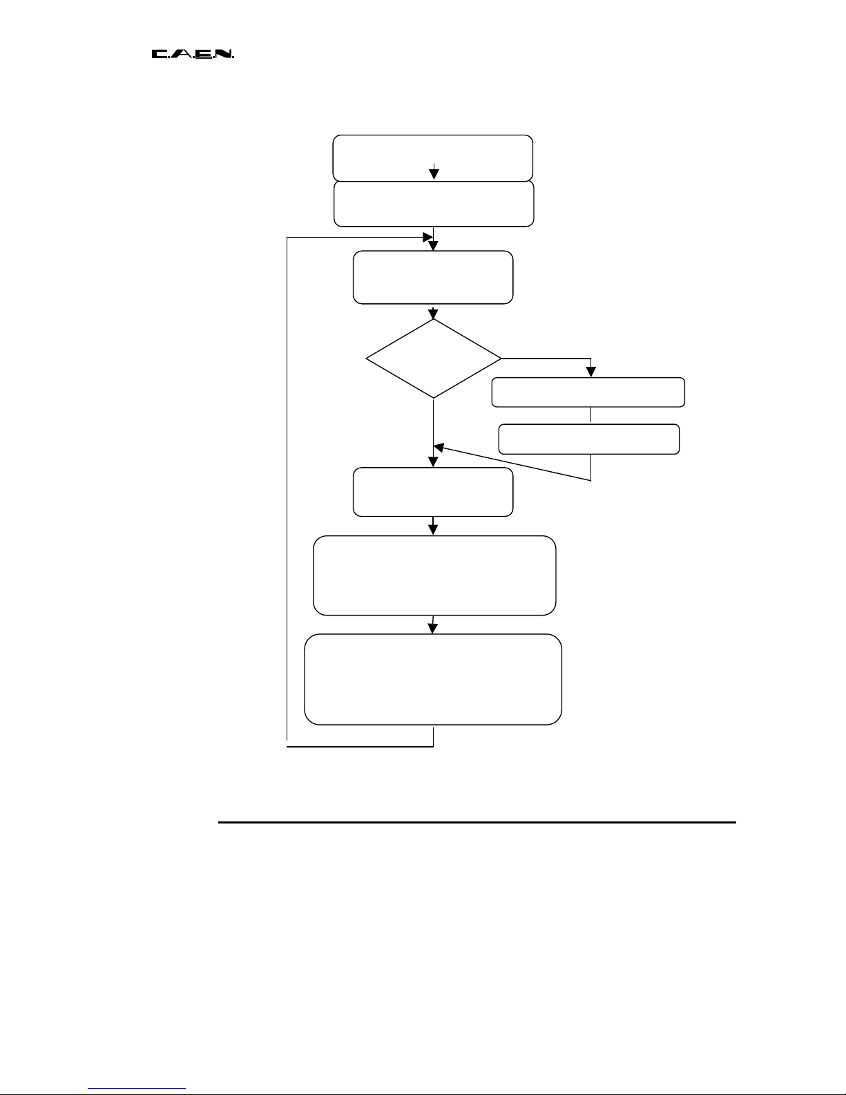
Fig 2.4 shows the standard course of an acquisition :
The sequence begins with the initialization of the board by a RESET order.
Next, the different parameters which are not used with their default value must be
programmed (PRETRIG, POSTTRIG, TRIGGER TYPE, TRIGGER EDGE, MASK, NB
OF COL TO READ, FP FREQUENCY, …).
The starting order of the acquisition is next sent.
Page 11

PRELIMINARY
Document type: Title: Revision date: Revision:
User's Manual (MUT) Mod. V1729 4 Channel 12 Bit Sampling ADC 22/06/2005 3
NPO: Filename: Number of pages: Page:
00109/04:V1729.MUTx/03 V1729_REV3.DOC 38 11
The user if necessary sends a software trigger (in the case of an automatic trigger)
having taken care to wait at least the time necessary for the PRETRIG.
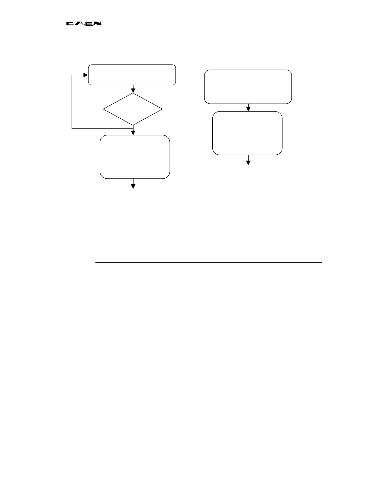
- The program then waits for a request emitted by the V1729 board when the data are
ready to be read. For this, there exist two possibilities illustrated by Fig 2.5 :
Waiting and handling of an interruption (SRQ in GPIB, IRQ3 in VME).
Regular scanning of the LSB of the interruption register (INTERRUPT h80).
In both cases, the user should acknowledge the request by writing a 0 in the
INTERRUPT register, but the latter is anyhow reset by the START_ACQ command. The
first solution has the big advantage of being less noisy for the front-end of the board.
- The user can then partially or wholly read the data stored in the board. This includes :
the values of the vernier and of the samples (see 4.7 )
the value of TRIG_REC which permits determination of the position of the trigger in the
acquisition window (see 2.5.2)
- The user must correct the data before using it (see 2.5):
By subtracting the pedestals (see 2.1.1).
By reordering the data (see 2.5.2).
These operations can be executed on-line or off-line according to the context.
2.5 Correction of data
The raw data extracted from the board must be treated before really being usable.
This treatment consists of two operations :
Correction of the pedestals.
Reordering and time alignment of the data.
Page 12
PRELIMINARY
Document type: Title: Revision date: Revision:
User's Manual (MUT) Mod. V1729 4 Channel 12 Bit Sampling ADC 22/06/2005 3
NPO: Filename: Number of pages: Page:
00109/04:V1729.MUTx/03 V1729_REV3.DOC 38 12
Fig. 2.5: block diagram of a standard acquisition
2.5.1 Correction of the pedestals
The analog memories of the MATACQ chips present by design dispersions of pedestal
from cell to cell which can reach several tens of mV. On the other hand, the pedestal of a
data cell is extremely reproducible (250µV RMS). Due to the structure of the chip, the
dispersion of the pedestals presents a principal periodicity of 20 cells, followed by a tiny
individual distribution. If not compensated, this dispersion will appear as a noise at the
reconstruction of the signal because of the random position of the trigger in the matrix.
Board Parameters Initialization
Send START
A
CQUISITION
Wait for REQUEST
Trigger
auto ?
Send SOFT TRIGGER
yes
no
Read Data:
• Read verniers & samples.
• Read TRIG_REC
Correct & Reorder Data:
• Subtract pedestals.
• Reorder data & calculate times
next acquisition
Send RESET BOARD
Wait for end of PRETRIG
Page 13
PRELIMINARY
Document type: Title: Revision date: Revision:
User's Manual (MUT) Mod. V1729 4 Channel 12 Bit Sampling ADC 22/06/2005 3
NPO: Filename: Number of pages: Page:
00109/04:V1729.MUTx/03 V1729_REV3.DOC 38 13
Fig. 2.6: two possibilities for detection and for treatment of the request
In order to obtain the nominal noise performances (signal to noise ratio of 73 to 74dB),
the pedestals, which are stable in time and with temperature, must be removed by the
acquisition software individually cell by cell. Since the pedestal of a cell is linked to its
physical location and not to its position in relation to the Trigger, it is necessary to
realize this removal BEFORE reordering the data.
A method of calibration of the pedestals is demonstrated in section 3.3.2.
2.5.2 Temporal corrections
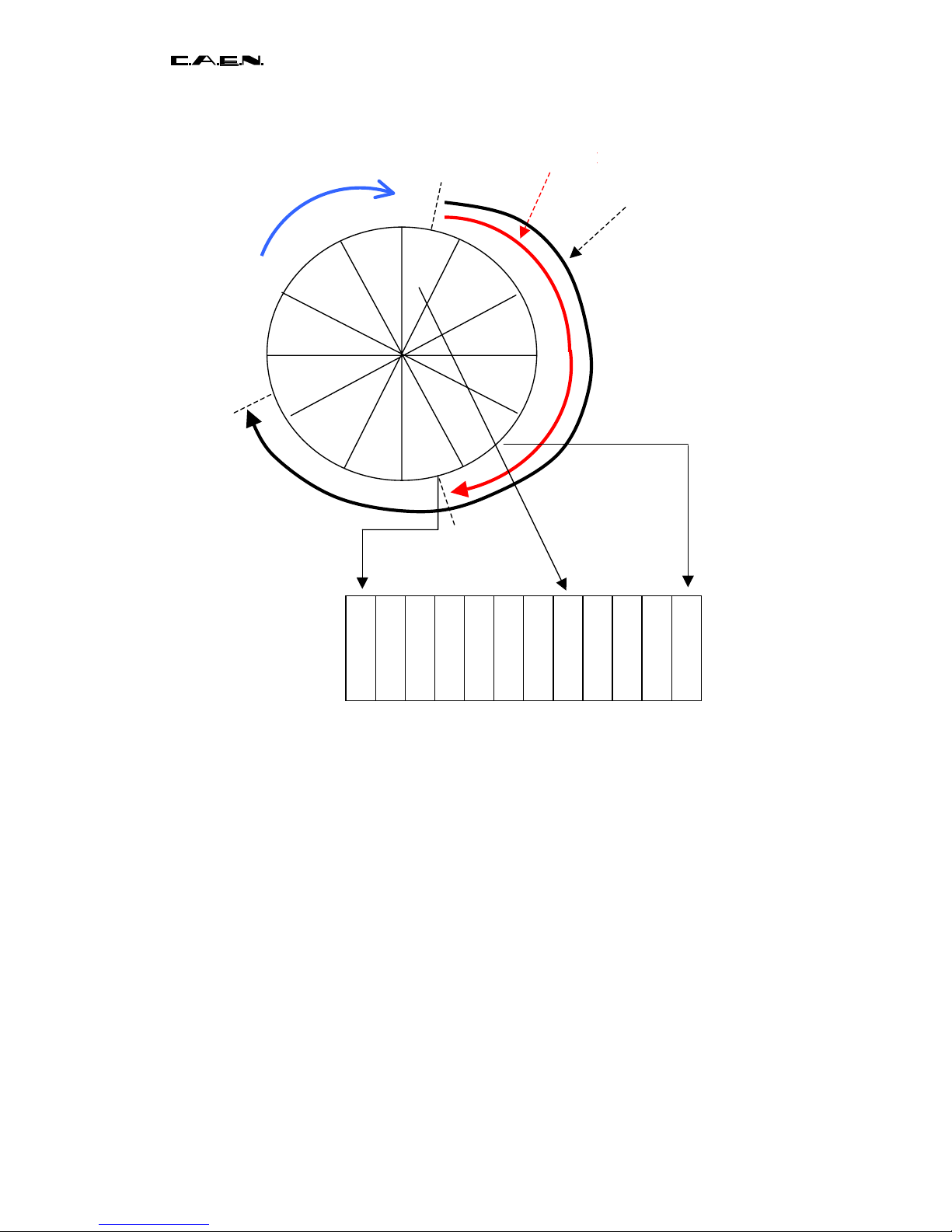
The signal is sampled in a circular memory. The first operation necessary for the
treatment of the data is therefore to « unfold » the circular memory in order to obtain a
table of 2560 temporally ordered data (see Fig 2.6). This can be done, by example, by
realizing a rotation of :
ROT = (TRIG_REC - POSTTRIG ) * 20
cells towards the left of the data table issued from the RAM.
Or, equivalently through a calculation of a new index number for each data :
(2) NEWi = (2560 + OLDi – END_CELL) modulo 2560
where END_CELL is the index of the last written cell :
END_CELL = 20 * (POSTTRIG + TRIG_REC) modulo128
The trigger signal (asynchronous trigger) Ta is the absolute reference which serves to
temporally realign the data. In order to find its position, one uses the information provided
by a temporal interpolator (vernier) measuring ti, time interval separating the arrival of Ta
from the next rising edge of the Fp clock.
Interrupt request
acknowledge => clear
INTERRUPT
REGISTER
Bit 0 =1
?
yes
Read INTERRUPT REGISTER
no
Interrupt request
acknowledge => clear
INTERRUPT
REGISTER
continue
Asynchronous Interrupt detected
by hardware (IRQ3 or SRQ)
Page 14
PRELIMINARY
Document type: Title: Revision date: Revision:
User's Manual (MUT) Mod. V1729 4 Channel 12 Bit Sampling ADC 22/06/2005 3
NPO: Filename: Number of pages: Page:
00109/04:V1729.MUTx/03 V1729_REV3.DOC 38 14
Fig. 2.7: unfolding of the circular memory
This information associated with the MINVER and MAXVER calibration constants (see
3.3.1 permits determination of the position of the Trigger and therefore realignment of the
data with a precision in the region of 50ps RMS. This realignment is unnecessary if the
user simply desires to study the signal shape and in this case, the curve acquired will
present a jitter of a period of Fp. The information of the 4 verniers from the same board
being redundant in order to realize the temporal adjustement, it is therefore possible :
- to use solely the vernier from the channel 0.
- to use the vernier i for the channel i.
- to calculate the mean of the 4 verniers in order to refine the time precision.
The following formula permits determination of the time of each point of the reordered
table, with by convention a time origin (Time = 0) at the arrival of the Trigger.
(3) Time[NEWi] = DT0 + {NEWi - 20 *[128 - POSTTRIG + Correc_Ver]} * dT
With:
(4) Correc_Ver = (VERNIER - MINVER) / (MAXVER - MINVER)
Writing
direction
Last cell
=cell n
trigger
cell
n+1
cell
n+2
cell
127
cell 0
cell 1
cell i
cell n -1
cell …
cell …
1.1.1.1.1.1.1.1
P
1.1.1.1.1.1.1.
2
REORDERED
ARRAY
CIRCULAR
BUFFER
S
T
A
R
T
T
RIGEN
D
cell …
cell …
Page 15

PRELIMINARY
Document type: Title: Revision date: Revision:
User's Manual (MUT) Mod. V1729 4 Channel 12 Bit Sampling ADC 22/06/2005 3
NPO: Filename: Number of pages: Page:
00109/04:V1729.MUTx/03 V1729_REV3.DOC 38 15
Where:
dT is the sampling period (500ps or 1ns)
DT0 is a fixed temporal offset, close to 0, due to signal propagation times in the board (of
which the calibration is described in 3.1.1)
An alternative but equivalent solution, consists in generating the reordered table through
a rotation towards the left of the data of :
(1b) ROT = (TRIG_REC - POSTTRIG ) * 20 – INT(Correc_Ver*20) cells
where INT corresponds to rounding off to the nearest whole number.
The trigger is then situated at a time
(5) tT= [Correc_Ver*20– INT(Correc_Ver*20)]* dT
before the cell numbered 20*(128-POSTTRIG) (plus the offset DT0).
Page 16

PRELIMINARY
Document type: Title: Revision date: Revision:
User's Manual (MUT) Mod. V1729 4 Channel 12 Bit Sampling ADC 22/06/2005 3
NPO: Filename: Number of pages: Page:
00109/04:V1729.MUTx/03 V1729_REV3.DOC 38 16
3. Synchronizations and calibrations
3.1 Synchronization between the channels
3.1.1 Channels from the same board
A single trigger signal is used for all of the channels from the same board. The
acquisition of these channels will therefore naturally be synchronous, with a typical jitter
of only 20ps RMS. The possible temporal offset dT0, constant, between the channels
(principally due to the propagation of the trigger signal on the board, but also to the
different lengths of cables at the inputs) will be calibrated once for all. This calibration is
executed by sending a same signal on all of the inputs and by looking for the fine position
of the trigger on each of the channels.
In the case where the board is triggered on one of the input signals, a fine
synchronisation method consists of interpolating by software the crossing of the signal
through the trigger threshold on the given channel, this permitting the fine datation of all
the measured channels.
3.1.2 Channels situated on different boards
The synchronization is only possible if the trigger source is common to the different
boards. For this, several possibilities can be envisaged :
- to use an external trigger signal common to all of the boards.
- to generate the trigger signal on a fixed board (master) which triggers itself and to send
its TRIG_OUT signal output to the external trigger input of the other boards (via a NIM
buffer if there is more than one target board).
- to generate the trigger signal on any one of the boards. The TRIG_OUT outputs of all of
the boards will then be connected on an external NIM logic then the result will be
redistributed in a synchronous fashion to all the boards via their EXT_TRIG input. It is
this latter input which will then be programmed as the source of the asynchronous trigger
via the bit 4 of the TRIGGER_TYPE register on all the boards.
In all cases a calibration of the temporal offset between the boards is necessary. This
calibration, similar to that which is necessary to align the channels from the same board,
will be dependent upon the set-up (length of the cables…).
3.2 SYNC_OUT and BUSY signals
One of the NIM outputs of the front panel can be configured either as a SYNC_OUT, or
as a BUSY respectively with the help of the S4 and S2 straps. SYNC_OUT is a
synchronization signal corresponding to the writing in the first cell of the second column
of the circular analog memory, and which can be made available on the front panel. For
certain applications, this signal can permit triggering of the source analog signals and
thus guaranties their fixed position in the memory. Thus, if the temporal occupation of the
signals to acquire is low, the user will have the possibility to only re-read the beginning of
the depth of the analog memory and to thus limit the dead time linked to the acquisition.
Page 17

PRELIMINARY
Document type: Title: Revision date: Revision:
User's Manual (MUT) Mod. V1729 4 Channel 12 Bit Sampling ADC 22/06/2005 3
NPO: Filename: Number of pages: Page:
00109/04:V1729.MUTx/03 V1729_REV3.DOC 38 17
BUSY is a signal destined to inform the external world that the board is not ready to
receive a signal (it is either idle, or in the process of transferring data between the
MATACQ chips and the RAM, or at the beginning of the acquisition phase). Its transition
to 0 indicates then that the board is now ready to record a signal.
3.3 Calibrations
In order to attain the optimal metrological performance, the V1729 board requires
calibrations. These remain valid for several weeks, even several months.
3.3.1 Calibration of the interpolator
The temporal interpolator (vernier) requires a calibration. This calibration, based on a
statistical measure, will require the acquisition of several thousand events and can last
from one second to a couple of minutes depending on the type of bus and on the
software used. It can be done with the inputs connected to any source, but the trigger
must be asynchronous in relation to the clock. The result of this calibration will be a
“square” histogram, of which the sides correspond to two successive rising edges of Fp.
The corresponding value on the left side (MINVER) will be the « zero » of the vernier,
and the one on the right side (MAXVER) will correspond to a vernier of 1/Fp (in other
words 10 or 20ns). The intermediate values will next be deduced at the time of the
acquisitions by a simple proportional calculation.
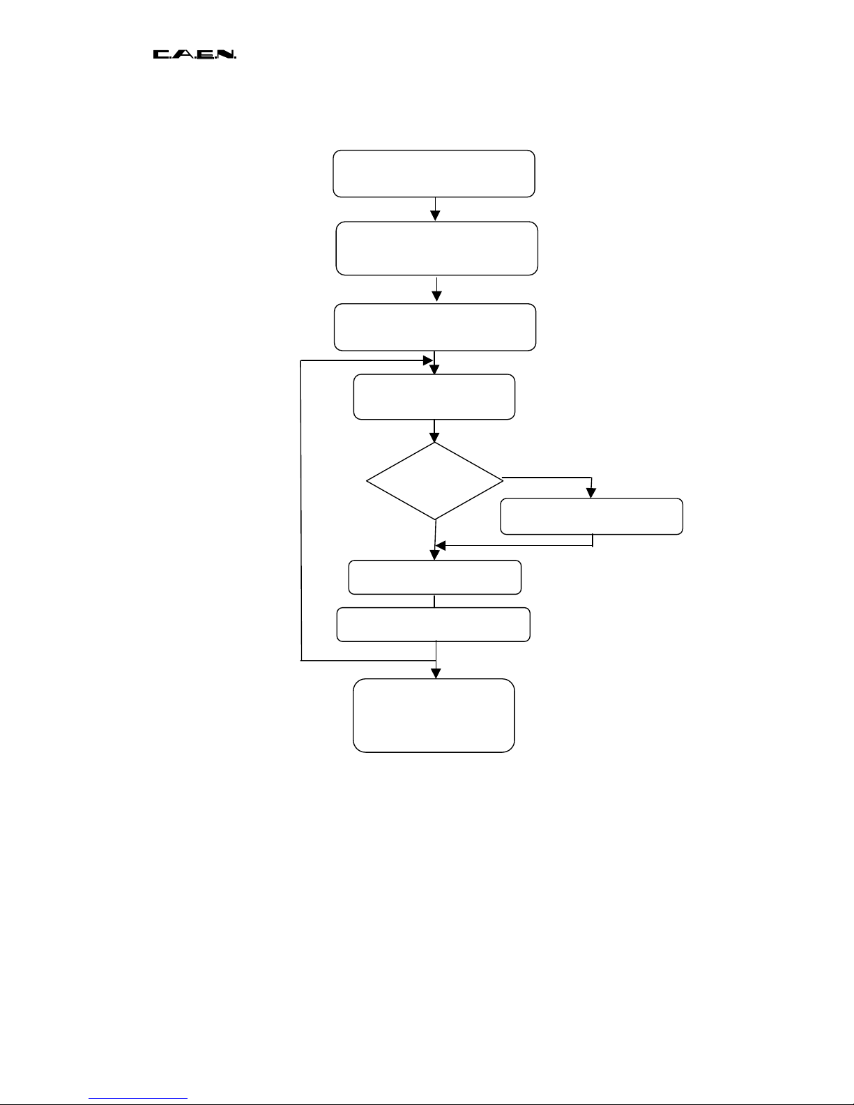
The diagram in Fig 3.1, which follows from that in Fig 2.5, shows the sequencing of such
a calibration. It is optimized so as to be the fastest possible. In particular :
The PRETRIG and POSTTRIG are fixed at their minimal value.
NB_OF_COL_TO_READ has to be set to 1.
Only the vernier values are read in the RAM. In other words, if NCH channels are read,
only the 2*NCH first data are read and only the NCH+1 to 2*NCH words are conserved
(see 4.7).
After a certain number of acquisitions (at least 10000), the boundaries of the vernier
MINVER and MAXVER can be calculated.
At first approximation, it is possible to simply use the minimal and maximal values of the
vernier for MAXVER and MINVER. This method is sufficient to obtain temporal
resolutions in the region of 70ps RMS.
To have greater precision, one must in order to find the two sides fix a threshold
corresponding to half the mean number of ADC counts in the « square » distribution.
To obtain even more precision, it is possible to use more complex methods.
A second, much faster method of calibration is available. For this :
Charge NB_OF_COL_TO_READ at 0.
Position the trigger in auto mode.
Authorize the internal random trigger.
Launch a Start_ACQUISITION.
Page 18
PRELIMINARY
Document type: Title: Revision date: Revision:
User's Manual (MUT) Mod. V1729 4 Channel 12 Bit Sampling ADC 22/06/2005 3
NPO: Filename: Number of pages: Page:
00109/04:V1729.MUTx/03 V1729_REV3.DOC 38 18
Fig. 3.1: diagram of the calibration of the verniers
The codes which implement the register setting is the following:
void TCAENADC::Vernier()
{
char s[30];
SetNCols(0);
// Setto PRETRIG
SetPreTrig(1);
// Setto POSTTRIG
SetPostTrig(1);
//??
SetTriggerType(0x08);
int i;
Set PRETRIG=POSTRIG=1
Send START
ACQUISITION
Trigger
auto ?
Send SOFT TRIGGER
yes
no
Read vernier data only
next acquisition
Send RESET BOARD
Board parameters initialization
Calculate MINVER &
MAXVER for each
channel
Wait for request
Page 19

PRELIMINARY
Document type: Title: Revision date: Revision:
User's Manual (MUT) Mod. V1729 4 Channel 12 Bit Sampling ADC 22/06/2005 3
NPO: Filename: Number of pages: Page:
00109/04:V1729.MUTx/03 V1729_REV3.DOC 38 19
StartAcq();
Wait();
GetVernier(vernier);
//fwrite(vernier,sizeof(vernier),1,Fvernier);
for (i=0;i<V1729_VERNIER_DEPH;i++){
sprintf(s,"%d\n",vernier[i]);
fwrite(s,1,strlen(s),Fvernier);}
printf("Vernier results saved\n");
}
void TCAENADC::GetVernier(unsigned short *vernier)
{
printf("TCAENADC::GetVernier()\n");
unsigned short buffer[V1729_VERNIER_DEPH];
int readed;
vme_adr = CAENBASEADDRESS + V1729_RAM_DATA_VME;
CAENVME_SetFIFOMode(Crate,1);
if (CAENVME_BLTReadCycle(Crate, vme_adr , (unsigned char*) buffer,
V1729_VERNIER_DEPH*2,cvA32_U_BLT,cvD32 , &readed )!= cvSuccess)
printf("TCAENADC::GetVernier() - Errore di Accesso\n");
CAENVME_SetFIFOMode(Crate,0);
for (int j = 0; j < V1729_VERNIER_DEPH; j++) vernier[j] = buffer[j] & 0xFFFF;
}
The RAM (buffer[i]) is then filled with 65536 vernier values corresponding to 16384
random triggers. For each trigger one finds only 4 values, arranged in the following
order :
Channel 3 vernier, channel 2 vernier, channel 1 vernier, channel 0 vernier.
It is then necessary to rearrange the buffer in order to obtain 4 arrays (one per channel)
of 16384 samples each.
With such settings we send on each channel a slope signal with 1/Fp duration in such a
way that, if we make an histogram of the channel data, we obtain a “square” signal,
whose edeges correspond (in time) to the Fp ramp-up fronts. The leftmost value
correspond to MINVER, the rightmost to MAXVER.
The result is similiar to a differential non linearity measure and is used in the calibration
in order to weigh the Venier single datum obatined during acquisition; this allows to
measure on which percentage of the clock period the time correction must be performed.
At the end of this calibration, an interruption is generated in order to permit the user to
launch a reading. This reading can be realized in block mode, which permits realization
of the calibration of the vernier in less than one second.
One must note that for this particular method of calibration, the distributions obtained are
not necessarily uniform. Nevertheless, the MAXVER and MINVER boundaries are
extremely well-defined and therefore perfectly exploitable for corrections.
Our experience showed us that this calibration remains valid several weeks, even
several months.
Page 20

PRELIMINARY
Document type: Title: Revision date: Revision:
User's Manual (MUT) Mod. V1729 4 Channel 12 Bit Sampling ADC 22/06/2005 3
NPO: Filename: Number of pages: Page:
00109/04:V1729.MUTx/03 V1729_REV3.DOC 38 20
3.3.2 Calibration of the pedestals
For this, a calibration of the baselines is necessary. This operation will be necessary
following all changes either in the frequency of sampling, or in the bandwidth of the write
amplifier (BWL), or in the read modes (FAST READ MODES). It will consist in realizing a
mean measurement over a few tens of raw acquisitions of the baselines for all of the
cells (disconnected or grounded inputs). The trigger must then be either automatic, or
external.
The acquisition procedure is the same as for a standard acquisition, but the reading of
TRIG_REC can nevertheless be skipped. Of course not the least temporal correction is
made on the data. At each acquisition, the table of the means will be computed and
finally recorded for an eventual subtraction by software from the unaligned raw data. This
calibration operation lasts less than one second.
In cases where the input is connected to unlikely physical signals, it is also possible to
realize this calibration without disconnecting the input. However, it will then probably be
necessary to increase the number of acquisitions in order to diminish the effect of the
induced additional noise.
Our experience shows us that this calibration remains valid several weeks.
3.3.3 Temporal calibration between different channels
See 3.1
Page 21

PRELIMINARY
Document type: Title: Revision date: Revision:
User's Manual (MUT) Mod. V1729 4 Channel 12 Bit Sampling ADC 22/06/2005 3
NPO: Filename: Number of pages: Page:
00109/04:V1729.MUTx/03 V1729_REV3.DOC 38 21
4. Technical specifications
4.1 Packaging
The Model V1729 is housed in a one unit standard VME unit.
4.2 Sampling frequency
The V1729 board is sequenced by an oscillator at Fp frequency. No greater frequency
signal exists on the board. This is what explains the low consumption of the system. The
sampling at a very high frequency (Fe) in the MATACQ chip is in fact realized by virtual
multiplication of frequency inside the chip by a factor up to 20.
The MATACQ chip functions with Fp = 50MHz or 100MHz programmable on the board
by software, which corresponds to a sampling frequency Fe (= 20*Fp) of 1 or 2 GHz.
4.3 Input signals, Dynamic range
The V1729 board integrates 4 analog channels. The inputs of these channels are
connected through double LEMO plugs (IN0+/- à IN3+/-).
The inputs are by default unipolar and terminated on 50 Ohms. However, the input levels
of the board can be very easily modified (through displacing a few resistors and mounting
new ones) in such a way as to permit the input in differential mode (from which the
double LEMO plugs). For this purpose, free CMS-805 resistor footprints are indeed
implemented on the V1729 board (see IV.1.g).
The analog to digital conversion is made on 12 bits with a maximum dynamic range of
1V, or an LSB of 250µV. This range is centered on 0V (+/- 0.5V).
The measured noise referred to input is less than 200 µV RMS (i-e below the lsb of the
ADC), and the non-linearity remains below 1 per 1000 over the whole dynamic range.
Page 22
PRELIMINARY
Document type: Title: Revision date: Revision:
User's Manual (MUT) Mod. V1729 4 Channel 12 Bit Sampling ADC 22/06/2005 3
NPO: Filename: Number of pages: Page:
00109/04:V1729.MUTx/03 V1729_REV3.DOC 38 22
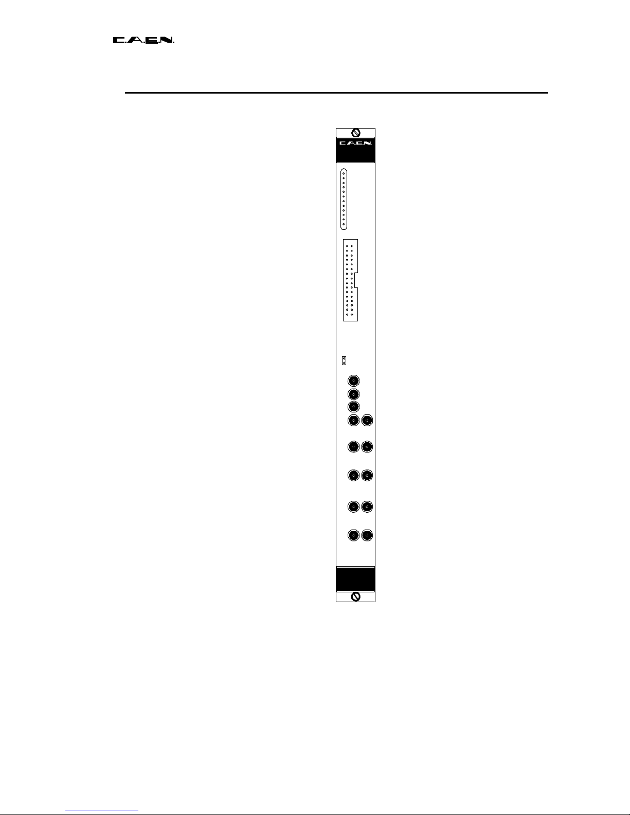
4.4 Front panel
Mod. V1729
4 CH-12 BIT
VCC
EXT
CLK
ADC
+8 TO 12 V
-8 TO 12 V
VME
GPIB
RESET
CLOCK
BUSY
ACQRUNNING
TRI G
WR-RAM
INTERRUPT
GPIB
EXT
DIFF
TRG
+
-
TRG
OUT
BUSY/
SYNC
OUT
EXT
TRG
EXT
EN
TRG
IN0+ IN0-
IN1+ IN1-
IN2+ IN2-
IN3+ IN3-
Fig. 4.1: Mod. V1729 Front Panel
Page 23
PRELIMINARY
Document type: Title: Revision date: Revision:
User's Manual (MUT) Mod. V1729 4 Channel 12 Bit Sampling ADC 22/06/2005 3
NPO: Filename: Number of pages: Page:
00109/04:V1729.MUTx/03 V1729_REV3.DOC 38 23
4.5 Mechanical and electrical standards
4.5.1 Mechanical standard
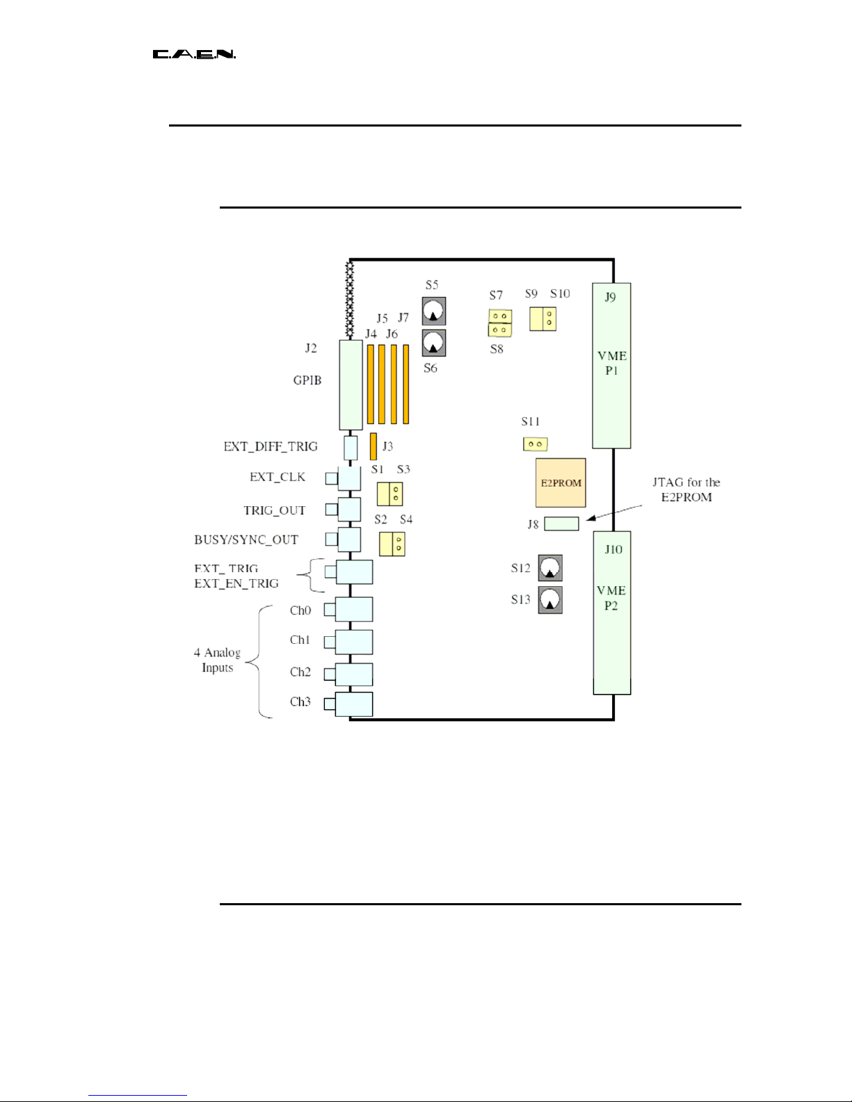
Fig. 4.2: implementation of the connectors and configuration elements on the V1729
The V1729 board is of VME 6U mechanical format. The two connectors P1 and P2 of the
VME crate are usable, both for the supply and the VME dialogue. However, these boards
can completely be accessed via the GPIB bus out of a VME crate, or by only using the
latter as mechanical and power supply support.
The plugs used for all the digital inputs/outputs are of female LEMO type. The analog
inputs are in double LEMO.
4.5.2 Electrical interfaces
The V1729 board is compatible with two acquisition buses :
Page 24
PRELIMINARY
Document type: Title: Revision date: Revision:
User's Manual (MUT) Mod. V1729 4 Channel 12 Bit Sampling ADC 22/06/2005 3
NPO: Filename: Number of pages: Page:
00109/04:V1729.MUTx/03 V1729_REV3.DOC 38 24
- VME via the P1 connector of the VME (plus the P2 for the A32/D32 mode), 96 pin male
connector DIN 41612 .
- GPIB via the HE10 connector located on the front panel (26 points male).
This board has an address coded over 8 or 16 bits, configurable through a set of
hexadecimal rotary switches. For the GPIB and the VME A24/D16, one uses only the two
rotary switches S5 and S6. For the VME A32/D32, one must also use the two rotary
switches S10 and S11.
In GPIB, the address is configurable from 1 to 29 (decimal).
In VME, the address is configurable from h01 to hFF on the bits 16 to 23 for the A24/D16
mode, and from h0001 to hFFFF on the bits 16 to 31 for the A32/D32 mode.
The choice of the type of interface is determined by the S9 jumper. By default (without
jumper), the bus used is the VME. When the jumper is mounted, it is the GPIB which is
used.
4.5.3 Summary of front panel signals
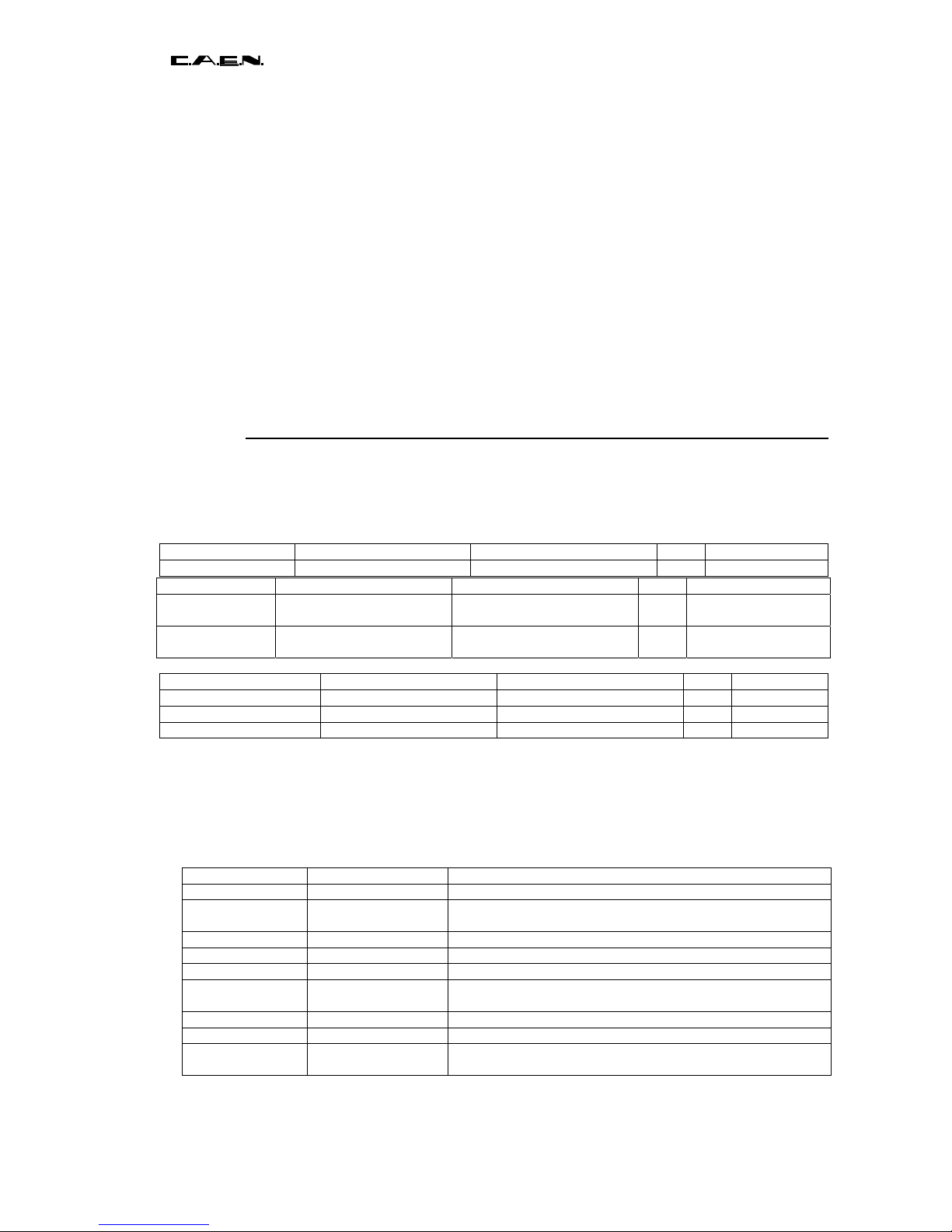
The fast logical signals of input “EXT_TRIG” and of output “BUSY/SYNC_OUT” and
“TRIG_OUT” of the V1729 board use the NIM standard (-16mA in 50 Ohms for the
logical state « 1 », no current for the logical state « 0 »).
EXT_EN_TRIG External Trigger Enable Half double LEMO I NIM
EXT_TRIG External Trigger Half double LEMO I NIM
EXT_DIFF_TRIG External Trigger Double pin I DIFF ECL
EXT_CLK External clock LEMO I NIM
TRIG_OUT Trigger Output LEMO O NIM
BUSY/SYNC_OUT Busy/Synchro Output LEMO O NIM
The front panel leds permit having an image of the current status of the board. The green
ones shows the presence of the external power supplies ; the yellow ones that of the
supplies realized on the board by the regulators. Finally, the red ones are linked to the
internal signals via monostables which permit the visualization of very short pulses and to
digital gates for the continuous levels.
Name Type Function
VME Monostable + gate VME access acknowledged by the board.
GPIB Monostable + gate GPIB access acknowledged. Remains ON if no EOI is sent by the
controller at the end of a writing sequence.
SPECS Monostable + gate SPECS access acknowledged.
RESET Monostable + gate Board reset.
CLOCK Monostable only The Altera FPGA is providing the main clock to the board.
ACQRUNNING Monostable + gate Is set ON after a “start acquisition” command. Is set OFF at the end of
the POSTTRIG.
TRIG Monostable + gate Image of the TRIGA signal.
WR-RAM Monostable + gate Write access to the data RAM.
INTERRUPT Monostable + gate Displays the INTERRUPT signal which is produced at the end of the
acquisition sequence.
Name Purpose Connector I/O TYPE
IN0+ to
IN3 +
Positive Analog Inputs Half double LEMO
or SMA
I 50Ohm terminated
IN0- to
IN3 -
Negative
Analog Inputs (option)
Half double LEMO I 50Ohm terminated
Page 25
PRELIMINARY
Document type: Title: Revision date: Revision:
User's Manual (MUT) Mod. V1729 4 Channel 12 Bit Sampling ADC 22/06/2005 3
NPO: Filename: Number of pages: Page:
00109/04:V1729.MUTx/03 V1729_REV3.DOC 38 25
4.5.4 Supplies
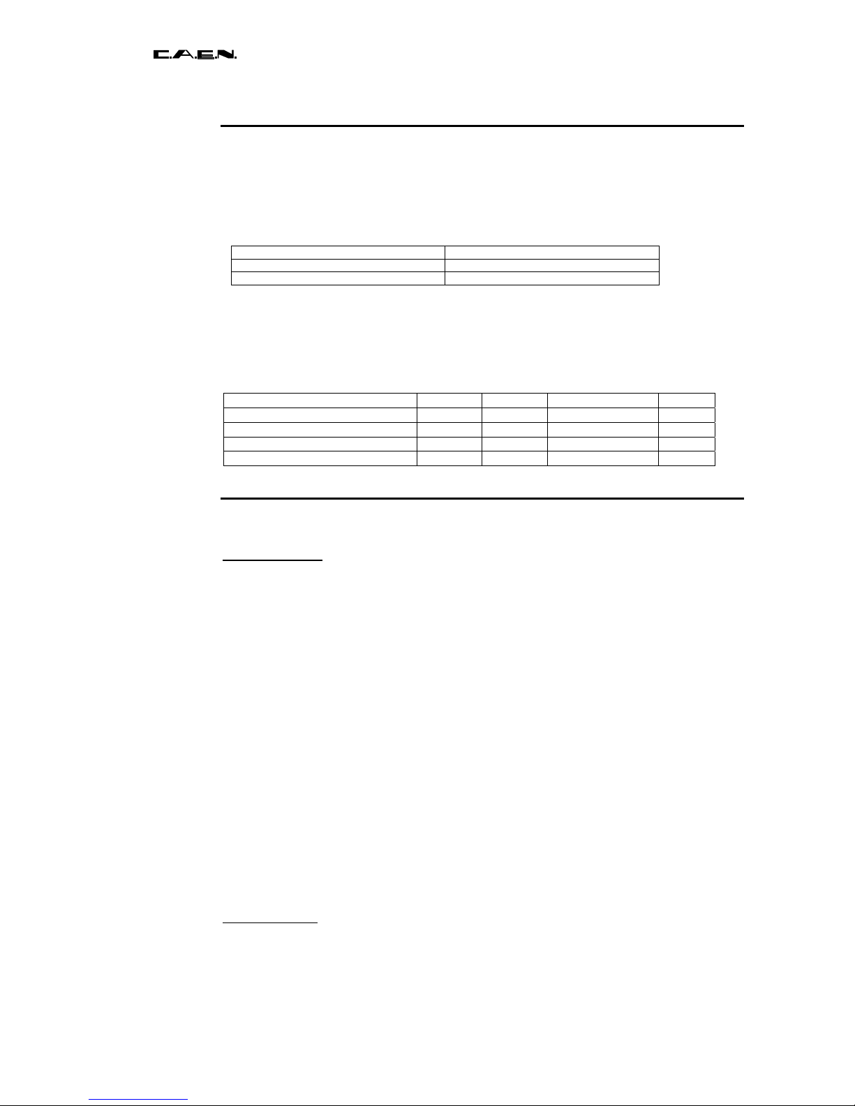
The V1729 board uses the standard supplies of the VME : +/-12V and +5V.
It fabricates the –5V for the ECL logics starting from the +5V with the help of a DCDC converter capable of delivering 600mA.
The intensities consumed on these different supplies are :
+12 V
0.3A + X x Y x 0.7A
-12V
0.2A + X x Y x 0.7A
+5V
1.5A
where X is the rate of acquisition = relation of time spent awaiting the event / total time .
X is worth 1 in the case of infrequent event acquistions.
X is low (can fall to 1%) in the case of frequent events. In this case indeed, the dead time
for readout is dominant in relation to the time spent awaiting the event.
Y depends on the bandwidth mode:
4.5.5 Pinout of the non-standard connectors
GPIB Connector (HE10 26 points male)
Reference : J2.
1 : D1 2 : D5
3 : D2 4 : D6
5 : D3 6 : D7
7 : D4 8 : D8
9 : EOI 10 : REN
11 : DAV 12 : GND
13 : NRFD 14 : GND
15 : NDAC 16 : GND
17 : IFC 18 : GND
19 : SRQ 20 : GND
21 : ATN 22 : GND
23 : GND 24 : GND
25 : NC 26 : NC
The corresponding HE10 female connector can be directly pressed on a 24 wire flat
cable equipped at the other extremity with a GPIB standard connector (CENTRONICS 24
points). Up to 18 HE10 female connectors can be mounted in parallel on the flat cable
(be careful then to only mount the bus polarization networks on only one of the boards).
JTAG connector
(HE10 10 pins male)
Reference : J8.
Permits the reconfiguration of the E2PROM (EPC2) from an Altera file « .pof » thanks to
JTAG.
BWL0 BWL1 Bandwidth Y
Full bandwidth mode
0 0 300 MHz 1
Normal mode
1 0 230 MHz 0,6
Normal mode
0 1 230 MHz 0,6
Low power mode
1 1 180 MHz 0,35
Page 26
PRELIMINARY
Document type: Title: Revision date: Revision:
User's Manual (MUT) Mod. V1729 4 Channel 12 Bit Sampling ADC 22/06/2005 3
NPO: Filename: Number of pages: Page:
00109/04:V1729.MUTx/03 V1729_REV3.DOC 38 26
4.5.6 Straps and resistor network sockets
A certain number of sockets for straps and resistor networks are available on the board.
These are their respective roles:
Reference Role
S1 one utilizes the differential EXT_TRIG differential input (exclusive of S3)
S3 one utilizes the unipolar EXT_TRIG input by Lemo (exclusive of S1)
S2 the BUSY/SYNC_OUT output releases the BUSY signal (exclusive of S4)
S4 the BUSY/SYNC_OUT output releases the SYNC_OUT signal (exclusive of S2)
S5 and S6 address of the board
S7
one utilizes the EXT_CLK input for the main clock (exclusive of S8)
S8
one utilizes the 100MHz oscillator for the main clock (exclusive of S7)
S9
Do not use
S10
choice of the acquisition data bus
S11
normally absent. Prevents the conf_done to rise which then permits not to
validate the configuration of the Altera at power-up.
S12 and
S13
address of the board
J3 adaptation for the EXT_DIFF_TRIG input. Place 100 ohms between the pins 1 and 2
and between the pins 3 and 4
J4 pull-down for the GPIB. Place an 8 resistor network 6.8k with common pin
J5 pull-up for the GPIB. Place an 8 resistor network 3.3k with common pin
J6 pull-down for the GPIB. Place an 8 resistor network 6.8k with common pin
J7 pull-up for the GPIB. Place an 8 resistor network 3.3k with common pin.
Caution : only place these 4 networks once if the boards are linked.
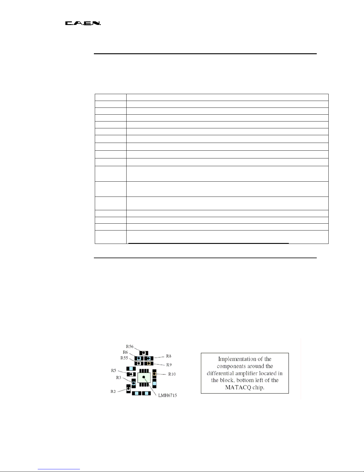
4.5.7 Implementation of differential inputs
The input signals are by default unipolar. In order to use differential inputs, one must
make use of certain free CMS-805 resistor locations located close to the input amplifiers
(LMH6715) and change some others. The equipment map of this zone of the board is
presented below. The already present resistors appear in blue, whereas the free
locations appear in white.
In order to wire a differential input (with both inputs adapted on 50 ohms), one must first
remove the resistors R3, R6 and R8. Then one has to put 84.5 ohms on R2, 0 ohm on
R5 (use the former R3), 121 ohms on R55 and 50 ohms on R56. Finally, R9 (750 ohms)
has to be replaced by 237 ohms and R10 (30.9 ohms) by 10 ohms.
Page 27
PRELIMINARY
Document type: Title: Revision date: Revision:
User's Manual (MUT) Mod. V1729 4 Channel 12 Bit Sampling ADC 22/06/2005 3
NPO: Filename: Number of pages: Page:
00109/04:V1729.MUTx/03 V1729_REV3.DOC 38 27
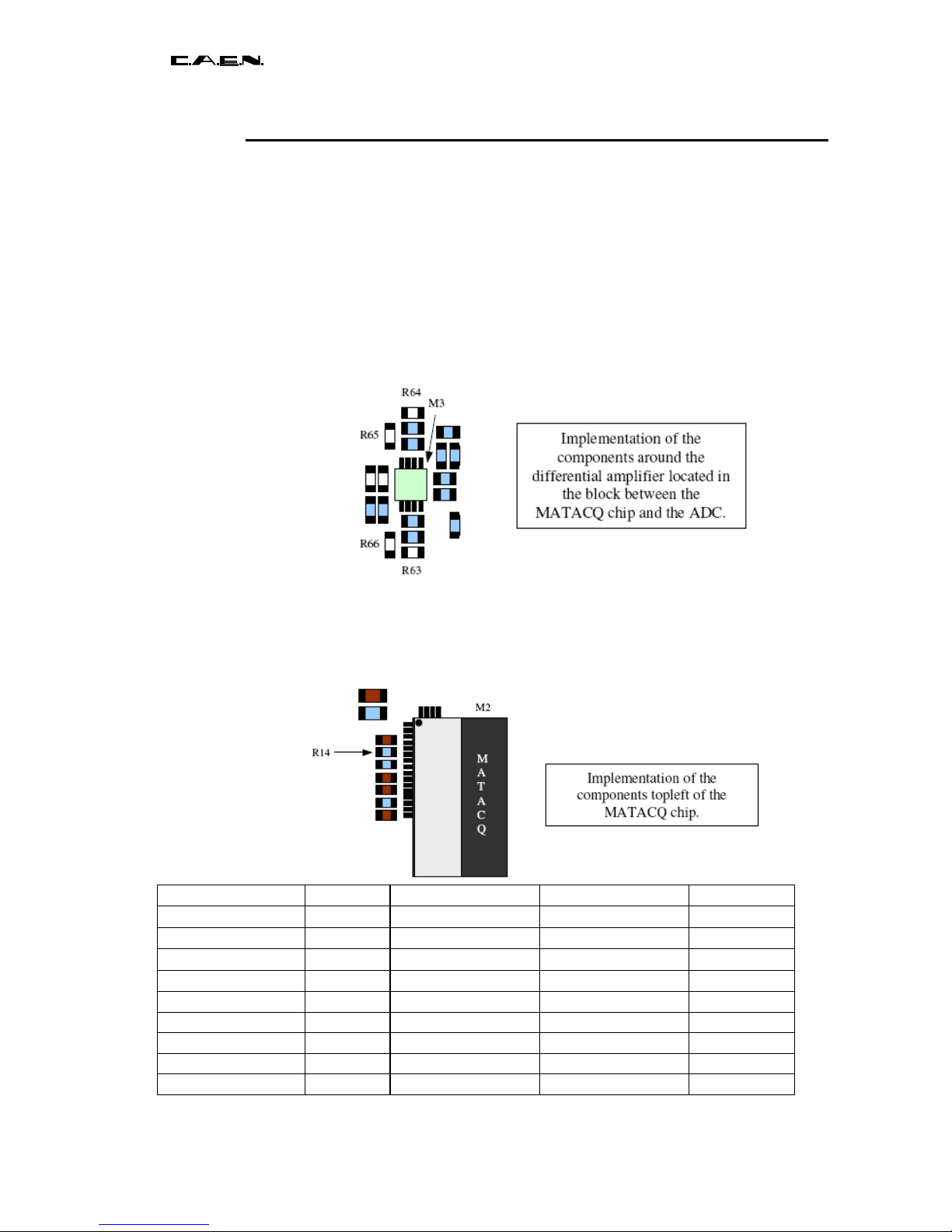
4.5.8 Using a shifted input range
The input signal range is defined by default to be +/-0.5V. In order to shift it, one has to
make use of free CMS-805 foot-prints located around the M3 amplifier (LM4130), itself
located between the MATACQ chip and the ADC (ADS803E). The equipment map of this
zone of the board is shown below.
To shift the baseline downwards in order to deal with mainly negative pulses, mount R64
and R66.
To shift the baseline upwards in order to deal with mainly positive pulses, mount R63 and
R65.
The values of those two 1%-precision resistors must be identical. The range is saturated
with 2k: that is therefore the minimum value. The tabulation below displays the different
resistor values necessary to obtain the targeted shifts.
It is also necessary to shift the fixed reference of the vernier (VerRef2) in order to
compensate for the preceding operation at the level of the latter. Therefore, one has to
modify the value of the resistor R14 (see figure below) which is 18k by default. It realizes
a dividing bridge with R15 (20k) located just below. One has actually to shift the middle of
that bridge with a voltage proportional to the shift aimed at on the signal itself. The values
necessary for R14 thus also appear in the tabulation below.
Input range pos -neg Shift in V Value of R63 & R65 Value of R64 & R66 Value of R14
90% -10% -0,4V 2,5k X 3,6k
80% -20% -0,3V 3,3k X 6k
70% -30% -0,2V 4,6k X 9k
60% -40% -0,1V 7k X 13k
50% -50% 0V X X 18k
40% -60% +0,1V X 7k 25k
30% -70% +0,2V X 4,6k 35k
20% -80% +0,3V X 3,3k 50k
10% -90% +0,4V X 2,5k 77k
Page 28

PRELIMINARY
Document type: Title: Revision date: Revision:
User's Manual (MUT) Mod. V1729 4 Channel 12 Bit Sampling ADC 22/06/2005 3
NPO: Filename: Number of pages: Page:
00109/04:V1729.MUTx/03 V1729_REV3.DOC 38 28
4.6 Interfaces
4.6.1 VME interface
The board is compatible with the A24-D16 and A32-D32 modes. It supports the h09,
h0B, h0D, h0F, h39, h3B, h3D and h3F ADDRESS MODIFIERS, and therefore deals
with the accesses in block mode.
The base address is given by : switch_address x h10000 (0<switch_address<hFF
for A24-D16 and 0<switch_address<hFFFF for A32-D32)
The offset is given by: sub_address x h100
The complete address is given by : base_address + offset
The IRQ3 is used to signal to the acquisition system the presence of data waiting in the
RAM. This interruption should be released by any writing at the address of the
INTERRUPT register, which sets it back to 0. It is anyhow also reset by the START_ACQ
command.
The sending of IRQ3 can be inhibited by the positioning at 1 of the INH_IRQ bit (bit 1 of
the CONTROL_REG register).
The presence of waiting data can be equally detected without treating the interruption,
but by scanning the presence of a 1 in the same INTERRUPT register. However, it
should be avoided because it is a source of noise during the data acquisition.
The reading of the data stored in the RAM is executed by realizing N successive
readings at the address of RAM_DATA or by realizing series of readings in block mode
at this same address (blocks of 128 16-bit words or 64 32-bit words maximum to comply
with the VME standard).
4.6.2 GPIB Interface
The V1729 boards can have an address set between 0 and 29 (decimal).
Writing
The GPIB commands are carried out by writing a string of characters in the board
situated at the address designated by the rotary switches.
The ASCII code of the first character corresponds to the sub-address of the order to be
executed or of the register to be addressed.
The ASCII codes of the following characters correspond to the data (only one data byte
except in the case of a writing to the sub-address hFF).
Reading
A method of reading by block was implemented to accelerate the reading by GPIB. The
reading of an element is thus executed in the following way :
* Writing operation of the 4 characters (#FF)(#LSB)(#MSB)(#REG) with
(#FF) : ASCII hFF code character
(#LSB) : ASCII code character corresponding to the 8 lowest significant bits of the
number of bytes to read (nbyte).
(#MSB) : ASCII code character corresponding to the 8 most significant bits of the number
of bytes to read.
Page 29

PRELIMINARY
Document type: Title: Revision date: Revision:
User's Manual (MUT) Mod. V1729 4 Channel 12 Bit Sampling ADC 22/06/2005 3
NPO: Filename: Number of pages: Page:
00109/04:V1729.MUTx/03 V1729_REV3.DOC 38 29
(#REG) : ASCII code character corresponding to the sub-address of the register to read
(h0C to read the data stored in the RAM for instance).
* Reading operation of nbyte characters.
In the general case (outside DATA RAM) nbyte =1.
In GPIB, the 16 bits of data converted by the ADC are read in two consecutive bytes in
the order MSByte, LSByte.
Interruption
At the end of the emptying of the data in the RAM, the V1729 board generates a
« Service Request (SRQ)» on the GPIB bus. The board is not compatible with the
PARALLEL or SERIAL POLLING protocols. However the GPIB controller can identify the
SRQ emitor by sequentially scanning the INTERRUPT registers of the different boards. It
is not a source of noise because the acquisition is then already terminated.
Like in VME, the interruption (SRQ) is set back to 0 by any writing at the address of the
INTERRUPT register, or by the START_ACQ command. In the same way, the presence
of waiting data can equally be detected without treating the interruption, but by scanning
the presence of a 1 in the same INTERRUPT register.
Broadcast Mode.
A writing at the address 30 (decimal) permits realization of a writing in all the V1729
boards present on the GPIB bus.
4.7 Reading of the data in the RAM, mapping
During the reading of the MATACQ chips, the data are digitized by the 12-bit ADC then
transferred in the RAM. The sequence order is always the same : one starts by reading
the first cell (upper left-hand) of the matrix, and one finishes with the last one (lower righthand), this independently of the position of the trigger and of the stopping point of the
acquisition.
One will therefore have to realign the data in relation to the trigger, which was explained
in 2.5.2. The channels are treated in parallel, and can be masked individually during the
writing in RAM. This implicates that, in the case where NCH channels are validated by
the mask (default value = h0F), the data are organized in 16-bit words by groups of NCH
addresses corresponding to the NCH channels (in the order 3 to 0, minus the masked
channels). The table below clarifies the arrangement of the words in the RAM (10252
words maximum).
The data in the table marked with an asterisk (*) are reserved for expert usage.
RAM internal address (HEX) Type of data
0000 to NCH-1
First sample (*)
NCH to 2*(NCH)-1
Vernier
2*NCH to 3*(NCH)-1
Reset baseline (*)
3*NCH to 4*(NCH)-1
1st cell
4*NCH to 5*(NCH)-1
2
nd
cell
5*NCH to 6*(NCH)-1
3
rd
cell
…
…
2562*NCH to 2563*(NCH)-1
2559th cell
2563*NCH to 2564*(NCH)-1
2560th cell (last cell)
Page 30

PRELIMINARY
Document type: Title: Revision date: Revision:
User's Manual (MUT) Mod. V1729 4 Channel 12 Bit Sampling ADC 22/06/2005 3
NPO: Filename: Number of pages: Page:
00109/04:V1729.MUTx/03 V1729_REV3.DOC 38 30
If the number of columns to read (register NB OF COLS TO READ) chosen is less than
128 (default value), the transfer in RAM will stop as soon as this number has been
reached. In such a case, one must be sure that the useful data is located in the first part
of the matrix. This is the role of the SYNC_OUT output which signals the passage into
the beginning of the matrix. In order to validate it, the ESO bit must be placed at 1 in the
control register and one must displace the corresponding strap (S2).
The channel mask register furthermore permits validation of only the utilized channels,
which will also permit reduction of the volume of data stored in the RAM. In this case
indeed, only the data of the valid channels will be recopied in the RAM, all the while
respecting the same storage order of the data.
The access to reading in the RAM is done by secondary addressing. Its internal address
is indeed controlled by a 16-bit counter (RAM_INT_ADD) located in the controller placed
on the board in the FPGA. This is not to be managed by the external interfaces, the
acquisition sequencer generating its own address starting from zero for the writing in the
RAM. This counter gets auto-incremented in the course of the addressing. It is
systematically reset at zero at the end of the writing cycle, which permits not having to
load it when one wants to read all of the memory. However, one can directly have access
to an address or a group of addresses given in the RAM by pre-loading it.
Seen from the bus, the reading in the RAM is therefore always done at the same h0C (in
GPIB) or h0D (in VME) address.
In GPIB, the 13 bits of data converted by the ADC and stored in the RAM (accessible by
reading of 2 bytes at the 0C address) are read in order MSByte, LSByte. Only the 13
LSbits of the data issued from a conversion of the ADC have a significance : the bits from
0 to 11 correspond to the 12 encoded bits. The bit 12 is at 1 in cases of overflow. The 3
MSbits are fixed at 0 on the board, they can be masked at the reading.
Page 31
PRELIMINARY
Document type: Title: Revision date: Revision:
User's Manual (MUT) Mod. V1729 4 Channel 12 Bit Sampling ADC 22/06/2005 3
NPO: Filename: Number of pages: Page:
00109/04:V1729.MUTx/03 V1729_REV3.DOC 38 31
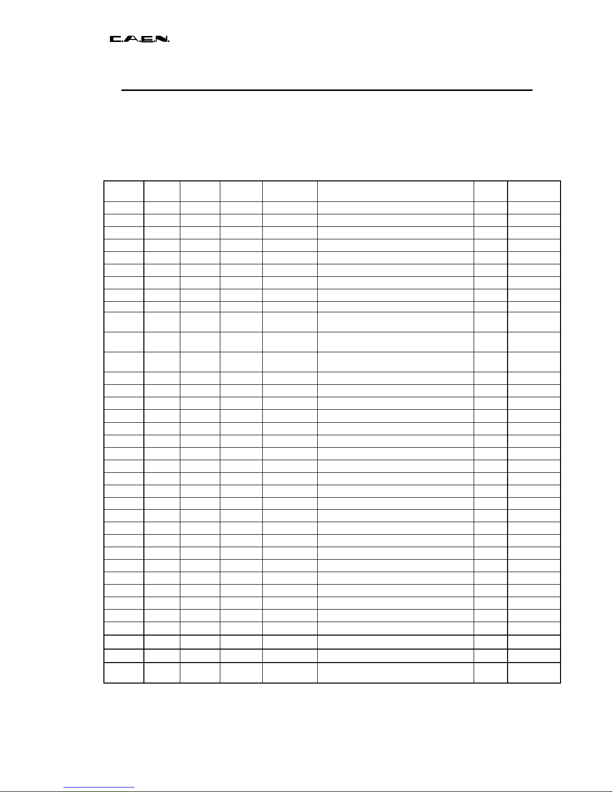
4.8 List of the sub-addresses
The table of the sub-addresses corresponding to the different commands is presented
below. A certain number among them are reserved for expert usage. They are indicated
by the word « RESERVED » in the « NAME » column. They will not be described in this
document and they should not be used. In VME, the sub-addresses are coded over the
bits A8 to A15, the bits A1 to A7 being unused. For more detail on the addressing in VME
or GPIB.
Subadd
(HEX) GPIB VME ACCESS REG or COM. NAME
bits of
data
Default
@ power_on
08 YES YES
W Com RESET BOARD NO
-
09 YES YES
W Com LOAD TRIGGER THRESHOLD DAC NO
-
12 YES YES
W Com RESERVED NO
-
13 YES YES
W Com RESERVED NO
-
14 YES YES
W Com RESERVED NO
-
15 YES YES
W Com RESERVED NO
-
16 YES YES
W Com RESERVED NO
-
17 YES YES
W Com START ACQUISITION NO
-
1C YES YES
W Com SOFTWARE TRIGGER NO
-
0A YES NO
W/R** Reg
TRIGGER THRESHOLD DAC LSB (byte-
>GPIB) 8
0
0B YES NO
W/R** Reg
TRIGGER THRESHOLD DAC MSB
(half byte->GPIB) 4
0
0A NO YES
W/R Reg
TRIGGER THRESHOLD DAC
(word->VME) 12
0
0C YES NO
R Reg RAM DATA MSB + LSB -> GPIB 8
-
0D NO YES
R Reg RAM DATA ->VME 16
-
0E YES YES
W/R Reg RAM_INT_ADD LSB 8
0
0F YES YES
W/R Reg RAM_INT_ADD MSB 8
0
10 YES YES
W/R Reg MAT CTRL REGISTER LSB 8
0
11 YES YES
W/R Reg MAT CTRL REGISTER MSB 8
0
18 YES YES
W/R Reg PRETRIG LSB 8
0
19 YES YES
W/R Reg PRETRIG MSB 8
40
1A YES YES
W/R Reg POSTTRIG LSB 8
64
1B YES YES
W/R Reg POSTTRIG MSB 8
0
1D YES YES
W/R Reg TRIGGER TYPE 5
0
1E YES YES
W/R Reg TRIGGER CHANNEL SOURCE 4
0
20 YES YES
R Reg TRIG_REC 1
-
21 YES YES
W/R Reg FAST READ MODES 2
0
22 YES YES
W/R Reg NB OF COLS TO READ 7
128
23 YES YES
W/R Reg CHANNEL MASKS 4
h0F
24 YES YES
W/R* Reg RESERVED 8
90
30 YES YES
W/R* Reg
POST STOP LATENCY
8
4
31 YES YES
W/R* Reg
POST LATENCY PRETRIG
8
1
80 YES YES
W/R Reg INTERRUPT 1
0
81 YES YES
W/R Reg FP_FREQUENCY 2
1
82 YES YES
R Reg FPGA VERSION 8
-
83 YES YES
W/R Reg EN_VME_IRQ 1
0
FF YES NO
W Reg
NB OF BYTES TO READ IN BLOCK
MODE (GPIB) 24 (3x8)
1
** : no readback of these registers in GPIB.
Page 32

PRELIMINARY
Document type: Title: Revision date: Revision:
User's Manual (MUT) Mod. V1729 4 Channel 12 Bit Sampling ADC 22/06/2005 3
NPO: Filename: Number of pages: Page:
00109/04:V1729.MUTx/03 V1729_REV3.DOC 38 32
The sub-addresses are organized by type. For more detail on their specific use in VME
or GPIB, refer to 4.6.
The functions of these different commands and registers are described below :
RESET BOARD
: reset of the board. Restores idle state. Does not modify the value
loaded in the different registers.
LOAD TRIGGER THRESHOLD DAC
: permits transfer of the pre-loaded value in the
register of the DAC towards the analog converter itself.
START ACQUISITION
: launches the data acquisition and resets the INTERRUPT
register. When this is finished, the INTERRUPT signal will be validated and transmitted
towards the bus interfaces. This latter signal will also be able to be read at the subaddress h80.
SOFTWARE TRIGGER
: permits generation of a trigger coming from a bus interface.
TRIGGER THRESHOLD DAC
: register of pre-loading of the DAC. This 12-bit register
covers the range from –0.5V (000) to +0.5V (FFF). By GPIB, one has access to the
MSBs and LSBs via 2 distinct sub-addresses. The access is necessarily made in the
order MSB (0B) then LSB (0A). By VME, the access is made via a single sub-address
(0A). After loading of this register, one must transfer the value in the analog converter via
the LOAD_TRIGGER THRESHOLD DAC (09) command.
RAM DATA
: this is the memory where the data is stored. As above, the access to the
data is made differently in GPIB and in VME (see NB OF BYTES TO READ IN BLOCK
MODE). The addressing is indirect, the internal address of the RAM being defined by the
RAM_INT_ADD counter located in the ALTERA.
RAM_INT_ADD
: this 16-bit counter fixes the internal address of the RAM for the bus
access in progress. It is set back to zero by the RESET_BOARD command and by the
interruption at the end of the acquisition phase. For a direct access to an address or a
given group of addresses, one must pre-load it.
MAT CTRL REGISTER
: this is a control register for the acquisition parameters. It covers
9 bits. The bits followed by an asterisk are reserved and must be left at zero.
Bits Name Default Function
0
BWL 0 Regulates the bandwidth of the input amplifiers with BWL1 (see 4.5.4 )
1
BWL1 0 Regulates the bandwidth of the input amplifiers with BWL (see 4.5.4 )
2
EBP 0 At 1, authorizes the bypass of the input signal towards the ADC
3
ELD* - Reserved
4
ENVDLL* 0 Reserved
5
EIR* 0 Reserved
6
EPR 0 At 1, forces the permanent supply of the reading amplifiers
7
EPW 0 At 1, forces the permanent supply of the writing amplifiers
8
ESO 0 At 1, authorizes the SYNC_OUT signal to be output from the board (thanks to
the corresponding strap S4)
PRETRIG : this 16-bit register fixes the delay in periods of Fp between the START
ACQUISITION and the internal authorization to validate a trigger, whatever the source of
the latter. For proper functioning, it must be fixed at a minimum of 5000 for an Fp
frequency of 50MHz and at 10000 for a frequency of 100MHz. By default, its value is
10240.
POSTTRIG
: this 16-bit register fixes the delay in periods of Fp between the trigger and
the stopping of the acquisition. It permits in practice choosing the useful position of the
signal in the window of 2560 cells. By default, its value is 64.
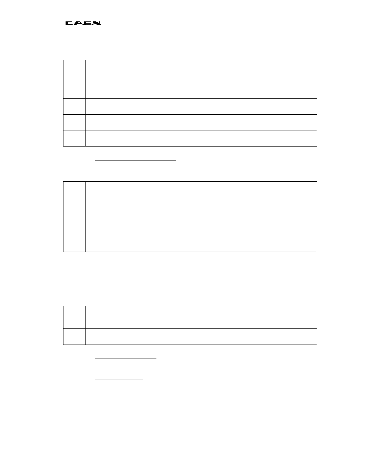
TRIGGER TYPE
: this 5-bit register fixes the source and the useful edge of the trigger.
Page 33
PRELIMINARY
Document type: Title: Revision date: Revision:
User's Manual (MUT) Mod. V1729 4 Channel 12 Bit Sampling ADC 22/06/2005 3
NPO: Filename: Number of pages: Page:
00109/04:V1729.MUTx/03 V1729_REV3.DOC 38 33
Bits Function
0-1
Val = 0 => SOFTWARE TRIGGER
Val = 1 => trigger on discriminator (threshold fixed by the DAC)
Val = 2 => external trigger from the TRIG_EXT input
Val = 3 => logic “OR” of SOFTWARE TRIGGER and trigger on discriminator
2
Val = 0 => rising edge
Val = 1 => falling edge
3
Val = 0 => Inhibites random internal trigger.
Val = 1 => Authorizes random internal trigger.
4
Val = 0 => one uses the Trigger normally.
Val = 1 => one uses the external Trigger directly and without masking.
TRIGGER CHANNEL SOURCE : this 4-bit register fixes the channel(s) from which the
discriminators will release the trigger. More than one channel can be validated at the
same time because one realizes a logic « OR » of the outputs of the discriminators in the
controller.
Bits Function
0
Val = 0 => Disables Trigger on channel 0.
Val = 1 => Enables Trigger on channel 0.
1
Val = 0 => Disables Trigger on channel 1.
Val = 1 => Enables Trigger on channel 1.
2
Val = 0 => Disables Trigger on channel 2.
Val = 1 => Enables Trigger on channel 2.
3
Val = 0 => Disables Trigger on channel 3.
Val = 1 => Enables Trigger on channel 3.
TRIG_REC
: this 8-bit register gives the distance between the column where one finds
the column pointer at the arrival time of the synchronous trigger and the last column
(128). It permits in practice to roughly date the useful signal to the nearest clock rising
edge. This dating will be refined with greater precision by the utilization of the vernier.
FAST READ MODES
: this 2-bit register permits realization of a faster reading of the
MATACQ chips. Usage reserved for experts for it may have an influence on the noise
level.
Bits Function
0
Val = 0 => sequence with reading of TRIG_REC (normal)
Val = 1 => sequence without reading of TRIG_REC (fast)
1
Val = 0 => sequence departing from the first column (normal)
Val = 1 => sequence departing from the STOP (fast)
NB OF COLS TO READ : this 8-bit register gives the number of columns that one wants
to read in the matrix. The number of columns can be fixed between 0 et 128. The stored
value is by default 128, which corresponds to the whole matrix.
CHANNEL MASKS
: each one of the 4 bits in this register individually validates a channel
on the board. For this, they must be set at 1. At zero, the corresponding channel is
masked and its data will not be recorded in the RAM. Caution : this modifies the format of
the frame stored in the RAM (see IV.3).
POST STOP LATENCY
: this register permits the programming with steps of 2.5μs of the
time during which the board waits for the validation signal in the mode where the latter is
Page 34

PRELIMINARY
Document type: Title: Revision date: Revision:
User's Manual (MUT) Mod. V1729 4 Channel 12 Bit Sampling ADC 22/06/2005 3
NPO: Filename: Number of pages: Page:
00109/04:V1729.MUTx/03 V1729_REV3.DOC 38 34
used to launch the readout of the MATACQ chips towards the RAM. The default value is
of 10μs whereas the minimum one is of 2,5μs.
POST LATENCY PRETRIG
: this register fixes with steps of 2.5μs the time given to the
MATACQ chips to get filled up again consequently to the restarting of the writing in the
mode using a validation signal. The default value as well as the minimum one are of
2,5μs.
INTERRUPT
: this register memorizes the arrival of the interruption which signals the end
of the acquisition phase. The INTERRUPT signal is forwarded towards the acquisition
buses, but it can also be read here. It is also here that it must be released and reset at
zero by a simple write access. It is anyhow reset by the START_ACQ command.
FP_FREQUENCY
: this 2-bit register permits fixing of the Fp period. It is initialized at 1.
Bits Function
0-1
Val = 1 => Fsample = 2GHz.
Val = 2 => Fsample = 1GHz.
FPGA VERSION :
this 8-bit read-only register permits reading of the version number of
the FPGA. The 3 MSbits give the type of board and the 5 LSbits the version number of
the firmware stored in the PROM. The code corresponding to the V1729 board is 3,
which gives a root number of h60 for FPGA VERSION.
EN_VME_IRQ :
this 1-bit register permits authorization (1) or not (0) of the output of the
interruption at the end of the acquisition towards the VME bus on VME_IRQ3.
NB OF BYTES TO READ IN BLOCK MODE
: for the readings in block mode by GPIB
solely, this 16-bit register permits fixing the number of bytes contained in the block. In
order to simplify the accesses by reading to the RAM, one will send as in the reading
order 4 bytes of data : the 1
st
with hFF, the 2nd and the 3rd with respectively the LSBs
then the MSBs of the number of bytes to read, and finally the 4
th
with the sub-address
h0C for the RAM. The MSBs then the LSBs will then be sent successively. Do not forget
to double the number of data to read in the RAM when passing from the number of words
to the number of bytes.
Page 35
PRELIMINARY
Document type: Title: Revision date: Revision:
User's Manual (MUT) Mod. V1729 4 Channel 12 Bit Sampling ADC 22/06/2005 3
NPO: Filename: Number of pages: Page:
00109/04:V1729.MUTx/03 V1729_REV3.DOC 38 35
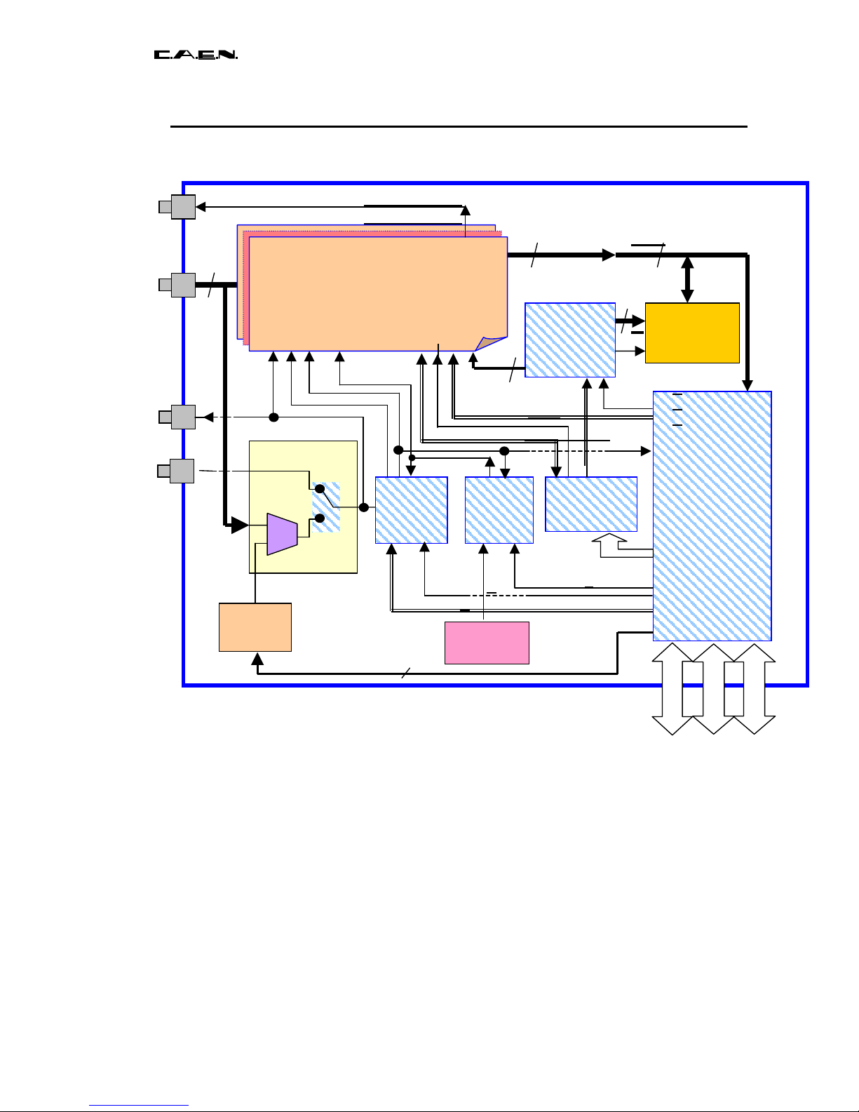
4.9 Synopsis of the board
Fig. 4.3: synopsis of the V1729 board
The architecture of the V1729 board (Fig 4.3) is modulary. This architecture as well as
the components used were selected so as to minimize the costs of conception and
production of the board. The board is principally made up of six blocks :
The 4 channels of acquisition and fast digitization (synopsis of a channel in Fig 4.4).
The management of the trigger.
The management of the clocks.
The slower readout of the MATACQ chips.
The management of writing and of re-reading the digital memory (RAM).
The interfacing with the acquisition system.
The last four blocks (except the RAM itself) as well as the digital part of the trigger
system are integrated in a single programmable component (FPGA). This considerably
reduces the costs of production and will permit an easy upgrading of the system in the
future.
External
trigger
Busy/
Sync_Out
RAM
64k*16bits
1.1.1.2 ADC
RAM
MANAGER
4
Oscillator
100MHz
DAC
thresh
8 canaux
8 canaux
4 channels
1.1.1.3 Output : Busy
or Sync_out
INTERFACE
data
add
R/W
Trigger
Manager
Time
base
Matrix
Controller
Analog
Inputs
Trigger
Trig_Out
1.1.3
.
1.1.3
.
1.1.3
.
1.1.3
.
1.1.3.5 S
1.1.3.6
E
1.1.3.7 P
comp
1.1.3.8 Fast Control
1.1.3.9 Slow
1.1.3.9.1 Output
1
.1.3.9.
2Enable<4
1.1.3.10 CK
1.3.11 RAM Writing
1.1.3.12
RAM
x 4
Page 36
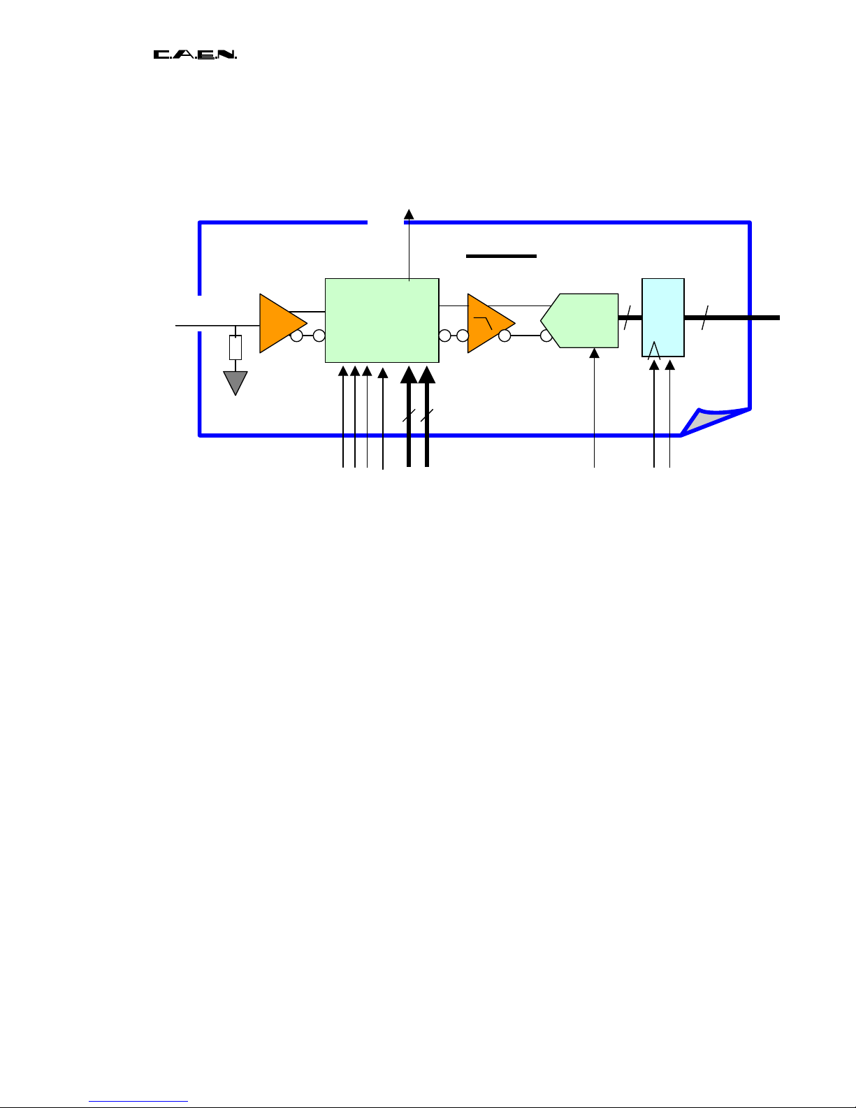
PRELIMINARY
Document type: Title: Revision date: Revision:
User's Manual (MUT) Mod. V1729 4 Channel 12 Bit Sampling ADC 22/06/2005 3
NPO: Filename: Number of pages: Page:
00109/04:V1729.MUTx/03 V1729_REV3.DOC 38 36
The different logical level transfers present on the board are not represented in the
synopsis.
Fig. 4.4: Synopsis of an acquisition channel on the MATACQ board
The elementary block of the analog acquisition is represented in Fig 4.4. It includes:
The 50-Ohm adaptation of the input.
A large bandwidth amplifier making it possible to feed the MATACQ chip in differential.
The MATACQ chip.
A bandwidth limiter filter.
The 12bit-5MHz ADC, differential.
A register allowing the multiplexing of the data coming from the different channels
towards the RAM.
Fast Control
ADCout
BUS
Sample_Reg
MATRIX
2. Filter
ADC
12 12
Analog input
Conversion
: unipolar
->
differential
Register
Clk ADC
Output Enable
Fp
Ta
Ts
Slow Control
Stop
50 Ω
Sync_ Out
Page 37

PRELIMINARY
Document type: Title: Revision date: Revision:
User's Manual (MUT) Mod. V1729 4 Channel 12 Bit Sampling ADC 22/06/2005 3
NPO: Filename: Number of pages: Page:
00109/04:V1729.MUTx/03 V1729_REV3.DOC 38 37
5. Specifications and performances
The following table summarizes the MAIN specifications and performances of the V1729:
Input analog signals
Number of channels 4
Input impedance 50 Ohms
Dynamic Range +/- 0.5V
Bandwidth 300MHz
Noise/signal ratio > 12bit RMS (noise =180 µV RMS)
Harmonic distorsion < -60dB for sinusoidal input at 25MHz
LSB (digitization step) 0.25mV
Integral Non Linearity < 1 per mil
Differential Non Linearity < 0.5 per mil
Relative gain between channels < +-1%
Sampling
Max Frequency 2GS/s
Min Frequency 1GS/s
Time precision in a single channel 15ps RMS typical
Time precision between two channels 20ps RMS typical
Depth per channel 2560 points (of which 2520 are usable)
Trigger
Threshold setting dynamic range +/- 0.5V
Threshold setting step 0.25mV
Time precision 50ps RMS typical (includes both the sampling
and trigger precision)
Analog to Digital Conversion
Conversion frequency 5MHz
Resolution 12 bits
Time to empty the matrices into the RAM 650µs
Acquisition
Acquisitions rate (VME) Up to 500 acquisitions/s over 4 channels
Acquistions rate (GPIB) Up to 100 acquisitions/s over 4 channels
Front Panel Signals (TRIG_OUT, SYNC_OUT, TRIG_EXT)
NIM Standard (negative logics) :
Input Impedance (TRIG_EXT ) 50 Ohms
Lower max level (logic 1) -0.6V
Upper min level (logic 0) -0.2V
Power Supplies
Min voltage on « +5V » 4.5V
Min voltage on « +12V » 6.5V
Min voltage on « -12V » -6.5V
Consumption on +5V 1.5A
Consumption on +12V typ 1A (varies with acquisition rate)
Consumption on -12V typ 1A (varies with acquisition rate)
Page 38

PRELIMINARY
Document type: Title: Revision date: Revision:
User's Manual (MUT) Mod. V1729 4 Channel 12 Bit Sampling ADC 22/06/2005 3
NPO: Filename: Number of pages: Page:
00109/04:V1729.MUTx/03 V1729_REV3.DOC 38 38
6. BIBLIOGRAPHY
[1] E. Delagnes, D. Breton, Echantillonneur analogique rapide à grande profondeur
mémoire.
French patent n°01 05607 from April 26th 2001. US Patent 6,859,375 from February
22nd 2005 : Fast analog sampler with great memory depth.
 Loading...