


CAEN
Tools for Discovery
n
Electronic Instrumentation
User Manual UM3148
DT5730/DT5725
8-Channel 14-bit 500/250 MS/s Digitizer
Rev. 2 - 10 June 2016

Purpose of this Manual
This document contains the full hardware description of the DT5730 and DT5725 digitizers and the principle of operating as
Waveform Digitizer (based on the hereafter called default firmware).
Firmware version of reference: rel. 4.8_0.5
For any reference to registers in this user manual, please refer to document [RD2] at the digitizer web page.
Change Document Record
Date
Revision
Changes
14 February 2014
00
Initial release
15 December 2014
01
Added new § 6 on cooling management and § 7 on temperature protection.
Updated § Trigger Management. General revision.
10 June 2016
02
Fully reviewed to the new DT5725 digitizer (250 MS/s). Updated § 1, § 3, § 5,§ 8, §
Clock Distribution, § PLL Mode, § Trigger Clock, § Channel Calibration, § Custom
Sized Events, § Event Structure, § Trigger Distribution, § DPP-PSD Control
Software, § 13. Added § Changing the ADC Frequency, § CAENScope, §
MC²Analyzer (MC²A)
Symbols, abbreviated terms and notation
GUI
Graphical User Interface
DPP
Digital Pulse Processing
ETTT
Extended Trigger Time Tag
OS
Operating System
PSD
Pulse Shape Discrimination
TTT
Trigger Time Tag
Reference Documents
[RD1] GD2512 – CAENUpgrader QuickStart Guide
[RD2] UM5118 – 725-730 Families Default Firmware Registers
[RD3] GD2783 – First Installation Guide to Desktop Digitizers & MCA
[RD4] UM1934 - CAENComm User & Reference Manual
[RD5] UM1935 - CAENDigitizer User & Reference Manual
[RD6] UM2091 - CAEN WaveDump User Manual
[RD7] GD2483 - WaveDump QuickStart Guide
[RD8] UM2092 - CAENSCOPE User Manual
[RD9] UM2580 - Digital Pulse Shape Discriminator (DPP-PSD) User Manual
[RD10] UM3182 - DPP-PHA and MC
2
Analyzer User Manual
[RD11] GD2728 – How to make Coincidences with CAEN Digitizers
All documents can be downloaded at: http://www.caen.it/csite/LibrarySearch.jsp

CAEN S.p.A.
Via Vetraia, 11 55049 Viareggio (LU) - ITALY
Tel. +39.0584.388.398 Fax +39.0584.388.959
info@caen.it
www.caen.it
© CAEN SpA – 2016
Disclaimer
No part of this manual may be reproduced in any form or by any means, electronic, mechanical, recording, or
otherwise, without the prior written permission of CAEN SpA.
The information contained herein has been carefully checked and is believed to be accurate; however, no responsibility
is assumed for inaccuracies. CAEN SpA reserves the right to modify its products specifications without giving any
notice; for up to date information please visit www.caen.it.
MADE IN ITALY : We stress the fact that all the boards are made in Italy because in this globalized world, where getting
the lowest possible price for products sometimes translates into poor pay and working conditions for the people who
make them, at least you know that who made your board was reasonably paid and worked in a safe environment. (this
obviously applies only to the boards marked "MADE IN ITALY", we cannot attest to the manufacturing process of "third
party" boards).

CAEN
Electronic Instrumentation
UM3148 – DT5730/DT5725 User Manual rev. 2
4
Index
Purpose of this Manual ....................................................................................................................... 2
Change Document Record ................................................................................................................ 2
Symbols, abbreviated terms and notation ....................................................................................... 2
Reference Documents ........................................................................................................................ 2
Index ........................................................................................................................................ 4
List of Figures......................................................................................................................... 5
List of Tables .......................................................................................................................... 5
1 Introduction ..................................................................................................................... 6
2 Block Diagram ................................................................................................................ 8
3 Technical Specifications ............................................................................................... 9
4 Packaging and Compliancy ........................................................................................ 10
5 Power Requirements ................................................................................................... 11
6 Cooling Management ................................................................................................... 12
7 Temperature Protection .............................................................................................. 13
8 Panels Description ....................................................................................................... 14
Front Panel ......................................................................................................................................... 15
Rear Panel .......................................................................................................................................... 18
9 Functional Description ................................................................................................ 19
Analog Input Stage ............................................................................................................................ 19
Clock Distribution ............................................................................................................................... 20
PLL Mode............................................................................................................................................ 21
Changing the ADC Frequency......................................................................................................... 21
Trigger Clock ...................................................................................................................................... 21
Acquisition Modes ............................................................................................................................. 22
Channel Calibration ..................................................................................................................................... 22
Acquisition Run/Stop .................................................................................................................................. 26
Acquisition Triggering: Samples & Events ........................................................................................... 27
Multi-Event Memory Organization ........................................................................................................... 28
Custom Sized Events .....................................................................................................................................................28
Event Structure ............................................................................................................................................. 29
Event Format Example ...................................................................................................................................................30
Acquisition Synchronization ..................................................................................................................... 31
Trigger Management ......................................................................................................................... 32
Software Trigger ........................................................................................................................................... 32
External Trigger ............................................................................................................................................ 32
Self-Trigger .................................................................................................................................................... 33
Trigger Coincidence Level ......................................................................................................................... 35
Trigger Distribution ..................................................................................................................................... 39
Example ...........................................................................................................................................................................40
Reset, Clear and Default Configuration ......................................................................................... 41
Global Reset .................................................................................................................................................. 41
Memory Reset ............................................................................................................................................... 41
Timer Reset .................................................................................................................................................... 41
Data Transfer Capabilities ................................................................................................................ 42
Block Transfers ............................................................................................................................................ 42
Single Data Transfer .................................................................................................................................... 42
Optical Link and USB Access .......................................................................................................... 43
10 Drivers & Libraries ....................................................................................................... 44
Drivers ................................................................................................................................................. 44
Libraries .............................................................................................................................................. 44
11 Software Tools .............................................................................................................. 46

CAEN
Electronic Instrumentation
UM3148 – DT5730/DT5725 User Manual rev. 2
5
CAENUpgrader .................................................................................................................................. 46
CAENComm Demo ........................................................................................................................... 47
CAEN WAVEDump ........................................................................................................................... 48
CAENScope ....................................................................................................................................... 49
DPP-PSD Control Software ............................................................................................................. 50
MC²Analyzer (MC²A) ......................................................................................................................... 51
12 HW Installation.............................................................................................................. 52
Power-on Sequence .......................................................................................................................... 52
Power-on Status ................................................................................................................................ 52
13 Firmware and Upgrades .............................................................................................. 53
Default Firmware Upgrade ............................................................................................................... 54
Upgrade Files Description ......................................................................................................................... 54
DPP Firmware Upgrade .............................................................................................................................. 54
Upgrade File Description ...............................................................................................................................................54
14 Technical Support ........................................................................................................ 55
Returns and Repairs ......................................................................................................................... 55
Technical Support Service ............................................................................................................... 55
List of Figures
Fig. 2.1: Block Diagram ........................................................................................................................................................................8
Fig. 4.1: Front view .............................................................................................................................................................................10
Fig. 5.1: AC/DC power supply provided with the module ..............................................................................................................11
Fig. 8.1: Front panel view ..................................................................................................................................................................14
Fig. 8.2: Rear panel view ...................................................................................................................................................................14
Fig. 9.1: Analog Input Diagram .........................................................................................................................................................19
Fig. 9.2: Clock Distribution Diagram .................................................................................................................................................20
Fig. 9.3: Typical channel before the calibration (A and B) and after the calibration (C) ...........................................................22
Fig. 9.4: Automatic calibration at WaveDump first run ..................................................................................................................24
Fig. 9.5: Temperature monitoring with manual calibration in WaveDump software ..................................................................24
Fig. 9.6: Channel calibration in DPP-PSD Control Software ........................................................................................................25
Fig. 9.7: Channel calibration in MC2Analyzer software .................................................................................................................25
Fig. 9.8: Trigger overlap .....................................................................................................................................................................27
Fig. 9.9: Block Diagram of the trigger management ......................................................................................................................32
Fig. 9.10: Self Trigger and Trigger Request logic for Ch0 and Ch1 couple. A single trigger request signal is generated...33
Fig. 9.11: Channel over/under threshold signal ..............................................................................................................................33
Fig. 9.12: Channel pulse signal ........................................................................................................................................................34
Fig. 9.13: Trigger request management at mezzanine level with Majority level = 0 .................................................................36
Fig. 9.14: Trigger request management at motherboard level with Majority level = 0 ..............................................................36
Fig. 9.15: Trigger request relationship with Majority level = 1 and T
TVAW
≠ 0 .............................................................................37
Fig. 9.16: Trigger request relationship with Majority level = 1 and T
TVAW
= 0 .............................................................................38
Fig. 9.17: Trigger configuration on GPO front panel output connector .......................................................................................39
Fig. 10.1: Required libraries and drivers ..........................................................................................................................................45
Fig. 11.1: CAENUpgrader Graphical User Interface ......................................................................................................................46
Fig. 11.2: CAENComm Demo Java and LabVIEW graphical interface .......................................................................................47
Fig. 11.3: CAEN WaveDump ............................................................................................................................................................48
Fig. 11.4: CAENScope main frame ..................................................................................................................................................49
Fig. 11.5: DPP-PSD Control Software: Top – DPP settings Tab and typical 60Co Total Charge Spectrum; Bottom - PSD
2-D Scatter Plot ...................................................................................................................................................................................50
Fig. 11.6: MC²Analyzer (MC²A) software tool .................................................................................................................................51
Fig. 12.1: Front panel LEDs status at power ON............................................................................................................................52
List of Tables
Tab. 1.1: Table of models and related items .....................................................................................................................................7
Tab. 3.1: Specifications table ..............................................................................................................................................................9
Tab. 9.1: Buffer Organization ............................................................................................................................................................28
Tab. 9.2: TRG OPTIONS configuration table .................................................................................................................................29
Tab. 9.3: Event Format Example ......................................................................................................................................................30

CAEN
Electronic Instrumentation
UM3148 – DT5730/DT5725 User Manual rev. 2
6
1 Introduction
The DT5730 is a Desktop module housing a 8-channel 14-bit 500 MS/s FLASH ADC Waveform Digitizer with software
selectable 2 Vpp or 0.5 Vpp input dynamic range on single ended MCX coaxial connectors. The DC offset is adjustable in
the ±1 V (@ 2 Vpp) or ±0.25 (@ 0.5 Vpp) range via a 16-bit DAC on each channel (see § Analog Input Stage).
Operationally, the mod. DT5725 differs from the DT5730 for working at 250 MS/s sampling frequency.
The ADC resolution and the sampling frequency make these digitizers well suited for mid-fast signal detection systems
(e.g. liquid or inorganic scintillators coupled to PMTs or Silicon Photomultipliers).
Each channel has a SRAM Multi-Event Buffer divisible into 1 ÷ 1024 buffers of programmable size. Two sizes of the
channel digital memory are available by ordering option (see Tab. 1.1).
DT5730 and DT5725 digitizers are provided with FPGAs that can run special DPP firmware for Physics Applications (see
§ 13).
A common acquisition trigger signal can be fed externally via the front panel TRG-IN input connector or via software.
Alternatively, each channel is able to generate a self-trigger when the input signal goes under/over a programmable
threshold. For each couple of adjacent channels, the relevant self-triggers are then processed to provide out a single
trigger request. In the DPP firmware, the trigger requests can be used at channel level for the event acquisition
(independent triggering), while in the default firmware they can be processed by the board to generate a common
trigger causing all the channels to acquire an event simultaneously. The trigger from one board can be propagated to
the other boards through the front panel GPO output connector.
During the acquisition, the data stream is continuously written in a circular memory buffer. When the trigger occurs,
the digitizer writes further samples for the post trigger and freezes the buffer that can be read by one of the provided
readout links. The acquisition can continue without any dead time in a new buffer.
DT5730 and DT5725 feature front panel CLK-IN connector as well as an internal PLL for clock synthesis from
internal/external references. Multi-board synchronization is supported, so all DT5730 or all DT5725 can be
synchronized to a common clock source and ensuring Trigger time stamps alignment. The fan-in of an external clock
signal to each CLK-IN is required. Once synchronized, all data will be aligned and coherent across the multi-board
system.
Each module houses USB 2.0 and Optical Link interfaces. USB 2.0 allows data transfers up to 30 MB/s. The Optical Link
(CAEN proprietary CONET protocol) supports transfer rate of 80 MB/s and offers Daisy chain capability. Therefore, it is
possible to connect up to 8 ADC modules to a single A2818 Optical Link Controller, or up to 32 using a A3818 (4-link
version). Optical Link and USB accesses are internally arbitrated.

CAEN
Electronic Instrumentation
UM3148 – DT5730/DT5725 User Manual rev. 2
7
Board Models
Description
Product Code
DT5730
DT5730 - 8 ch. 14bit 500 MS/s Digitizer: 640kS/ch,CE30, SE
WDT5730XAAAAA
DT5730B
DT5730B - 8 ch. 14bit 500 MS/s Digitizer: 5.12MS/ch,CE30, SE
WDT5730BXAAAA
DT5725
DT5725 - 8 ch. 14bit 250 MS/s Digitizer: 640kS/ch,CE30, SE
WDT5725XAAAAA
DT5725B
DT5730B - 8 ch. 14bit 250 MS/s Digitizer: 5.12MS /ch,CE30, SE
WDT5725BXAAAA
DPP Firmware⁽*⁾
Description
Product Code
DPP-PSD
(730 family)
DPP-PSD - Digital Pulse Processing for Pulse Shape Discrimination (x730)
WFWDPPNGAA30
DPP-PSD
(725 family)
DPP-PSD - Digital Pulse Processing for Pulse Shape Discrimination (x725)
WFWDPPNGAA25
DPP-PHA
(730 family)
DPP-PHA - Digital Pulse Processing for Pulse Height Analysis (x730)
WFWDPPTFAA30
DPP-PHA
(725 family)
DPP-PHA - Digital Pulse Processing for Pulse Height Analysis(x725)
WFWDPPTFAA25
Related Products
Description
Product Code
A2818
A2818 – PCI Optical Link (Rhos compliant)
WA2818XAAAAA
A3818A
A3818A – PCIe 1 Optical Link
WA3818AXAAAA
A3818B
A3818B – PCIe 2 Optical Link
WA3818BXAAAA
A3818C
A3818C – PCIe 4 Optical Link
WA3818CXAAAA
Accessories
Description
Product Code
A317
Clock Distribution Cable
WA317XAAAAAA
A318
SE to Differential Clock Adapter
WA318XAAAAAA
A654
Single Channel MCX to LEMO Cable Adapter
WA654XAAAAAA
A654 KIT4
4 MCX TO LEMO Cable Adapter
WA654K4AAAAA
A654 KIT8
8 MCX TO LEMO Cable Adapter
WA654K8AAAAA
A659
A659 - Single Channel MCX to BNC Cable Adapter
WA659XAAAAAA
A659 KIT4
4 MCX TO BNC Cable Adapter
WA659K4AAAAA
A659 KIT8
8 MCX TO BNC Cable Adapter
WA659K8AAAAA
AI2730
Optical Fibre 30 m simplex
WAI2730XAAAA
AI2720
Optical Fibre 20 m simplex
WAI2720XAAAA
AI2705
Optical Fibre 5 m simplex
WAI2705XAAAA
AI2703
Optical Fibre 30 cm simplex
WAI2703XAAAA
AY2730
Optical Fibre 30 m duplex
WAY2730XAAAA
AY2720
Optical Fibre 20 m duplex
WAY2720XAAAA
AY2705
Optical Fibre 5 m duplex
WAY2705XAAAA
Tab. 1.1: Table of models and related items
⁽*⁾ Multi-license packs are also available. Please, refer to the Digitizer web page for the relevant ordering options.

CAEN
Electronic Instrumentation
UM3148 – DT5730/DT5725 User Manual rev. 2
8
2 Block Diagram
DAC
AMC [FPGA]
ADC &
MEMORY
CONTROLLER
ADC
BUFFERS
x8 channels
ROC [FPGA]
- Readout Controller
- Optical link Interface
- USB interface
- Global Trigger Logic
- I/O Control Logic
MUX
OSC
CLOCK
MANAGER
(AD9520)
LOCAL BUS
CLK IN
TRG IN
GPI
USB
INPUTS
FRONT PANEL
GPO
OPTICAL LINK
G1 or G4
PGA
Fig. 2.1: Block Diagram

CAEN
Electronic Instrumentation
UM3148 – DT5730/DT5725 User Manual rev. 2
9
3 Technical Specifications
GENERAL
Form Factor 154x50x164 mm3 (WxHxD) Desktop
ANALOG INPUT
Channels
8 channels
Single ended
Connector
MCX
Bandwidth
250 MHz (DT5730)
125 MHz (DT5725)
Impedance
Zin = 50 Ω
Full Scale Range
0.5 or 2 Vpp (default)
SW selectable
Offset
Programmable 16-bit
DAC for DC offset
adjustment on each
channel.
Range: ±1 V (@2Vpp);
±0.25 V (@0.5Vpp)
DIGITAL CONVERSION
Resolution
14 bits
Sampling Rate
500 MS/s Simultaneously on each channel (DT5730
250 MS/s Simultaneously on each channel (DT5725)
ADC CLOCK GENERATION
Clock source: internal/external
On-board programmable PLL provides generation of the main board clocks from an internal (50 MHz
local Oscillator) or external (front panel CLK-IN connector) reference
DIGITAL I/O
CLK-IN (AMP Modu II)
AC coupled differential input clock.
LVDS, ECL, PECL, LVPECL, CML
(single ended NIM/TTL available by CAEN
adapter)
Jitter<100ppm requested
TRG-IN (LEMO)
External trigger digital input
NIM/TTL, Z
in
= 50 Ω
GPO (LEMO)
General purpose digital output
NIM/TTL, Rt = 50 Ω
GPI (LEMO)
General purpose digital input
NIM/TTL, Zin = 50 Ω
MEMORY
640 kS/ch or 5.12 MS/s Multi-event Buffer divisible into 1 ÷ 1024 buffers
Independent read and write access; programmable event size and pre/post-trigger
TRIGGER
Trigger Source
Self-trigger: channel over/under-
threshold for Common or Individual (DPP
firmware only) Trigger generation
External-trigger: Common trigger by
TRG-IN connector
Software-trigger: Common trigger by
software command
Trigger Propagation
GPO programmable digital output
Trigger Time Stamp
Default FW: 31-bit counter, 16 ns resolution, 17 s range;
48-bit extension available by firmware
DPP-PHA/DPP-PSD FW (DT5730): 31-bit counter, 2 ns
resolution, 4 s range; 47-bit extension available by
firmware; 10-bit and 2 ps fine time stamp by digital CFD
(DPP-PSD FW only); 64-bit extension available by software
DPP-PHA/DPP-PSD FW (DT5725): 31-bit counter, 4 ns
resolution, 8 s range; 47-bit extension available by
firmware; 10-bit and 4 ps fine time stamp by digital CFD
(DPP-PSD FW only); 64-bit extension available by software
SYNCHRONIZATION
Clock Propagation
One-to-many: clock distribution from an
external clock source on CLK-IN
connector
Acquisition Synchronization
Sync, Start/Stop through digital I/O (TRG-IN or GPI input,
GPO output)
Trigger Time Stamps Alignment
By GPI input connector
ADC & MEM. CONTROLLER
Altera Cyclone EP4CE30 (one FPGA serves 4 channels)
COMMUNICATION
INTERFACE
Optical Link
CAEN CONET proprietary protocol
Up to 80 MB/s transfer rate
Daisy chainable: it is possible to
connect up to 8 or 32 ADC modules to a
single Optical Link Controller
(respectively A2818 or A3818)
USB
USB 2.0 compliant
Up to 30 MB/s transfer rate
DPP FW SUPPORTED
DPP-PSD for the Pulse Shape Discrimination (e.g. Neutron-Gamma discrimination)
DPP-PHA for the Pulse Height Analysis
FIRMWARE UPGRADE
Firmware can be upgraded via USB/Optical Link
SOFTWARE
General purpose C libraries, configuration tools, readout software (Windows and Linux support)
POWER CONSUMPTIONS
DT5730
2.8 A @ 12 V (Typ.)
DT5725
t.b.d. Tab. 3.1: Specifications table

CAEN
Electronic Instrumentation
UM3148 – DT5730/DT5725 User Manual rev. 2
10
4 Packaging and Compliancy
DT5725 and DT5730 modules are Desktop boards housed in a 154 W x 50 H x 164 D mm³ alloy box.
Fig. 4.1: Front view
CAUTION: to manage the product, consult the operating instructions provided.
A POTENTIAL RISK EXISTS IF THE OPERATING INSTRUCTIONS ARE NOT
FOLLOWED!
CAEN provides the specific document “Precautions for Handling, Storage and
Installation” available in the documentation tab of the product web page that the user
is mandatory to read before to operate with CAEN equipment.

CAEN
Electronic Instrumentation
UM3148 – DT5730/DT5725 User Manual rev. 2
11
5 Power Requirements
Both DT5725 and DT5730 modules are powered by the external AC/DC stabilized power supply provided with the
digitizer and included in the delivered kit.
The DT5730 typical power consumption is 2.8 A (@ +12 V).
Note.: Using a different power supply source, like battery or linear type, it is recommended the source to provide +12
V and, at least, 3.5 A in case of DT5730; the power jack is a 2.1 mm type, a suitable cable is the RS 656-3816 type (or
similar)
Fig. 5.1: AC/DC power supply provided with the module

CAEN
Electronic Instrumentation
UM3148 – DT5730/DT5725 User Manual rev. 2
12
6 Cooling Management
Starting from revision 4 of the motherboard (readable at 0xF04C address of the Configuration ROM), DT5730 and
DT5725 feature an automatic fan speed control to guarantee an appropriate cooling in consequence of internal
temperature variations. The automatic control is managed by the ROC FPGA firmware from revision 4.4 on.
CAEN HEARTLY RECOMMENDS TO MONITOR THE TEMPERATURE OF THE ADC CHIPS DURING THE BOARD
OPERATION BY READING AT REGISTER ADDRESS 0x1nA8.
The user can manually set the fan speed through the bit[3] at register address 0x8168 (refer to [RD2]):
Hardware revision ≥ 4 and ROC FPGA firmware revision ≥ 4.4
• Bit[3] = 0 (default) sets the automatic fan speed control;
• Bit[3] = 1 sets HIGH the fan speed.
Hardware revision < 4 and ROC FPGA firmware revision < 4.4
• Bit[3] = 0 (default) sets LOW the fan speed;
• Bit[3] = 1 sets HIGH the fan speed.
WARNING: It is recommended not to run ROC FPGA firmware revision < 4.4 on DT5730 or DT5725 with hardware
revision ≥ 4 as the fans will work always at the maximum speed to prevent from hardware damages, but with a high
noisiness on the other hand.

CAEN
Electronic Instrumentation
UM3148 – DT5730/DT5725 User Manual rev. 2
13
7 Temperature Protection
TEMPERATURE PROTECTION IS NOT AVAILABLE FOR DEFAULT FIRMWARE RELEASES < 4.5_0.3 (REFER TO § 13)
To preserve hardware damages, DT5730 and DT5725 implement an automatic turning off of the board channels in
event of internal over-temperature. Internal temperature can be monitored through register address 0x1nA8.
The over-temperature limit is fixed at 70°C. As soon as the internal temperature exceeds 70°C, the board enters the
temperature protection condition and the firmware automatically performs the following actions:
• turns off all the channel ADCs;
• stops the acquisition, if running (data possibly stored at that moment can be readout in any case).
This status is valid as long as the internal temperature remains over 62°C. Starting from 61°C, the user is allowed to
turn on the channel ADCs again and restart the acquisition, if necessary.
The temperature protection can be controlled through register addresses 0x8104 and 0x81C0.

CAEN
Electronic Instrumentation
UM3148 – DT5730/DT5725 User Manual rev. 2
14
8 Panels Description
Fig. 8.1: Front panel view
Fig. 8.2: Rear panel view

CAEN
Electronic Instrumentation
UM3148 – DT5730/DT5725 User Manual rev. 2
15
Front Panel
ANALOG INPUT
FUNCTION
Input connectors (CH0 to CH7) receiving the
input analog signals.
ELECTRICAL SPECS
Input dynamics: 2 or 0.5 Vpp (SW selectable)
Input impedance (Zin): 50 Ω.
MECHANICAL SPECS
Series: MCX connectors.
Type: CS 85MCX-50-0-16.
Manufacturer: SUHNER
Suggested plug: MCX-50-2-16 type.
Suggested cable: RG174 type.
CLK IN
FUNCTION
Input connector for the external clock.
ELECTRICAL SPECS
Sign. type: differential (LVDS, ECL, PECL, LVPECL,
CML). CAEN provides single-ended to differential
A318 cable adapter (see Tab. 1.1) for CLK-IN.
Coupling: AC.
Z
diff
: 100 Ω.
MECHANICAL SPECS
Series: AMPMODU connectors.
Type: 3-102203-4 (3-pin).
Manufacturer: AMP Inc.
PINOUT
CLK IN LED (GREEN): indicates the external clock is enabled.

CAEN
Electronic Instrumentation
UM3148 – DT5730/DT5725 User Manual rev. 2
16
GPO
FUNCTION
General purpose programmable digital output
connector to propagate:
the internal trigger sources;
the channel probes (i.e. signals from the
mezzanines);
GPI signal
according to register addresses 0x8110 and
0x811C, or
the motherboard probes (i.e. signals
from the motherboard), like the Run
signal, ClkOut signal, ClockPhase signal,
PLL_Unlock signal or Busy signal
according to register address 0x811C.
ELECTRICAL SPECS
Signal level: NIM or TTL.
Requires 50 Ω termination.
MECHANICAL SPECS
Series: 101 A 004 connectors.
Type: DLP 101 A 004-28.
Manufacturer: FISCHER.
Alternatively:
Type: EPL 00 250 NTN.
Manufacturer: LEMO.
TRG IN
FUNCTION
Digital input connector for the external trigger.
ELECTRICAL SPECS
Signal level: NIM or TTL.
Input impedance (Zin): 50 Ω.
MECHANICAL SPECS
Series: 101 A 004 connectors.
Type: DLP 101 A 004-28.
Manufacturer: FISCHER.
Alternatively:
Type: EPL 00 250 NTN.
Manufacturer: LEMO.
GPI
FUNCTION
General purpose programmable input connector.
Can be used to reset the time stamp (see § Timer
Reset) or to start/stop the acquisition.
ELECTRICAL SPECS
Signal level: NIM or TTL.
Input impedance (Zin): 50 Ω.
MECHANICAL SPECS
Series: 101 A 004 connectors.
Type: DLP 101 A 004-28.
Manufacturer: FISCHER.
Alternatively:
Type: EPL 00 250 NTN.
Manufacturer: LEMO.

CAEN
Electronic Instrumentation
UM3148 – DT5730/DT5725 User Manual rev. 2
17
OPTICAL LINK PORT
FUNCTION
Optical LINK connector for data readout and flow
control. Daisy chainable. Compliant to Multimode
62.5/125μm cable featuring LC connectors on both
sides.
ELECTRICAL SPECS
Transfer rate: up to 80 MB/s.
MECHANICAL SPECS
Series: SFF Transceivers.
Type: FTLF8519F-2KNL (LC connectors).
Manufacturer: FINISAR.
PINOUT
LINK LEDs (GREEN/YELLOW): right LED (GREEN) indicates the network presence, while left LED (YELLOW) signals the
data transfer activity.
USB PORT
FUNCTION
USB connector for data readout and flow control.
ELECTRICAL SPECS
Standard: compliant to USB 2.0 and USB 1.0.
Transfer rate: up to 30 MB/s.
MECHANICAL SPECS
Series: USB connectors.
Type: 787780-2 (B-Type).
Manufacturer: AMP Inc.
USB LINK LED (GREEN): indicates the USB communication is active.
DIAGNOSTICS LEDs
TTL (GREEN): indicates the TTL standard is set for GPO, TRG IN, GPI;
NIM (GREEN): indicates the NIM standard is set for GPO, TRG IN, GPI;
PLL LOCK (GREEN): indicates the PLL is locked to the reference clock;
PLL BYPS (GREEN): indicates the PLL drives directly the ADCs. PLL circuit is
switched off and PLL LOCK LED is turned off;
RUN (GREEN): indicates the acquisition is running (data taking). See § Acquisition
Run/Stop;
TRG (GREEN): indicates the trigger is accepted.
DRDY (GREEN): indicates the event/data is present in the Output Buffer.
BUSY (RED): indicates all the buffers are full for at least one channel.

CAEN
Electronic Instrumentation
UM3148 – DT5730/DT5725 User Manual rev. 2
18
Rear Panel
SPARE LINK
FUNCTION
Auxiliary connector reserved for CAEN usage.
ELECTRICAL SPECS
Not available.
MECHANICAL SPECS
Series: Header connectors.
Type: 7610-5002-5+5.
Manufacturer: 3M.
DC INPUT
FUNCTION
Input connector for the desktop Digitizer main
power supply from the external AC/DC adapter.
ELECTRICAL SPECS
Typ. Input voltage: +12 VDC.
MECHANICAL SPECS
Series: CC power supply connectors
Type: RAPC722X (DC power jack).
Manufacturer: Switchcraft Inc.
PINOUT
C
ON/OFF SWITCH
FUNCTION
Panel switch for module power supply
ON/OFF:
O → power supply OFF.
I → power supply ON.
ELECTRICAL SPECS
Not available.
MECHANICAL SPECS
Series: A1 switches.
Type: A11331122000 (Single pole two way)
Manufacturer: Molveno.
IDENTIFYING LABEL
FUNCTION
Board’s identifying label indicating:
the model;
the serial number (S/N);
the symbol of the CE conformity marking.

CAEN
Electronic Instrumentation
UM3148 – DT5730/DT5725 User Manual rev. 2
19
9 Functional Description
Analog Input Stage
Input dynamics can be 2 V
pp
(default) or 0.5 V
pp
, by software selection (basing on the Programmable Gain Amplifier in
the scheme of Fig. 9.1), on single ended MCX coaxial connectors (see § 8). A 16-bit DAC allows to add a DC offset in
order to preserve the full dynamic range also in the extreme case of unipolar positive or negative input signal. The
input bandwidth ranges from DC to 250 MHz (@3dB) for DT5730, to 125 MHz (@3dB) for DT5725, by 2nd order linear
phase anti-aliasing low-pass filter.
+1.00
0
+2.00
-1.00
-2.00
Input Dynamic Range: 2 Vpp
Positive Unipolar
DAC = FSR
Negative Unipolar
DAC = 0
Bipolar
DAC = FSR/2
+0.25
0
-0.50
-0.25
-0.50
Input Dynamic Range: 0.5 Vpp
Positive Unipolar
DAC = FSR
Negative Unipolar
DAC = 0
Bipolar
DAC = FSR/2
MCX
OpAmp
50ohm
DAC
Vref
14 bit
ADC
Input
FPGA
16 bit
+
-
DC Offset
PGA
G1 or G4
Fig. 9.1: Analog Input Diagram
Setting the input range requires a write access at register address 0x1n28, while at register address 0x1n98 it is
possible to configure the DC offset level.

CAEN
Electronic Instrumentation
UM3148 – DT5730/DT5725 User Manual rev. 2
20
Clock Distribution
The module clock distribution takes place on two domains: OSC-CLK and REF-CLK; the former is a fixed 50MHz clock
provided by an on- board oscillator, the latter provides the ADC sampling clock.
OSC-CLK handles Local Bus (communication between motherboard and mezzanine boards; see red traces in Fig. 9.2).
REF-CLK handles ADC sampling, trigger logic, acquisition logic (samples storage into RAM, buffer freezing on trigger)
through a clock chain. Such domain can use either an external (via front panel signal on CLK-IN) or an internal (via local
oscillator) source; in the latter case, OSC-CLK and REF-CLK will be synchronous (the operation mode remains the same
anyway).
DT5730 and DT5725 use an integrated phase-locked-loop (PLL) and clock distribution device, AD9520. It is used to
generate the sampling clock for ADCs and the mezzanine FPGA (SAMP-CLK0/SAMP-CLK1), as well as the trigger logic
synchronization clock (TRG-CLK).
Both clocks can be generated from the internal oscillator (50 MHz) or from external clock input. By default, the board
uses the internal clock as PLL reference (REF-CLK).
The external clock can be selected by write access at register address 0x8100 (refer to [RD2]). The external clock signal
must be differential (LVDS, ECL, PECL, LVPECL, CML) with a jitter lower than 100ppm (see § Tab. 3.1).
AD9520 configuration can be changed and stored into non-volatile memory. Changing the AD9520 configuration is
primarily intended to be used for external PLL reference clock frequency change:
DT5730 and DT5725 lock to an external 50 MHz clock with default AD9520 configuration (see § PLL Mode).
Refer to the AD9520 datasheet for more details:
http://www.analog.com/static/imported-files/data_sheets/AD9520-3.pdf
(in case the active link above doesn’t work, copy and paste it on the internet browser)
MUX
OSC
CLK IN
50MHz
REF-CLK
Trigger & Sync
Logic
TRG IN
LOCAL BUS
Local Bus
Interface
Acquisition
& Memory
Control
Logic
MEZZANINE
TRIGGER
SYNC
LOCAL-TRGs
MUX
Phase
Detector
AD9520
CLK1
Sdiv
Sdiv
Rdiv
REFIN
INTCLK
CTRL
Ldiv
Odiv
Ndiv
SAMP-CLK0
FPGA (AMC)
ADC
CH7
SCLK
DATA
SYNC
SRAM
FIFO
ADC
CH0
SCLK
DATA
Ldel
Odel
Local Bus
Interface
FPGA (ROC)
SYNCB
TRG-CLK
SyncB
RAMCLK
DATA
FANOUT
OSC-CLK
SAMP-CLK1
4
DFF
VCXO
.
.
.
.
.
.
.
.
Fig. 9.2: Clock Distribution Diagram

CAEN
Electronic Instrumentation
UM3148 – DT5730/DT5725 User Manual rev. 2
21
PLL Mode
The Phase Detector within the AD9520 device allows to couple REF-CLK with a VCXO (500 MHz frequency) providing
out the nominal ADCs frequency (500 MHz for DT5730 and 250 MHz for DT5725); for this purpose, it is necessary that
REF-CLK is a submultiple of the VCXO frequency.
As introduced in § Clock Distribution, the source of the REF-CLK signal can be external (see Fig. 9.2) on CLK-IN front
panel connector or internal from the 50 MHz local oscillator. The following options are allowed:
1. 50 MHz internal clock source – It’s the standard operating mode, where the default AD9520 configuration
doesn’t require to be changed. OSC-CLK = REF-CLK.
2. 50 MHz external clock source – In this case it is not required to reprogram the AD9520 dividers, as the external
clock reference is identical to the frequency of the internal oscillator. CLK-IN = OSC-CLK = REF-CLK.
Note that, In order the board to sense the external signal on CLK-IN and use it as new reference, bit[6] at
register address 0x8100 must be set (see [RD2]).
3. External clock source different from 50 MHz – In this case, the user is required to program the AD9520 dividers
in order to lock the VCXO to REF-CLK in order to provide out the 500 MHz (DT5730) or 250 MHz (DT5725)
nominal sampling frequency. In principle, the allowed external frequencies are submultiples of the VCXO
frequency (500 MHz). CLK-IN = REF-CLK.
Note: the user who wants to work as in point 3, please contact CAEN indicating the required reference clock frequency
to check its feasibility and then receive the PLL programming file. The “Upgrade PLL” function in CAENUpgrader
software tool can be used to update the digitizer PLL. See § 11 for the program description and refer to [RD1] for
documentation. The programming file also takes care to set the board to sense the external signal on CLK-IN.
Changing the ADC Frequency
Please, contact CAEN (see § 14) for information on the feasibility to operate the DT5730/DT5725 with a sampling
frequency lower than the nominal.
Trigger Clock
TRG-CLK signal has a 125-MHz frequency, that is equal to 1/4 (DT5730) or 1/2 (DT5725) of SAMP-CLK. In consequence, a
4 samples (DT5730) or 2 samples (DT5725) “uncertainty” occurs over the acquisition window.

CAEN
Electronic Instrumentation
UM3148 – DT5730/DT5725 User Manual rev. 2
22
Acquisition Modes
Channel Calibration
The module performs a self-calibration of the ADCs at its power-on. Anyway, in order to achieve the best performance,
the calibration procedure is recommended to be executed by the user, on command, after the ADCs have stabilized
their operating temperature. The calibration will not need to be repeated at each run unless the operating
temperature changes significantly, or clock settings are modified (e.g. switching from internal to external clock).
A B
C
Fig. 9.3: Typical channel before the calibration (A and B) and after the calibration (C)

CAEN
Electronic Instrumentation
UM3148 – DT5730/DT5725 User Manual rev. 2
23
The diagram below schematizes the flow for a proper calibration:
BOARD
CONFIGURATION
Temperature or Clock
variation
Acquisition sessions
(n cycles)
POWER-ON
TEMPERATURE
STABILIZATION
LOOP
CALIBRATE
START RUN
STOP RUN
At low level, the ADCs temperature can be read at the register address 0x1nA8, while the calibration must be performed
through register address 0x809C. The following steps are required:
• Write whatever value at register address 0x809C: the self-calibration process will start simultaneously
on each channel of the board and the "Calibrating bit" flag of register address 0x1n88 will be set to 0.
• Poll the "Calibrating bit" flag until it returns to 1.
Note: It is normally not required to calibrate after a board reset but, if a Reset command is intentionally issued to the
digitizer (write access at register address 0xEF24) to be directly followed by a calibration procedure, it is recommended
to wait for the board to reach stable conditions (indicatively 100 ms) before to start the calibration.
At the library level, developers can exploit the CAENDigitizer library (see § 10) dedicated routines like ReadTemperature()
function for temperature readings, Set/GetChannelDCOffset for DC Offset management, Reset() function to reset the
board, and the Calibrate() function which executes the channel calibration steps above described.
IMPORTANT NOTE: Starting from CAENDigitizer release 2.6.1, the Reset() function has been modified so that it no
longer includes the channel calibration routine implemented in the code. This calibration must be performed on
command by the dedicated Calibrate() function. Please, see the Library user manual for reference ([RD5]).

CAEN
Electronic Instrumentation
UM3148 – DT5730/DT5725 User Manual rev. 2
24
At software level, CAEN manages the on command channel calibration in different readout software (please, refer the
relevant software User Manual for details).
➢ WaveDump
1. Lauch WaveDump. This software performs an automatic ADC calibration and displays a message when it is
completed (see Fig. 9.4).
Fig. 9.4: Automatic calibration at WaveDump first run
This allows the user to start using the program sure that the digitizer has been calibrated at least once.
NOTE THAT: If SKIP_STARTUP_CALIBRATION parameter is set to YES in WaveDump configuration file, the automatic
start-up calibration is not performed and no message is displayed
2. At any time, the user can check the channel temperatures (with the acquisition not running) by issuing multiple
“m” commands from the keyboard.
3. In case of significant variations, issuing a “c” command provokes a manual channel calibration to be executed
(see Fig. 9.5).
Fig. 9.5: Temperature monitoring with manual calibration in WaveDump software
4. A new acquisition can start.
Please, refer to WaveDump User Manual for complete software description ([RD6]).

CAEN
Electronic Instrumentation
UM3148 – DT5730/DT5725 User Manual rev. 2
25
➢ DPP-PSD Control Software
1. Launch DPP-PSD Control Software
2. Connect to the digitizer
3. Before to start the acquisition, go to the “Stats” tab and monitor the channel temperatures displayed in the
relevant column until you see they don’t vary significantly
4. Go to the “General” tab and press the “Calibrate” button
5. Start the acquisition
Fig. 9.6: Channel calibration in DPP-PSD Control Software
➢ MC
2
Analyzer
1. Launch MC
2
A
2. Connect to the digitizer
3. Before to start the acquisition, monitor the channel temperatures in Tools->ADC calibration
4. Press “Calibrate” button to perform the calibration
5. Start the acquisition
Fig. 9.7: Channel calibration in MC2Analyzer software

CAEN
Electronic Instrumentation
UM3148 – DT5730/DT5725 User Manual rev. 2
26
Acquisition Run/Stop
The acquisition can be started and stopped in different ways, according to bits[1:0] setting at register address 0x8100
and bit[2] of the same register:
- SW CONTROLLED (bits[1:0] = 00): Start and Stop take place by software command. Bit[2] = 0 means
stopped, while bit[2] = 1 means running.
- GPI CONTROLLED MODE (bits[1:0] = 01): If the acquisition is armed (i.e. bit[2] = 1), then Run starts when
GPI is asserted and stops when GPI returns inactive. If bit[2] = 0, the acquisition is always off.
- FIRST TRIGGER CONTROLLED (bits[1:0] = 10): bit[2] = 1 arms the acquisition and the Start is issued on the
first trigger pulse (rising edge) on the TRG-IN connector. This pulse is not used as a trigger; actual triggers
start from the second pulse on TRG-IN. The Stop acquisition must be SW controlled (i.e. reset of bit[2]).
CAEN
Electronic Instrumentation
UM3148 – DT5730/DT5725 User Manual rev. 2
27
Acquisition Triggering: Samples & Events
When the acquisition is running, a trigger signal allows to:
- Store the 31-bit counter value of the Trigger Time Tag (TTT).
The counter (representing a time reference), like so the Trigger Logic Unit (see Fig. 9.2) operates at a
frequency of 125 MHz (i.e. 8 ns or 4 ADC clock cycles in case of DT5730, while 2 ADC clock cycles in case of
DT5725). Due to the way the acquired data are written into the board internal memory (i.e. in 4-sample
bunches), the TTT counter is read every 2 trigger logic clock cycles, which means the trigger time stamp
resolution results in 16 ns (i.e. 62.5 MHz). Basing on that, the LSB of the TTT is always “0”;
- Increment the EVENT COUNTER.
- Fill the active buffer with the pre/post-trigger samples, whose number is programmable (Acquisition
window width), freezing then the buffer for readout purposes, while acquisition continues on another
buffer.
An event is therefore composed by the trigger time tag, pre- and post-trigger samples and the event counter.
Overlap between “acquisition windows” may occur (a new trigger occurs while the board is still storing the samples
related to the previous trigger); this overlap can be either rejected or accepted (programmable via software).
If the board is programmed to accept the overlapped triggers (by programming at register address 0x8000), as the
“overlapping” trigger arrives, the current active buffer is filled up, then the samples storage continues on the
subsequent one. In this case events will not have all the same size (see Fig. 9.8 below)
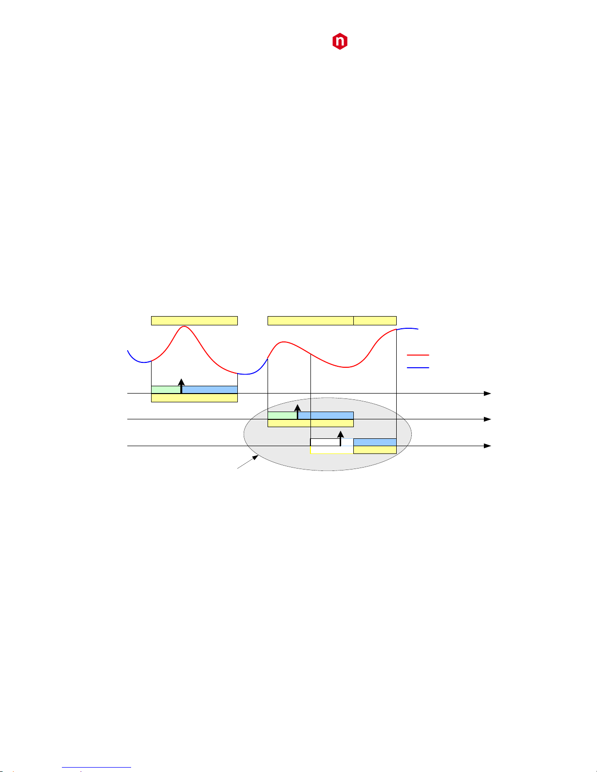
TRIGGER
PRE POST
ACQUISITION WINDOW
Recorded
Not Recorded
Overlapping Triggers
EVENT n EVENT n+1 EVENT n+2
Fig. 9.8: Trigger overlap
A trigger can be refused for the following causes:
- Acquisition is not active.
- Memory is FULL and therefore there are no available buffers.
- The required number of samples for building the pre-trigger of the event is not reached yet; this happens
typically as the trigger occurs too early either with respect to the RUN Acquisition command (see §
Acquisition Run/Stop) or with respect to a buffer emptying after a Memory FULL status (see § Acquisition
Synchronization).
- The trigger overlaps the previous one and the board is not enabled for accepting overlapped triggers.
As a trigger is refused, the current buffer is not frozen and the acquisition continues writing on it. The EVENT COUNTER
can be programmed in order to be either incremented or not. If this function is enabled, the EVENT COUNTER value
identifies the number of the triggers sent (but the event number sequence is lost); if the function is not enabled, the
EVENT COUNTER value coincides with the sequence of buffers saved and readout.

CAEN
Electronic Instrumentation
UM3148 – DT5730/DT5725 User Manual rev. 2
28
Multi-Event Memory Organization
Each channel of the DT5730/DT5725 features a SRAM memory to store the acquired events. The memory size for the
event storage is 640 kS/ch or 5.12 MS/s, according to the board version (see Tab. 1.1), and it can be divided in a
programmable number of buffers, Nb (N
b
from 1 up to 1024), by register address 0x800C, as described in Tab. 9.1
below.
Register Value
Buffer Number
(Nb)
Size of one Buffer (Samples)
SRAM 640 kS/ch⁽*⁾
SRAM 5.12 MS/ch⁽*⁾
0x00
1
640k - 10
5.12M - 10
0x01
2
320k - 10
2.56M - 10
0x02
4
160k - 10
1.28M - 10
0x03
8
80k - 10
640k - 10
0x04
16
40k - 10
320k - 10
0x05
32
20k - 10
160k - 10
0x06
64
10k - 10
80k - 10
0x07
128
5k - 10
40k - 10
0x08
256
2560 - 10
20k - 10
0x09
512
1280 - 10
10k - 10
0x0A
1024
640 - 10
5120 - 10
Tab. 9.1: Buffer Organization
Having 640 kS memory size as reference, this means that each buffer contains 640k/Nb samples (e.g. Nb = 1024 means
640 samples in each buffer).
⁽*⁾IMPORTANT: For AMC FPGA firmware release < 0.2, the Size of one Buffer related to each Buffer Number must be
intended as the number of the samples in Tab. 9.1. without decreasing by 10 samples.
Custom Sized Events
In case an event size minor than the buffer size is needed, the user can set the value N
LOC
at register address 0x8020;
the event is so forced to be made by 10*N
LOC
samples. Setting NLOC = 0, the custom size is disabled. The value of N
LOC
must be set in order that the relevant number of samples does not exceed the buffer size and it mustn’t be modified
while the acquisition is running.
Note: Even using the custom size setting, the number of buffers and the buffer size are not affected by N
LOC
, but they
are still determined by Nb.
The concepts of buffer organization and custom size directly affect the width of the acquisition window (i.e.
number of the digitized waveform samples per event). The Record Length parameter defined in CAEN
software (such as WaveDump and CAENScope introduced in § 11) and the Set/GetRecordLength() function
of the CAENDigitizer library (refer to [RD5] ) rely on these concepts.

CAEN
Electronic Instrumentation
UM3148 – DT5730/DT5725 User Manual rev. 2
29
Event Structure
The event can be readout via Optical Link or USB; data format is 32-bit long word (see Tab. 9.3)
An event is structured in:
• Header (four 32-bit words)
• Data (variable size and format)
Header consists in 4 words including the following information:
• EVENT SIZE (Bit[27:0] of 1
st
header word) = It is the size of the event (number of 32-bit long words);
• BOARD FAIL FLAG (Bit[26] of 2
nd
header word) = Implemented from ROC FPGA firmware revision 4.5 on
(reserved otherwise), this bit is set to “1” in consequence of a hardware problem (e.g. PLL unlocking or overtemperature condition). The user can collect more information about the cause by reading at register address
0x8104 and contact CAEN Support Service if necessary (see § 14);
• Bit[24] (2
nd
header word) = This bit identifies the event format; it is reserved and must be 0;
• Bit[23:8] (2
nd
header word) = Starting from revision 4.6 of the ROC FPGA firmware, these 16 bits can be
programmed to provide different trigger information according to the setting of the bits[22:21] at register
address 0x811C (Tab. 9.2).
Note: for ROC FPGA firmware revisions lower than 4.6. these bits are reserved.
REGISTER 0x811C
Bits[22:21]
FUNCTIONAL
DESCRIPTION
Bit[23:8]
(16 bits in the2nd header word)
00
(default)
Not used
Must be 0
01
Event Trigger Source
Indicates the trigger source causing the
event acquisition:
Bits[23:19] = 0000
Bit[18] = Software Trigger
Bit[17] = External Trigger
Bit[16] = 0
Bits[11:8] = Trigger requests from the
couple of channels (refer to § Self-Trigger)
10
Extended Trigger Time Tag
(ETTT)
A 48-bit Trigger Time Tag (ETTT)
information is configured, where Bits[23:8]
contributes as the 16 most significant bits
together to the 32-bit TTT field (4th header
word).
Note: in the 48-bit TTT, the overflow bit is
not provided.
11
Not used
reserved
Tab. 9.2: TRG OPTIONS configuration table
• CHANNEL MASK (Bit[7:0] of 2
nd
header word) = It is the mask of the channels participating in the event. This
information must be used by the software to acknowledge which channel the samples are coming from.
• EVENT COUNTER (Bit[23:0] of 3
rd
header word) = This is the trigger counter; it can count either accepted
triggers only, or all triggers.

CAEN
Electronic Instrumentation
UM3148 – DT5730/DT5725 User Manual rev. 2
30
• TRIGGER TIME TAG (Bit[31:0] of 4
th
header word) = It is the 31-bit Trigger Time Tag information (31-bit counter
and 32nd bit as roll over flag), which is the trigger time reference. If the ETTT option is enabled, then this field
becomes the 32 less significant bits of the extended 48-bit trigger time tag information in addition to the 16 bits
(MSB) of the TRG OPTIONS field (2nd event word). Note that, in the ETTT case, the roll over flag is no more
provided. The trigger time tag is reset either as the acquisition starts or via front panel signal on GPI connector,
and increments with 125-MHz frequency (every 4 ADC clock cycles in case of DT5730 or 2 ADC clock cycles with
DT5725). The trigger time tag value is read at half this frequency (62.5 MHz). So, the trigger time tag
specifications result in 16 ns resolution and 17 s range(i.e. 8 ns*(231-1)), which can be extended to 625 h (i.e. 8
ns*(248-1)) by the Extended Trigger Time Tag option.
Data are the samples from the enabled channels. Data from masked channels are not read.
Event Format Example
Tab. 9.3 shows the event data format of DT5730/DT5725 when all the 8 channels are enabled. The structure is
described in § Event Structure.
31 30 29 28 27 262524 23 22 21 20 19 18 17 16 15 14 13 12 11 10 9 8 7 6 5 4 3 2 1 0
EVENT SIZE
TRIGGER TIME TAG
101 0
RES.
EVENT COUNTER
SAMPLE [1] – CH[0] SAMPLE [0] – CH[0]
SAMPLE [3] – CH[0] SAMPLE [2] – CH[0]
SAMPLE [N-1] – CH[0] SAMPLE [N-2] – CH[0]
SAMPLE [1] – CH[1] SAMPLE [0] – CH[1]
SAMPLE [3] – CH[1] SAMPLE [2] – CH[1]
SAMPLE [N-1] – CH[1] SAMPLE [N-2] – CH[1]
HEADER DATA CH0 DATA CH1
SAMPLE [1] – CH[7] SAMPLE [0] – CH[7]
SAMPLE [3] – CH[7] SAMPLE [2] – CH[7]
SAMPLE [N-1] – CH[7] SAMPLE [N-2] – CH[7]
DATA CH7
BOARD-ID
0 00 0
0 0
0 0
0 0
0 0
0 0
0 0
0 0
0 0
0 0
0 0
0 0
0 0
0 0
0 0
0 0
0 0
0 0
PATTERN CHANNEL MASK [7:0]
RESERVED
RESERVED BF
RESERVED / TRG OPTIONS
RES.
0
Tab. 9.3: Event Format Example

CAEN
Electronic Instrumentation
UM3148 – DT5730/DT5725 User Manual rev. 2
31
Acquisition Synchronization
Each channel of the digitizer is provided with a SRAM memory that can be organized in a programmable number Nb of
circular buffers (Nb = [1:1024], see Tab. 9.1). When the trigger occurs, the FPGA writes further a programmable number
of samples for the post-trigger and freezes the buffer, so that the stored data can be read via USB or Optical Link. The
acquisition can continue without dead-time in a new buffer.
When all buffers are filled, the board is considered FULL: no trigger is accepted and the acquisition stops (i.e. the
samples coming from the ADC are not written into the memory, so they are lost). As soon as at least one buffer is read
out, the board exits the FULL condition and acquisition restarts.
Note: When the acquisition restarts, no trigger is accepted until at least the entire buffer is written. This means that
the dead time is extended for a certain time (depending on the size of the acquisition window) after the board exits
the FULL condition.
A way to eliminate this extra dead time is by setting bit[5] = 1 at register address 0x8100. The board is so programmed
to enter the FULL condition when N-1 buffers are written: no trigger is then accepted, but samples writing continues in
the last available buffer. As soon as one buffer is readout and becomes free, the boards exits the FULL condition and
can immediately accept a new trigger. This way, the FULL reflects the BUSY condition of the board (i.e. inability to
accept triggers); if required, the BUSY signal can be provided out on the digitizer front panel through the GPO LEMO
connector (bit[20], bits[19:18] and bits[17:16] at register address 0x811C).
Note: when bit[5] = 1, the minimum number of circular buffers to be programmed is N = 2.
In some cases, the BUSY propagation from the digitizer to other parts of the system has some latency and it can
happen that one or more triggers occur while the digitizer is already FULL and unable to accept those triggers. This
condition causes event loss and it is particularly unsuitable when there are multiple digitizers running synchronously,
because the triggers accepted by one board and not by other boards cause event misalignment.
In this cases, it is possible to program the BUSY signal to be asserted when the digitizer is close to FULL condition, but it
has still some free buffers (Almost FULL condition). In this mode, the digitizer remains able to accept some more
triggers even after the BUSY assertion and the system can tolerate a delay in the inhibit of the trigger generation.
When the Almost FULL condition is enabled by setting the Almost FULL level (register address 0x816C) to X, the BUSY
signal is asserted as soon as X buffers are filled, although the board still goes FULL (and rejects triggers) when the
number of filled buffers is N or N-1, depending on bit[5] at register address 0x8100 as described above.
It is possible to provide the BUSY signal on the digitizer front panel GPO output (bit[20], bits[19:18] and bits[17:16] at
register address 0x811C are involved).

CAEN
Electronic Instrumentation
UM3148 – DT5730/DT5725 User Manual rev. 2
32
Trigger Management
According to the default firmware operating, all the channels in a board share the same trigger (board common
trigger), so they acquire an event simultaneously and in the same way (a determined number of samples according to
buffer organization and custom size settings, and position with respect to the trigger given by the post-trigger).
Note: For the trigger management in the DPP firmware operating, please refer to [RD9] and [RD10].
The generation of a common acquisition trigger is based on different trigger sources (configurable at register address
0x810C):
• Software trigger
• External trigger
• Self-trigger
• Coincidence
TRG IN
Enable Mask
x4
COMMON TRIGGER
SW TRG
GPO
(TRG OUT)
TRG_REQ [3:0]
D Q
SCLK
Acquisition
Logic
Memory
Buffers
Local Bus
Interface
Mother Board
x4
4
4
ADC
ADC
CH0
CH1
TRG_REQ [0]
SELF-TRIG. SET.
OVTHR PULSE
SELF-TRIG. SET.
PULSEOVTHR
AND
ONLY 0
ONLY 1
OR
Mezzanine
4
4
Fig. 9.9: Block Diagram of the trigger management
Software Trigger
Software triggers are internally produced via a software command (write access at register address 0x8108) through
USB or Optical Link.
External Trigger
A TTL or NIM external signal can be provided in the front panel TRG-IN connector (configurable at register address
0x811C). If the external trigger is not synchronized with the internal clock, a 1-clock period jitter occurs.

CAEN
Electronic Instrumentation
UM3148 – DT5730/DT5725 User Manual rev. 2
33
Self-Trigger
Each channel is able to generate a self-trigger signal when the digitized input pulse exceeds a configurable threshold
(register address 0x1n60). The self-triggers of each couple of adjacent channels are then processed to provide out a
single trigger request. The trigger requests are propagated to the central trigger logic where they are ORed to produce
the board common trigger, which is finally distributed back to all channels causing the event acquisition (see Fig. 9.9).
Fig. 9.10 schematizes the self-trigger and trigger request logic having the channel 0 and channel 1 couple as an
example.
CH0
CH1
PULSE
OVTHR
Bits[1:0] of 0x1084
PULSE
OVTHR
SELF_TRG [0]
SELF_TRG [1]
AND
ONLY 0
ONLY 1
OR
Bit[2] of 0x1084
TRG_REQ [0]
Fig. 9.10: Self Trigger and Trigger Request logic for Ch0 and Ch1 couple. A single trigger request signal is generated.
The FPGA, by register address 0x1n84, can be programmed in order the self-trigger to be:
▪ an over/under-threshold signal (see Fig. 9.11). This signal can be programmed to be active (i.e. “1”) as long as
the input pulse is over the threshold or under the threshold (depending on the trigger polarity bit at register
address 0x8000).
CH0 IN
THRESHOLD
over-threshold signal [0]
under-threshold signal [0]
Fig. 9.11: Channel over/under threshold signal

CAEN
Electronic Instrumentation
UM3148 – DT5730/DT5725 User Manual rev. 2
34
▪ a pulse of configurable width (see Fig. 9.12). The width parameter can be set at register address 0x1n70.
CH0 IN
THRESHOLD
pulse [0]
WIDTH
Fig. 9.12: Channel pulse signal
The FPGA, by register address 0x1n84, can be programmed in order the trigger request for a couple of adjacent
channels to be the
AND,
ONLY CH(n),
ONLY CH(n+1),
OR
of the relevant self-trigger signals (see Fig. 9.10).
Default Conditions: by default, the FPGA is programmed so that the trigger request is the OR of two pulses of 4nswidth.
Note: the above described configurability of both the self-trigger logic and the trigger request logic are supported only
by AMC FPGA firmware releases > 0.1.
Previous firmware don’t implement the register address 0x1n84 as well as the 0x1n70, the self-trigger is intended only
as the over/under threshold signal and a trigger request is intended only as the OR of the self-triggers couple.

CAEN
Electronic Instrumentation
UM3148 – DT5730/DT5725 User Manual rev. 2
35
Trigger Coincidence Level
Operating with the default firmware, the acquisition trigger is a board common trigger. This common trigger allows the
coincidence acquisition mode to be performed through the Majority operation.
Note: From AMC FPGA firmware release > 0.1, it is possible to program the self-trigger logic as described in § Self-
Trigger.
Enabling the coincidences is possible by writing at register address 0x810C:
- Bits[3:0] enable the trigger request signals to participate in the coincidence;
- Bits[23:20] set the coincidence window (T
TVAW
) linearly in steps of the Trigger clock (8 ns);
- Bits[26:24] set the Majority (i.e. Coincidence) level; the coincidence takes place when:
Number of enabled trigger requests > Majority level
Supposing bits[3:0] = FF (i.e. all the 4 trigger request are enabled) and bits[26:24] = 01 (i.e. Majority level = 1), a board
common trigger is issued whenever at least two of the enabled trigger requests are in coincidence within the
programmed T
TVAW
.
The Majority level must be smaller than the number of trigger requests enabled via bits[3:0] mask. By default,
bits[26:24] = 00 (i.e. Majority level = 0), which means the coincidence acquisition mode is disabled and the T
TVAW
is
meaningless. In this case, the board common trigger is simple OR of the signals from the enabled channels pairs.

CAEN
Electronic Instrumentation
UM3148 – DT5730/DT5725 User Manual rev. 2
36
Fig. 9.13 and Fig. 9.14 show the trigger management in case the coincidences are disabled
CH0 THRESHOLD
CH0 (enabled) IN
Over-threshold signal [CH0]
CH1 THRESHOLD
CH1(enabled) IN
Over-threshold signal [CH1]
TRG_REQ [0]
MEZZANINE
CH2 THRESHOLD
CH2 (enabled) IN
Over-threshold signal [CH2]
CH3 THRESHOLD
CH3(enabled) IN
Over-threshold signal [CH3]
TRG_REQ [1]
Fig. 9.13: Trigger request management at mezzanine level with Majority level = 0
TRG_REQ [0]
MOTHERBOARD
TRG_REQ [1]
ORed signal
COMMON TRIGGER
(Maj. Lev. = 0)
Fig. 9.14: Trigger request management at motherboard level with Majority level = 0

CAEN
Electronic Instrumentation
UM3148 – DT5730/DT5725 User Manual rev. 2
37
Fig. 9.15 and shows the trigger management in case the coincidences are enabled with Majority level = 1 and T
TVAW
is a
value different from 0. In order to simplify the description, CH1 and CH3 channels are considered disabled, so that the
relevant trigger requests are the over-threshold signals from CH0 and CH1.
CH2 THRESHOLD
TRG_REQ [0]
TRG_REQ [1]
CH0(enabled) IN
CH0 THRESHOLD
TRIGGER
(Maj.lev = 1)
CH2(enabled) IN
ORed signal
TTVAW
MEZZANINE
MOTHERBOARD
Fig. 9.15: Trigger request relationship with Majority level = 1 and T
TVAW
≠ 0
Note: with respect to the position where the common trigger is generated, the portion of input signal stored depends
on the programmed length of the acquisition window and on the post trigger setting.

CAEN
Electronic Instrumentation
UM3148 – DT5730/DT5725 User Manual rev. 2
38
Fig. 9.16 shows the trigger management in case the coincidences are enabled with Majority level = 1 and T
TVAW
= 0 (i.e.
1 clock cycle). In order to simplify the description, CH1 and CH3 channels are considered disabled, so that the relevant
trigger requests are the over-threshold signals from CH0 and CH1.
CH2 THRESHOLD
TRG_REQ [0]
TRG_REQ [1]
CH0(enabled) IN
CH0 THRESHOLD
TRIGGER
(Maj.lev = 1)
CH2(enabled) IN
ORed signal
TTVAW
MEZZANINE
MOTHERBOARD
Fig. 9.16: Trigger request relationship with Majority level = 1 and T
TVAW
= 0
In this case, the common trigger is issued if at least two of the enabled trigger requests are instantaneously in
coincidence (no TTVAW is waited).
Note: a practical example of making coincidences with the digitizer in the standard operating is detailed in [RD11].

CAEN
Electronic Instrumentation
UM3148 – DT5730/DT5725 User Manual rev. 2
39
Trigger Distribution
As described in § Trigger Management, the OR of all the enabled trigger sources, synchronized with the internal clock,
becomes the common trigger of the board that is fed in parallel to all channels, consequently provoking the capture of
an event. By default, only the Software Trigger and the External Trigger participate in the common acquisition trigger
(refer to the red path on top of Fig. 9.17).
A Trigger Out signal is also generated on the relevant front panel GPO connector (NIM or TTL), and allows to extend the
trigger signal to other boards. Thanks to its configurability (see Fig. 9.17), GPO can propagate out:
- the OR of all the enabled trigger sources (only the Software Trigger is provided by default, as in the red
path of Fig. 9.17);
- the OR, AND or MAJORITY exclusively of the channel trigger requests.
TRG_REQ[3:0]
GPO
0x8110
Bits[9:8]
00
01
10
TO THE CHANNELS
COMMON ACQUISITON TRIGGER
0x811C
Bits[17:16]
3
3
00
01
MB PROBES
10
PB PROBES
11
GPI
3
SW TRG
EXT TRG
MASK 1
0x810C
Bits[3:0]
MASK 4
0x8110
Bits[3:0]
OR
AND
MAJORITY
OR
MASK 2
MASK 3
0x810C
Bits[31:30]
0x8110
Bits[31:30]
SW TRG
EXT TRG
OR
TRG SOURCES
0x8110
Bits[12:10]
EXT TRG
SW TRG
Fig. 9.17: Trigger configuration on GPO front panel output connector
The registers involved in the GPO programming are:
- Register address 0x8110;
- Register address 0x811C.
Note: Refer to [RD2] for registers complete description.

CAEN
Electronic Instrumentation
UM3148 – DT5730/DT5725 User Manual rev. 2
40
Example
For instance, it could be required to start the acquisition on all the channels of a multi-board system as soon as one of
the channels of a board (board “n”) crosses its threshold. Trigger Out signal is then fed to an external Fan Out logic
unit; the obtained signal has then to be provided to the external trigger input TRG-IN of all the boards in the system
(including the board which generated the Trigger Out signal). In this case, the programming steps to perform are
following described:
1. Register 0x8110 on board “n”:
- Enable the desired trigger request as Trigger Out signal on board “n” (by bits[3:0] mask);
- Disable Software Trigger and External Trigger as Trigger Out signal on board “n” (bits[31:30] = 00);
- Set Trigger Out signal as the OR of the enabled trigger requests on board “n” (bits[9:8] = 00).
2. Register 0x811C on board “n”:
- Configure the digitizer to propagates on GPO the internal trigger sources according to the 0x8110
settings (i.e. the enabled trigger request, in the specific case) on board “n” (bits[17:16] = 00).
3. Register 0x810C on all the boards in the system (including board “n”):
- Enable External Trigger to participate in the board’s common acquisition trigger, disable Software
Trigger and the Trigger Requests from the channels (bits[31:30] = 01; bits[3:0] = 0000).

CAEN
Electronic Instrumentation
UM3148 – DT5730/DT5725 User Manual rev. 2
41
Reset, Clear and Default Configuration
Global Reset
Global Reset is performed at power-on of the module or via software by write access at register address 0xEF24
(whatever 32-bit value can be written). It allows to clear the data off the Output Buffer, the event counter and
performs a FPGAs global reset, which restores the FPGAs to the default configuration. It initializes all counters to their
initial state and clears all detected error conditions.
Memory Reset
The Memory Reset clears the data off the Output Buffer.
The Memory Reset can be forwarded via a write access at register address 0xEF28 (whatever 32-bit value can be
written).
Timer Reset
The Timer Reset allows to initialize the timer which allows to tag an event. The Timer Reset can be forwarded with a
pulse sent to the front panel GPI input (leading edge sensitive).

CAEN
Electronic Instrumentation
UM3148 – DT5730/DT5725 User Manual rev. 2
42
Data Transfer Capabilities
DT5730 and DT5725 feature a Multi-Event digital memory per channel, configurable by the user to be divided into 1 up
to 1024 buffers, as detailed in § Multi-Event Memory Organization. Once they are written in the memory, the events
become available for readout via USB or Optical Link. During the memory readout, the board can store other events
(independently from the readout) on the available free buffers. The acquisition process is so “dead timeless” until the
memory becomes full (see § Acquisition Synchronization).
The events are readout sequentially and completely, starting from the Header of the first available event, followed by
the samples of the enabled channels (from 0 to 7) as reported in Tab. 9.3. Once an event is completed, the relevant
memory buffer becomes free and ready to be written again (old data are lost). After the last word in an event, the first
word (Header) of the subsequent event is readout. It is not possible to readout an event partially.
The size of the event (EVENT SIZE) is configurable and depends on register addresses 0x8020 and 0x800C, as well as on
the number of enabled channels.
Block Transfers
The Block Transfer readout mode allows to read N complete events sequentially, where N is set at register address
0xEF1C, or by using the SetMaxNumEventsBLT function of the CAENDigitizer library (consult [RD5] at p. 19).
When developing programs, the readout process can be implemented on different basis :
• Using Interrupts: as soon as the programmed number of events is available for readout, the board sends an
interrupt to the PC over the optical communication link (not supported by USB).
• Using Polling (interrupts disabled): by performing periodic read accesses to a specific register of the board it is
possible to know the number of events present in the board and perform a BLT read of the specific size to read
them out.
• Using Continuous Read (interrupts disabled): continuous data read of the maximum allowed size (e.g. total
memory size) is performed by the software without polling the board. The actual size of the block read is
determined by the board that terminates the BLT access at the end of the data, according to the configuration
of register address 0xEF1C, or the library function SetMaxNumEventsBLT mentioned above. If the board is
empty, the BLT access is immediately terminated and the “Read Block” function will return 0 bytes (it is the
ReadData function in the CAENDigitizer Library, refer to [RD5]).
Whatever the method from above, it is suggested to ask the board for the maximum of the events per block being set.
Furthermore, the greater this maximum, the greater the readout efficiency, despite of a greater memory allocation
required on the host station side that is actually not a real drawback, considering the features of the personal
computers available on the market.
Note: Involved registers and library functions are detailed respectively in [RD2] and [RD5].
Single Data Transfer
This mode allows to readout a word per time, from the header (actually 4 words) of the first available event, followed
by all the words until the end of the event, then the second event is transferred. The exact sequence of the transferred
words is shown in § Event Structure.
It is suggested, after the 1st word is transferred, to check the EVENT SIZE information and then do as many cycles as
necessary (actually EVENT SIZE -1) in order to read completely the event.

CAEN
Electronic Instrumentation
UM3148 – DT5730/DT5725 User Manual rev. 2
43
Optical Link and USB Access
The board houses a USB2.0 compliant port, providing a transfer rate up to 30 MB/s, and a daisy chainable Optical Link
(communication path which uses optical fiber cables as physical transmission line) providing transfer rate up to 80
MB/s. The latter allows to connect up to 8 DT5730/DT5725 boards to a single A2818 PCI Optical Link Controller or up to
32 boards to a single A3818 PCIe Optical Link Controller. Detailed information on CAEN PCI/PCIe Controllers can be find
at www.caen.it:
Home / Products / Modular Pulse Processing Electronics / PCI/PCIe / Optical Controllers
The parameters for read/write accesses via optical link are Address Modifier, Base Address, data Width, etc.; wrong
parameter settings cause Bus Error.
Bit[3] at register address 0xEF00 allows to enable the module to broadcast an interrupt request on the Optical Link; the
enabled Optical Link Controllers propagate the interrupt on the PCI bus as a request from the Optical Link is sensed.
Interrupts can also be managed at the CAENDigitizer library level (see “Interrupt Configuration” in [RD5]).

CAEN
Electronic Instrumentation
UM3148 – DT5730/DT5725 User Manual rev. 2
44
10 Drivers & Libraries
Drivers
In order to interface with the DT5730/DT5725, CAEN provides the drivers for all the different types of physical
communication channels featured by the board and compliant with Windows and Linux OS:
• USB 2.0 Drivers are downloadable on CAEN website (www.caen.it) in the “Software/Firmware” tab at the
DT5730 and DT5725 web pages (login required).
Note: For Microsoft Windows OS, the USB driver installation is detailed in [RD3].
• Optical Link Drivers are managed by the A2818 PCI card or the A3818 PCIe card. The driver installation
package is available on CAEN website in the “Software/Firmware” area at the A2818 or A3818 page (login
required)
Note: For the installation of the Optical Link driver, refer to the User Manual of the specific Controller.
Libraries
CAEN libraries are a set of middleware software required by CAEN software tools for a correct functioning. These
libraries, including also demo and example programs, represent a powerful base for users who want to develop
customized applications for the digitizer control (communication, configuration, readout, etc.):
• CAENVMELib is a set of ANSI C functions which permit a user program to use and configure the CAEN Bridges
and Controllers V1718/VX1718 (VME-USB2.0 Bridge), V2718/VX2718 (VME-PCI/PCIe Optical Link Bridge),
A2818/A3818 (PCI/PCIe-CONET Controller).
The CAENVMElib installation package is available on CAEN website in the ‘Download’ area at the
CAENVMELib Library page.
• CAENComm library manages the communication at low level (read and write access). The purpose of the
CAENComm is to implement a common interface to the higher software layers, masking the details of the
physical channel and its protocol, thus making the libraries and applications that rely on the CAENComm
independent from the physical layer. Moreover, the CAENComm is based in turn on CAENVMElib and it
requires the CAENVMELib library (access to the VME bus) even in the cases where the VME is not used. This
is the reason why CAENVMELib has to be already installed on your PC before installing the CAENComm.
The CAENComm installation package is available on CAEN website in the ‘Download’ area at the CAENComm
Library page.
• CAENDigitizer is a library of functions designed specifically for the Digitizer family and it supports also the
boards running the DPP firmware. The CAENDigitizer library is based on the CAENComm which is based on
CAENVMELib, as said above. For this reason, the CAENVMELib and CAENComm libraries must be already
installed on the host PC before installing the CAENDigitizer.
The CAENDigitizer installation package is available on CAEN website in the ‘Download’ area at the
CAENDigitizer Library page.

CAEN
Electronic Instrumentation
UM3148 – DT5730/DT5725 User Manual rev. 2
45
The CAENComm (and so the CAENDigitizer) supports the following communication channels:
PC → USB → DT5730/DT5725
PC → PCI (A2818) → CONET → DT5730/DT5725
PC → PCIe (A3818) → CONET → DT5730/DT5725
CONET
2
(
Optical Link
)
A2818 A3818
CAEN SW Tools
USB 2.0
User’s own SW
DT5730/DT5725
CAENComm
CAENDigitizer Library
A2818 driver A3818 driver
USB driver
PCI
PCIe
Fig. 10.1: Required libraries and drivers
If required to be installed apart by the user (see § 11), CAEN Libraries are available for download on CAEN web site
(www.caen.it) in the “Download” tab at the library web page:
Home / Products / Firmware/Software / Digitizer Software / Software Libraries / <CAEN Library>
Install first CAENVMELib, then CAENComm library, finally CAENDigitizer library.

CAEN
Electronic Instrumentation
UM3148 – DT5730/DT5725 User Manual rev. 2
46
11 Software Tools
CAEN provides software tools to interface the DT5730/DT5725, which are available for free download on www.caen.it
at:
Home / Products / Firmware/Software / Digitizer Software
CAENUpgrader
CAENUpgrader is a free software composed of command line tools together with a Java Graphical User Interface.
Specifically for the DT5730/DT5725, CAENUpgrader allows in few easy steps to:
• Upload different firmware versions on the board
• Select which copy of the stored firmware must be loaded at power-on
• Read the firmware release of the board and the bridge (when used)
• Manage the firmware license, in case of pay firmware
• Upgrade the internal PLL
• Get the Board Info file, useful in case of support
CAENUpgrader can operate with Windows and Linux, 32 and 64-bit OSs.
The program relies on the CAENComm and CAENVMELib libraries (see § 10) and requires third-party Java SE6 (or later)
to be installed.
Note: Windows version of CAENUpgrader is stand-alone (the required libraries are installed locally with the program),
while the version for Linux needs the required libraries to be previously installed by the user.
Fig. 11.1: CAENUpgrader Graphical User Interface
CAENUpgrader installation package can be downloaded on CAEN web site (login required) at:
Home / Products / Firmware/Software / Digitizer Software / Configuration Tools / CAENUpgrader
The reference document for installation instructions and program detailed description is [RD1], downloadable at the
same page above, in the Documentation tab.

CAEN
Electronic Instrumentation
UM3148 – DT5730/DT5725 User Manual rev. 2
47
CAENComm Demo
CAENComm Demo is a simple program developed in C/C++ source code and provided both with Java and LabVIEW GUI
interface. The demo mainly allows for a full board configuration at low level by direct read/write access to the registers
and may be used as a debug instrument.
Fig. 11.2: CAENComm Demo Java and LabVIEW graphical interface
CAENComm Demo can operate with Windows OSs, 32 and 64-bit. It requires CAENComm and CAEVMElib libraries as
additional software to be installed (see § 10).
The Demo is included in the CAENComm library installation Windows package, which can be downloaded on CAEN web
site (login required) at:
Home / Products / Firmware/Software / Digitizer Software / Software Libraries / CAENComm Library

CAEN
Electronic Instrumentation
UM3148 – DT5730/DT5725 User Manual rev. 2
48
CAEN WAVEDump
WaveDump is a basic console application, with no graphics, supporting only CAEN digitizers running the default
firmware. It allows the user to program a single board (according to a text configuration file containing a list of
parameters and instructions), to start/stop the acquisition, read the data, display the readout and trigger rate, apply
some post-processing (e.g. FFT and amplitude histogram), save data to a file and also plot the waveforms using Gnuplot
(third-party graphing utility: www.gnuplot.info).
WaveDump is a very helpful example of C code demonstrating the use of libraries and methods for an efficient readout
and data analysis. Thanks to the included source files and the VS project, starting with this demo is strongly
recommended to all those users willing to write the software on their own.
Fig. 11.3: CAEN WaveDump
CAEN WaveDump can operate with Windows and Linux, 32 and 64-bit OSs.
The program relies on the CAENDigitizer, CAENComm and CAENVMELib libraries (see § 10). Linux users are required to
install the third-party Gnuplot.
Note: Windows version of WaveDump is stand-alone (the required libraries are installed locally with the program),
while the version for Linux needs the required libraries to be previously installed by the user.
The installation packages can be downloaded on CAEN web site (login required) at:
Home / Products / Firmware/Software / Digitizer Software / Readout Software / CAEN WaveDump
The reference documents for installation instructions and program detailed description are [RD6] and [RD7],
downloadable at the same page above, in the Documentation tab.

CAEN
Electronic Instrumentation
UM3148 – DT5730/DT5725 User Manual rev. 2
49
CAENScope
In a brand new framework, CAENScope software implements the features of an easy-to-use digital oscilloscope to be
used with CAEN digitizers running the default firmware.
Note: CAENScope support for 725 digitizer family is COMING SOON
CAENScope user friendly interface presents different sections to easily manage the digitizer configuration and plot the
waveforms. Once connected, the program retrieves the digitizer information. Different parameters can be set for the
channels, the trigger and the trace visualization (up to 12 traces can be simultaneously plotted). Signals are recordable
to files in two different formats: Binary (SQLite db) and Text (XML). It is also possible to save and restore the program
settings.
Fig. 11.4: CAENScope main frame
CAENScope can operate with Windows and Linux, 32 and 64-bit OSs. Linux users are required to install the following
packages:
- sharutils;
- libXft;
- libXss (specifically for Debian derived distributions, e.g. Debian, Ubuntu, etc.);
- libXScrnSaver (specifically for RedHat derived distributions, e.g. RHEL, Fedora, Centos, etc.).
The program relies on the CAENDigitizer, CAENComm and CAENVMELib libraries.
Note: Windows version of CAENScope is stand-alone (the required libraries are installed locally with the program),
while the version for Linux needs the required libraries to be previously installed by the user.
The installation packages can be downloaded on CAEN web site (login required) at:
Home / Products / Firmware/Software / Digitizer Software / Readout Software / CAENSCOPE
The reference document for installation instructions and program detailed description is [RD8], downloadable at the
same page above, in the Documentation tab.

CAEN
Electronic Instrumentation
UM3148 – DT5730/DT5725 User Manual rev. 2
50
DPP-PSD Control Software
The DT730 and DT5725 can be equipped (on payment) with a special DPP-PSD firmware.
DPP-PSD Control Software is a software interface for configuration, acquisition, data plotting to be used with the
digitizers who can run the DPP-PSD special firmware. It allows the user to set the parameters for the acquisition, to
configure the DPP, to perform the data readout, the histogram collection and the spectrum or waveform plotting and
saving. The program doesn’t feature data analysis, but can be easily interfaced to software tools for offline analysis.
DPP-PSD Control Software is available both for Windows and Linux platforms.
The program relies on the CAENDigitizer, CAENComm and CAENVMELib libraries (see § 10). Third-party Java SE6 (or
later) needs to be installed.
Note: Windows version of DPP-PSD Control Software is stand-alone (the required libraries are installed locally with the
program; only the communication driver must be installed apart by the user), while the version for Linux needs the
required libraries to be already installed apart.
Fig. 11.5: DPP-PSD Control Software: Top – DPP settings Tab and typical 60Co Total Charge Spectrum; Bottom - PSD 2-D Scatter
Plot
The installation package can be downloaded on CAEN web site (www.caen.it) at:
Home / Products / Firmware/Software / Digitizer Software / Readout Software / DPP-PSD Control Software
The reference document for installation instructions and program detailed description is [RD9].

CAEN
Electronic Instrumentation
UM3148 – DT5730/DT5725 User Manual rev. 2
51
MC²Analyzer (MC²A)
MC²Analyzer (MC²A) is a software specifically designed for digitizers running the special DPP-PHA firmware (724, 725
and 730 families) and the Digital MCAs (x780 Dual Digital MCA, x781 Dual/Quad Digital MCA, DT5770).
The software is able to completely control and manage a set of boards acquiring data simultaneously, making therefore
a multi-board system a "Multichannel - Multichannel Analyzer".
MC²A allows the user to set all the relevant DPP-PHA parameters for each acquisition channel (like trigger threshold,
shaping parameters, etc.), handle the communication with the connected boards, run the data acquisition and plot
both waveforms for on-line monitoring of the acquisition and histograms. It can also control the HV power supplies
provided in the x780.
Moreover, it is able to perform advanced mathematical analysis on both the ongoing histograms and collected spectra:
peak search, background subtraction, peak fitting, energy calibration, ROI selection, dead time compensation,
histogram rebin and other features available.
Fig. 11.6: MC²Analyzer (MC²A) software tool
MC²Analyzer is currently available only for Windows platforms. The installation package can be downloaded on CAEN
web site (www.caen.it) at:
Home / Products / Firmware/Software / Digitizer Software / Readout Software
The reference document for installation instructions and program detailed description is [RD10].
Note: Windows version of MC²Analyzer is stand-alone (the required libraries are installed locally with the program;
only the communication driver must be installed apart by the user).

CAEN
Electronic Instrumentation
UM3148 – DT5730/DT5725 User Manual rev. 2
52
12 HW Installation
Power-on Sequence
To power on the board, follow the procedure below:
1. connect the 12V DC power supply to the DT5730/DT5725 through the DC input rear connector;
2. power up the DT5730/DT5725 through the ON/OFF rear switch.
See § Rear Panel to identify the relevant components
Power-on Status
At power-on, the module is in the following status:
• the Output Buffer is cleared;
• registers are set to their default configuration.
After the power-on, the front panel LEDs status is that only the NIM and PLL LOCK remain ON (see Fig. 12.1).
Fig. 12.1: Front panel LEDs status at power ON
AFTER POWER-ON, CAEN RECOMMENDS TO PERFORM THE CHANNEL CALIBRATION AS DESCRIBED AT PAGE 22 IN
ORDER TO ACHIEVE THE BEST DEVICE PERFORMANCE

CAEN
Electronic Instrumentation
UM3148 – DT5730/DT5725 User Manual rev. 2
53
13 Firmware and Upgrades
The board hosts one FPGA on the mainboard and two FPGAs on the mezzanine (i.e. one FPGA per 4 channels). The
channel FPGAs firmware is identical. A unique file is provided that will update all the FPGAs at the same time.
ROC FPGA MAINBOARD FPGA (Readout Controller + VME interface):
FPGA Altera Cyclone EP1C20.
AMC FPGA MEZZANINE FPGA (ADC readout/Memory Controller):
FPGA Altera Cyclone EP4CE30
The firmware is stored onto the on-board FLASH memory. Two copies of the firmware are stored in two different pages
of the FLASH, referred to as Standard (STD) and Backup (BKP). In case of default firmware, the board is delivered
equipped with the same firmware version on both pages.
At power-on, a microcontroller reads the FLASH memory and programs the module automatically loading the first
working firmware copy, that is the STD one by default.
It is possible to upgrade the board firmware via USB or Optical Link by writing the FLASH with the CAENUpgrader
software (see § 11).
IT IS STRONGLY SUGGESTED TO OPERATE THE DIGITIZER UPON THE STD COPY OF THE FIRMWARE. UPGRADES ARE
SO RECOMMENDED ONLY ON THE STD PAGE OF THE FLASH. THE BKP COPY IS TO BE INTENDED ONLY FOR
RECOVERY USAGE. IF BOTH PAGES RESULT CORRUPTED, THE USER WILL NO LONGER BE ABLE TO UPLOAD THE
FIRMWARE VIA USB OR OPTICAL LINK AGAIN AND THE BOARD NEEDS TO BE SENT TO CAEN IN REPAIR!
In case of upgrading failure (e.g. STD FLASH page is corrupted), the user can try to reboot the board: after a power
cycle, the system programs the board automatically from the alternative FLASH page (e.g. BKP FLASH page) if this is not
corrupted as well. The user can so perform a further upgrade attempt on the STD page to restore the firmware copy.
At power-on, if the user cannot communicate with the board, it needs to be sent back to CAEN in repair (see § 14).

CAEN
Electronic Instrumentation
UM3148 – DT5730/DT5725 User Manual rev. 2
54
Default Firmware Upgrade
The DT5730 and DT5725 are delivered running a default firmware to operate the board for waveform recording.
The default firmware updates are available for download on CAEN website (www.caen.it) in the Software/Firmware
tab at the DT5730/DT5725 web pages (login required):
Home / Products / Modular Pulse Processing Electronics / Desktop / Digitizers / DT5730 (or DT5725)
Upgrade Files Description
The programming file has the extension .CFA (CAEN Firmware Archive) and is a sort of archive format file aggregating
all the default firmware files compatible with the same family of digitizers.
CFA and its name follows this general scheme:
x730_revX.Y_W.Z.CFA
x725_revX.Y_W.Z.CFA
where:
• x730 (x725) are all the boards the file is compliant to: DT5730 (DT5725), N6730 (N6725), V1730 (V1725),
VX1730 (VX1725)
• X.Y is the major/minor revision number of the mainboard FPGA
• W.Z is the major/minor revision number of the channel FPGA
DPP Firmware Upgrade
CAEN provides DT5730 and DT5725 with special DPP-PSD and DPP-PHA firmware for Physics Applications. The digitizer
running DPP-PSD firmware becomes a digital replacement of dual gate QDC, discriminator and gate generator. The
digitizer running DPP-PHA firmware becomes a digital replacement of Shaping Amplifier and Peak Sensing ADC (MultiChannel Analyzer) by means of digital trapezoidal filters.
• The DPP-PSD firmware updates are available for download on CAEN website in the Download tab (login
required) at:
Home / Products / Firmware/Software / Digitizer Software / Readout Software / DPP-PSD Control Software
• The DPP-PHA firmware updates are available for download on CAEN website in the Download tab (login
required) at:
Home / Products / Firmware/Software / Digitizer Software / Readout Software / DPP-PHA Control Software
Upgrade File Description
The programming file has the extension .CFA (CAEN Firmware Archive) and is a sort of archive format file aggregating
all the DPP-PSD firmware files compatible with the same family of digitizers
CFA and its name follows this general scheme:
x730_DPP-PSD_rev_X.Y_136.Z.CFA
x725_DPP-PSD_rev_X.Y_136.Z.CFA
x730_DPP-PHA_rev_X.Y_139.Z.CFA
x725_DPP-PHA_rev_X.Y_139.Z.CFA
where the major revision number of the channel FPGA (136 or 139) is fixed for the specific DPP algorithm and digitizer
family. The other fields have the same meaning as in the default firmware file description.
Note: DPP special firmware is a pay firmware requiring a license to be purchased. If not licensed, the firmware can be
loaded but it will run fully functional with a time limitation per power cycle (30 minutes). Details on the license
ordering procedure can be found in [RD1].
Note: if the DPP firmware license is included in the same order of a DT5730 (DT5725), the customer will be delivered
with the digitizer already running the licensed (i.e. unlocked) special firmware. Once unlocked, upgrading the same
kind of DPP firmware requires no further licensing.

CAEN
Electronic Instrumentation
UM3148 – DT5730/DT5725 User Manual rev. 2
55
14 Technical Support
CAEN support services are available for the user by accessing the Support & Services area on CAEN website at
www.caen.it.
Returns and Repairs
Users who need for product(s) return and repair have to fill and send the Product Return Form (PRF) in the Returns and
Repairs area at Home / Support & Services, describing the specific failure. A printed copy of the PRF must also be
included in the package to be shipped.
Contacts for shipping are reported on the website at Home / Contacts.
Technical Support Service
CAEN makes available the technical support of its specialists at the e-mail addresses below:
support.nuclear@caen.it
(for questions about the hardware)
support.computing@caen.it
(for questions about software and libraries)

CAEN
Tools for Discovery
n
Electronic Instrumentation
UM3148 – DT5730/DT5725 User Manual rev. 2
56
CAEN SpA is acknowledged as the only company in the world providing a complete range of High/Low Voltage Power
Supply systems and Front-End/Data Acquisition modules which meet IEEE Standards for Nuclear and Particle Physics.
Extensive Research and Development capabilities have allowed CAEN SpA to play an important, long term role in this field.
Our activities have always been at the forefront of technology, thanks to years of intensive collaborations with the most
important Research Centres of the world. Our products appeal to a wide range of customers including engineers, scientists
and technical professionals who all trust them to help achieve their goals faster and more effectively.
CAEN S.p.A.
CAEN GmbH
CAEN Technologies, Inc.
Via Vetraia, 11
Klingenstraße 108
1140 Bay Street - Suite 2 C
55049 Viareggio
D-42651 Solingen
Staten Island, NY 10305
Italy
Germany
USA
Tel. +39.0584.388.398
Phone +49 (0)212 254 4077
Tel. +1.718.981.0401
Fax +39.0584.388.959
Fax +49 (0)212 25 44079
Fax +1.718.556.9185
info@caen.it
Mobile +49 (0)151 16 548 484
info@caentechnologies.com
www.caen.it
info@caen-de.com
www.caentechnologies.com
www.caen-de.com
CAEN
Tools for Discovery
Electronic Instrumentation
UM3148 - DT5730/DT5725 - User Manual rev. 2 - 10 June 2016
00108-12-DT5730-MUTX
Copyright © CAEN SpA. All rights reserved. Information in this publication supersedes all earlier versions. Specifications subject to change without notice.
 Loading...