

Page 1

CAEN
Tools for Discovery
n
Electronic Instrumentation
User Manual UM6508
DT5495
Desktop Programmable Logic Unit
Rev. 0 - August 2
nd
, 2018
Page 2

Purpose of this Manual
This document contains the full hardware and software description of the DT5495 Desktop Programmable Logic Unit.
Change Document Record
Date
Revision
Changes
August 2nd, 2018
00
Initial release
Symbols, Abbreviated Terms and Notation
AM
Address Modifier
ETH
Ethernet Interface
FPGA
Field Programmable Gate Array
GDG
Gate and Delay Generator
LB
Local Bus
LBM
Local Bus Master
LBS
Local Bus Slave
LED
Light Emitting Diode
MFPGA
Main FPGA
SPI
Serial Peripheral Interface
UFPGA
User FPGA
USB
Universal Serial Bus
Reference Documents
[RD1] GD2512 – CAENUpgrader QuickStart Guide
[RD2] A967 Adapter for P50E – 068S 68 Pin Connectors
[RD3] UM6510 – CAEN PLULib Library User Manual
All documents can be downloaded at: http://www.caen.it/csite/LibrarySearch.jsp
Page 3

CAEN S.p.A.
Via Vetraia, 11 55049 Viareggio (LU) - ITALY
Tel. +39.0584.388.398 Fax +39.0584.388.959
[email protected]
www.caen.it
© CAEN SpA – 2018
Disclaimer
None of the parts of this manual may be reproduced in any form or by any means, electronic, mechanical, recording, or
otherwise, without the prior written permission of CAEN SpA.
The information contained herein has been carefully checked and is believed to be accurate; however, no responsibility
is assumed for inaccuracies. CAEN SpA reserves the right to modify its products specifications without giving any
notice; for up to date information please visit www.caen.it.
MADE IN ITALY: We stress the fact that all the boards are made in Italy because in this globalized world, where getting
the lowest possible price for products sometimes translates into poor pay and working conditions for the people who
make them, at least you know that who made your board was reasonably paid and worked in a safe environment. (this
obviously applies only to the boards marked "MADE IN ITALY", we cannot attest to the manufacturing process of "third
party" boards).
Page 4

CAEN
Electronic Instrumentation
UM6508 – DT5495 User Manual rev. 0
4
Index
Purpose of this Manual ......................................................................................................................................... 2
Change Document Record ................................................................................................................................... 2
Symbols, Abbreviated Terms and Notation ....................................................................................................... 2
Reference Documents ........................................................................................................................................... 2
Index ........................................................................................................................................ 4
List of Figures......................................................................................................................... 5
List of Tables .......................................................................................................................... 5
1 Introduction ..................................................................................................................... 7
2 Block Diagram ................................................................................................................ 9
3 Main Components and Interconnections .................................................................. 10
3.1 USB Interface............................................................................................................................................ 11
3.2 Ethernet Interface ..................................................................................................................................... 11
3.3 Main FPGA ................................................................................................................................................ 11
3.4 User FPGA ................................................................................................................................................ 11
3.5 Gate and Delay Generator ...................................................................................................................... 11
3.6 Clock Distribution ..................................................................................................................................... 11
4 Front Panel Connectors, LEDs and Labels .............................................................. 12
4.1 Front Panel ................................................................................................................................................ 13
4.2 Rear Panel ................................................................................................................................................ 15
5 Technical Specifications ............................................................................................. 17
6 Power Requirements ................................................................................................... 19
7 Getting Started with DT5495 ....................................................................................... 20
7.1 Shipping Content ...................................................................................................................................... 20
7.2 Mezzanine Boards Installation ............................................................................................................... 21
7.3 Front Panel Connector Cabling .............................................................................................................. 22
7.4 Power-on Configuration Sequence ........................................................................................................ 23
Restore Function .............................................................................................................................................................23
8 Communication ............................................................................................................ 24
8.1 Drivers ........................................................................................................................................................ 24
Direct USB Driver Installation ......................................................................................................................................24
8.2 Ethernet Configuration............................................................................................................................. 28
8.3 Web Interface............................................................................................................................................ 30
8.4 Software Tools .......................................................................................................................................... 31
CAENUpgrader.................................................................................................................................................................31
PLULib Library .................................................................................................................................................................34
9 Software Interface ........................................................................................................ 35
9.1 Address Map ............................................................................................................................................. 35
User FPGA Data Access (0x0000-0x0FFF) ................................................................................................................35
User FPGA Register Access (0x1000-0x7FFF) .........................................................................................................35
Configuration ROM (0x8100-0x81FF) .........................................................................................................................36
Configuration and Status Registers (0x8200-0x83FF) ...........................................................................................36
MFPGA Firmware Revision Register ..........................................................................................................................37
Software Reset Register ................................................................................................................................................37
Scratch Register ..............................................................................................................................................................37
Flash Configuration (0x8500-0x8AFF)........................................................................................................................37
Internal Scratch SRAM(0x8C00-0x8FFF) ...................................................................................................................37
10 Firmware Development................................................................................................ 38
10.1 Introduction................................................................................................................................................ 38
10.2 User FPGA I/O ports ................................................................................................................................ 39
10.3 Local Bus Interface .................................................................................................................................. 42
10.4 Gate and Delay Controller ...................................................................................................................... 44
General Description ........................................................................................................................................................44
Register Description .......................................................................................................................................................45
Example Procedures ......................................................................................................................................................46
10.5 Porting V1495 to DT5495 ....................................................................................................................... 47
Page 5

CAEN
Electronic Instrumentation
UM6508 – DT5495 User Manual rev. 0
5
11 Demo Firmware ............................................................................................................ 48
11.1 Introduction................................................................................................................................................ 48
11.2 Demo Structure ........................................................................................................................................ 48
11.3 Demo Setup .............................................................................................................................................. 48
11.4 Gate Pattern Demo Description ............................................................................................................. 49
Introduction ......................................................................................................................................................................49
Register Map ....................................................................................................................................................................49
Register Description .......................................................................................................................................................49
11.5 Pattern Recorder Demo Description ..................................................................................................... 52
Introduction ......................................................................................................................................................................52
Register Map ....................................................................................................................................................................52
Register Description .......................................................................................................................................................52
11.6 DAC Demo Description ........................................................................................................................... 54
Introduction ......................................................................................................................................................................54
Register Map ....................................................................................................................................................................54
Register Description .......................................................................................................................................................54
11.7 Gate and Delay Demo Description ........................................................................................................ 56
Introduction ......................................................................................................................................................................56
Register Map ....................................................................................................................................................................56
Register Description .......................................................................................................................................................56
12 Software Development ................................................................................................ 59
13 CAEN Support ............................................................................................................... 60
13.1 Returns and Repairs ................................................................................................................................ 60
13.2 Technical Support Service ...................................................................................................................... 60
List of Figures
Fig. 2.1: Block diagram ........................................................................................................................................................................9
Fig. 3.1: Main components and interconnections ...........................................................................................................................10
Fig. 3.2: The UFPGA and GDG interface. .......................................................................................................................................11
Fig. 4.1: front (top) and rear (down) panel view .............................................................................................................................12
Fig. 7.1: DT5495 motherboard with mezzanine boards ................................................................................................................21
Fig. 7.2: Multi-pin connector pin assignment ..................................................................................................................................22
Fig. 7.3: CAEN A967 Cable Adapter ................................................................................................................................................22
Fig. 8.1: DT5495 hardware detection ...............................................................................................................................................24
Fig. 8.2: USB driver manual installation: Step1 ..............................................................................................................................25
Fig. 8.3: USB driver manual installation: Step2 ..............................................................................................................................25
Fig. 8.4: USB driver manual installation: Step3 ..............................................................................................................................26
Fig. 8.5: USB driver manual installation: Step4 ..............................................................................................................................26
Fig. 8.6: USB driver manual installation: Step5 ..............................................................................................................................27
Fig. 8.7: The Network and Sharing Center window .......................................................................................................................28
Fig. 8.8: Properties window of the Ethernet network .....................................................................................................................28
Fig. 8.9: Ethernet Properties window” ..............................................................................................................................................29
Fig. 8.10: Properties window of the ”Internet Protocol Version (TPC/IPv4)” ..............................................................................29
Fig. 8.11: Instrument Information page of the DT5495 Web Interface ........................................................................................30
Fig. 8.12: Instrument Information page of the DT5495 Web Interface ........................................................................................30
Fig. 8.13: CAENUpgrader Get Firmware Release menu ..............................................................................................................31
Fig. 8.14: CAENUpgrader MFPGA Upgrade Firmware menu ......................................................................................................32
Fig. 8.15: CAENUpgrader UFPGA flash memory image menu ...................................................................................................33
Fig. 8.16: CAENUpgrader UFPGA Upgrade Firmware menu ......................................................................................................33
Fig. 8.17: CAEN PLULib Demo application prompt .......................................................................................................................34
Fig. 10.1: CAENComm Demo Java and LabVIEW graphical interface .......................................................................................40
Fig. 10.2: Local bus signals at a write access (x8BADF00D is written on register x1800) ......................................................42
Fig. 10.3: Local bus signal at a read access (x8BADF00D is read from register x1800) .........................................................42
Fig. 10.4: Prefetch mechanism .........................................................................................................................................................43
Fig. 10.5: Gate and Delay parameters representation ..................................................................................................................44
List of Tables
Tab. 1.1: Comparison table between V1495 and DT5495 ..............................................................................................................7
Tab. 1.2: Table of models and related items .....................................................................................................................................8
Tab. 5.1: DT5495 specifications table..............................................................................................................................................17
Page 6

CAEN
Electronic Instrumentation
UM6508 – DT5495 User Manual rev. 0
6
Tab. 5.2: A395A Mezzanine specifications table............................................................................................................................17
Tab. 5.3: A395B Mezzanine specifications table............................................................................................................................18
Tab. 5.4: A395C Mezzanine specifications table ...........................................................................................................................18
Tab. 5.5: A395D Mezzanine specifications table ...........................................................................................................................18
Tab. 5.6: A395E Mezzanine specifications table............................................................................................................................18
Tab. 9.1: DT5495 register address map ..........................................................................................................................................35
Tab. 9.2: ROM Address Map of the DT5495 ..................................................................................................................................36
Tab. 9.3: CSR registers .....................................................................................................................................................................36
Tab. 10.1: Clock ports description table ..........................................................................................................................................39
Tab. 10.2: Mainboard Robinson-Nugent connector description table .........................................................................................39
Tab. 10.3: LEMO G ports description table .....................................................................................................................................39
Tab. 10.4: Expansion I/O ports description table ...........................................................................................................................39
Tab. 10.5: A395D mapping................................................................................................................................................................40
Tab. 10.6: LED ports description table ............................................................................................................................................40
Tab. 10.7: Gate and Delay Generator ports description table ......................................................................................................40
Tab. 10.8: Local Bus ports description table ...................................................................................................................................41
Tab. 10.9: Main parameters of the Gate and Delay Generator ....................................................................................................44
Tab. 10.10: Local Bus registers description for the Gate and Delay Generator configuration ................................................45
Page 7

CAEN
Electronic Instrumentation
UM6508 – DT5495 User Manual rev. 0
7
1 Introduction
The DT5495 is a general-purpose programmable FPGA and I/O unit in a compact desktop form factor. The
board is a suitable solution for the implementation of digital functions such as Coincidence, Trigger Logic,
Gate and Delay Generator, Input/Output Register and more.
The programmable architecture is based on the User FPGA (hereafter UFPGA). The UFPGA is directly
interfaced to the front panel I/Os and to an onboard Gate and Delay Generator, that allows to delay and gate
up to 32 signals. A second FPGA, the Main FPGA (hereafter MFPGA), is responsible for USB and Ethernet
interface management. The MFPGA communicates with the UFPGA through an internal local bus.
The presence of three expansion slots interfaced to the UFPGA allows to extend the channel interface of the
DT5495 by adding up to three independent mezzanine boards. Five mezzanine board types are available:
A395A, A395B, A395C, A395D, A395E (see Tab. 1.2). The DT5495 can reach a maximum of 194 I/O channels.
The board can be controlled and programmed through either the Ethernet or the USB interface. The
CAENUpgrader software tool is provided to upload the FPGA firmware, while a dedicated C library is
available to support the custom software development. A rear panel dedicated JTAG connector allows for insystem JTAG configuration and debugging (e.g. using Altera SignalTap).
Simple operations, like retrieving the board information or changing the ethernet settings, can be performed
simply via the Internet or a Local Area Network (LAN) through the web inteface, without need of any control
software but just opening a web browser.
The DT5495 is also available in VME form factor, called V2495, which represents an evolution of CAEN V1495
board. Thanks to several analogies with the V1495 (e.g. the front panel connectors have the same function
and nomenclature with respect to the V1495), users who want to upgrade their system with the DT5495 can
port their firmware already developed for the V1495 just considering few hints (Sect. Porting V1495 to
DT5495).
The following Tab. 1.1 is a comparison table between the two modules.
V1495
DT5495
User FPGA
Altera Cyclone EPI1C20, 20k LEs
Altera Cyclone V GX, 50k LEs
Front Panel I/O
Sections A and B (2 x 68-pin Robinson Nugent connector; 32 input channel each)
Section C (1 x 68-pin Robinson Nugent connector; 32 output channels)
Section G (2 X LEMO connector; input/output channels)
On-board Delay
Generator
4 Delay lines
32 Gate and Delay lines
Local Bus
16-bit 50 MHz parallel interface
VME Bus
Addressing spaces: A24, A32
Data transfer modes: D16, D32, BLT32
Not Supported
USB Interface
Not Supported
USB2.0
ETH Interface
Not Supported
ETHERNET 10/100T
Mezzanine
Boards
A395A, A395B, A395C, A395D, A395E
Tab. 1.1: Comparison table between V1495 and DT5495
Page 8
CAEN
Electronic Instrumentation
UM6508 – DT5495 User Manual rev. 0
8
Tab. 1.2 lists the board models, the firmware and hardware related products as well as the ordering option
information.
Board Models
Description
Product Code
DT5495
Desktop Programmable Logic Unit
WDT5495XAAAA
User Firmware
Description
Product Code
FW2495SC⁽*⁾
Channel Latching Scaler for V2495 and DT5495
WFW2495SCXAA
Accessories
Description
Product Code
A395A
32 LVDS/ECL/PECL input channels
WA395XAAAAAA
A395B
32 LVDS output channels
WA395XBAAAAA
A395C
32 ECL output channels
WA395XCAAAAA
A395D
8 NIM/TTL input/output channels
WA395XDAAAAA
A395E
8 Channel 16Bit ±5V DAC
WA395XEAAAAA
A967
32 Channel Cable Adapter (1x32 to 2x16)
WA967XAAAAAA
Tab. 1.2: Table of models and related items
⁽*⁾ Paid firmware; unlocking license needed. Please, refer to the FW2495SC web page for details.
Page 9

CAEN
Electronic Instrumentation
UM6508 – DT5495 User Manual rev. 0
9
2 Block Diagram
A
B
C
32
32
32
32
32
32
USER
PROGRAMMABLE
FPGA
(UFPGA)
MAIN FPGA
(MFPGA)
16 bit
ETHERNET
LOCAL
BUS
G
Gate and Delay
Generator
D
E
F
USB
32
Fig. 2.1: Block diagram
Page 10
CAEN
Electronic Instrumentation
UM6508 – DT5495 User Manual rev. 0
10
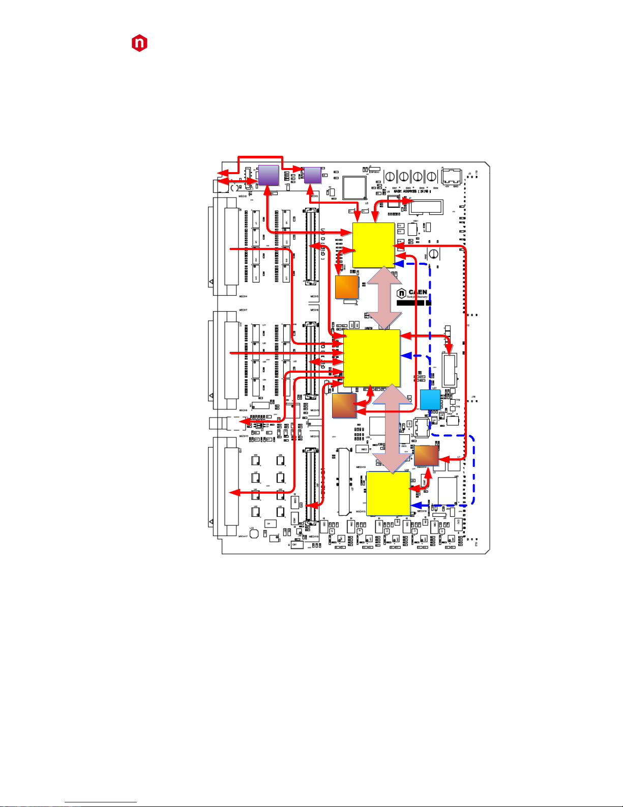
3 Main Components and Interconnections
User
FPGA
(Cyclone V GX)
Main
FPGA
(Cyclone V E)
Gate and Delay
Generator
Local Bus
(16-bit@50MHz)
USB
PHY
FLASH
FLASH
FLASH
A PORT (IN) /
D PORT (IN/OUT)
B PORT (IN) /
E PORT (IN/OUT)
C PORT (OUT) /
F PORT (IN/OUT)
USB
G PORT (IN/OUT)
JTAG
JTAG
USER FW
SELECTOR
50 MHz
50 MHz
50 MHz
AD9520
ETH
ETH
Fig. 3.1: Main components and interconnections
Page 11

CAEN
Electronic Instrumentation
UM6508 – DT5495 User Manual rev. 0
11
3.1 USB Interface
The DT5495 is equipped with a USB2.0 interface. The USB physical layer is managed by a high-speed transceiver
controlled by the Main FPGA.
3.2 Ethernet Interface
In addition to the USB, the DT5495 provides a 10/100T Ethernet interface controlled by the Main FPGA.
3.3 Main FPGA
The MFPGA (Altera Cyclone V E) manages the Ethernet and USB interfaces and the connection with the UFPGA through
a proprietary 16-bit@50 MHz local bus. The MFPGA has a dedicated external flash memory for configuration purposes.
It also pilots the flash memories dedicated to loading the firmware on the UFPGA and on the GDG.
3.4 User FPGA
The User FPGA (Altera Cyclone V GX) manages the I/O peripherals (A/D, B/E, G, C/F ports) and communicates with the
GDG. A dedicated external flash memory can store a set of firmware images to be loaded on the User FPGA. A
dedicated JTAG connector allows to program the UFPGA “on-the-fly” for fast firmware prototyping and debugging.
3.5 Gate and Delay Generator
The DT5495 hosts a Gate and Delay Generator (see Fig. 3.2) able to provide up to 32 gated and delayed signals
(“delayed signals”) triggered by 32 inputs (“start signals”). The gate width and delay value are user programmable. The
GDG is an external component implemented in a Xilinx Spartan-6 FPGA. It is connected through a serial bus (SPI) to the
User FPGA for gate and delay register programming (refer to Sect. Gate and Delay Controller for detailed information).
The GDG configuration is stored in a dedicated flash memory. The GDG firmware cannot be modified by the user.
User FPGA
Gate and Delay
Generator
32
32
Start signals
Delayed signals
Start[i]
Delayed[i]
Td Tg
Fig. 3.2: The UFPGA and GDG interface.
3.6 Clock Distribution
Each FPGA receives the same 50-MHz system clock generated by a common on-board oscillator.
Page 12

CAEN
Electronic Instrumentation
UM6508 – DT5495 User Manual rev. 0
12
4 Front Panel Connectors, LEDs and Labels
USB PORT
&
ACTIVITY LED
CONFIGURATION
LED
‘A’ CONNECTOR
(32-ch input only)
USER CONFIGURATION
LEDs
‘B’ CONNECTOR
(32-ch input only)
‘C’ CONNECTOR
(32-ch output only)
G0, G1 CONNECTORS
(Input/Output selectable)
ETH PORT
‘JTAG’ CONNECTOR
IDENTIFICATION
LABEL
‘RESTORE’
BUTTON
DC IN
CONNECTOR
ON/OFF
SWITCH
Fig. 4.1: front (top) and rear (down) panel view
Page 13

CAEN
Electronic Instrumentation
UM6508 – DT5495 User Manual rev. 0
13
4.1 Front Panel
USB PORT
FUNCTION
MiniUSB connector to
communicate with the DT5495 by
USB link for board configuration
and firmware upgrade.
ELECTRICAL SPECS
N.A.
MECHANICAL SPECS
Series: miniUSB connectors.
Type: SD-54819-026 (B-type).
Manufacturer: Molex Inc.
CABLES
A 1-m USB standard cable is included with
the DT5495 (USB A-type to miniUSB B-type).
USB LED (GREEN): driven by the Main PFGA, this LED lights up if a USB read/write access to the board is performed.
ETHERNET PORT
FUNCTION
Ethernet connector to communicate
with the DT5495 for board
configuration and firmware upgrade.
ELECTRICAL SPECS
10/100T ETHERNET
MECHANICAL SPECS
Series: RJ45 connectors.
Type: GIGABIT MIC3801D-5166.
Manufacturer: Wurt.
CABLES
A 2-m Ethernet cable is included with the
DT5495 (type ASSMANN: AMCSSP60020/R).
A, B, C CONNECTORS
FUNCTION
Motherboard I/O 34+34 pin connectors:
- A/B are inputs
- C is an output
ELECTRICAL SPECS
See Tab. 5.1.
MECHANICAL SPECS
Series: 80-0009-0666-1.
Type: P50E-068-P1-SR1-TG.
Manufacturer: 3M.
CFG LED
FUNCTION
This LED is constantly on when all the
on-board FPGAs are configured by the
application firmware on their relevant
flash memory. The LED blinks if the
MFPGA is in Factory mode.
COLOR
Green.
Page 14

CAEN
Electronic Instrumentation
UM6508 – DT5495 User Manual rev. 0
14
G0, G1 CONNECTORS
FUNCTION
Bidirectional single-ended connectors. Factory
direction is Output. (high impedance state).
External 50Ω termination required when using
the connector as input.
ELECTRICAL SPECS
See Tab. 5.1.
MECHANICAL SPECS
Series: 00 LEMO Connectors.
Type: EPY.00.250.NTN.
Manufacturer: LEMO
0, 1, 2, …, 7 LEDs
FUNCTION
The status of these LEDs is user-programmable
NOTE: when the UFPGA is in Factory mode, odd and even LEDs
alternatively blink.
COLOR
Green.
Page 15
CAEN
Electronic Instrumentation
UM6508 – DT5495 User Manual rev. 0
15
4.2 Rear Panel
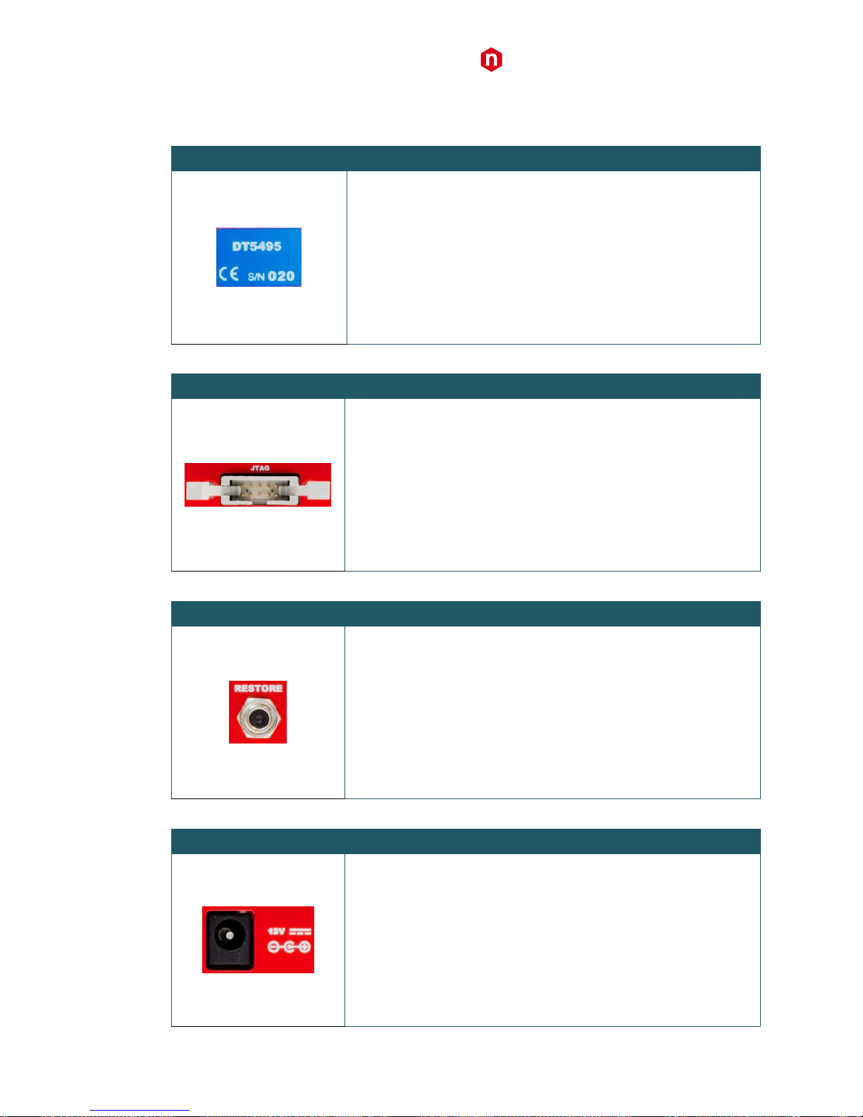
IDENTIFICATION LABEL
A blue label on the Desktop rear panel indicates:
- the model;
- the serial number (S/N);
- the symbol of the CE conformity marking.
JTAG CONNECTOR
FUNCTION
This connector allows for on-the-fly
FPGA programming.
ELECTRICAL SPECS
N.A.
MECHANICAL SPECS
Series: 4600 - panel rectangular
connectors.
Type: 4610-6350.
Manufacturer: 3M.
RESTORE BUTTON
FUNCTION
Restores the default IP address and
forces the module in factory state (see
Sect. Restore Function).
ELECTRICAL SPECS
N.A.
MECHANICAL SPECS
Series: 9000 - momentary pushbutton
switches.
Type: APR9433NA-O.
Manufacturer: Apem.
JTAG CONNECTOR
FUNCTION
Input connector for the DT5495
main power supply from the
external AC/DC adaptor.
ELECTRICAL SPECS
Input voltage: +12 VDC (typ.).
MECHANICAL SPECS
Series: DC power Jacks.
Type: KLDX-0202-A-LT.
Manufacturer: KYCON.
Page 16

CAEN
Electronic Instrumentation
UM6508 – DT5495 User Manual rev. 0
16
ON/OFF SWITCH
FUNCTION
Power switch of the module:
on (I) / off (O)
ELECTRICAL SPECS
N.A.
MECHANICAL SPECS
Series: Power Switches.
Type: Rocker SwitchP (A11131121000)
Manufacturer: Molveno.
Page 17

CAEN
Electronic Instrumentation
UM6508 – DT5495 User Manual rev. 0
17
5 Technical Specifications
DT5495 Motherboard
FORM FACTOR
Desktop module
I/O SECTIONS A and B
Nr. of Channels
32
Direction
Input
Logic
Direct
Signal
Differential LVDS/ECL/PECL
(single ended TTL optional)
Z
diff
: 100 Ω
Extended Common Mode
Input range: -4V to +5V
Fail Safe input feature
Bandwidth
200 MHz
Front Panel Connector
Robinson Nugent P50E-068-P1-SR1-TG
type, (34+34) pins
I/O SECTION C
Nr. of Channels
32 channels
Direction
Output
Logic
Direct
Signal
Differential LVDS
Require 100 Ω termination
Bandwidth
250 MHz
Front Panel Connector
Robinson Nugent P50E-068-P1-SR1-TG
type, (34+34) pins
I/O SECTION G
Nr. of Channels
2
Direction
I/O (default is Ouput)
External 50 Ω termination
required when used as
input
Logic
TTL IN = Direct
TTL OUT = Direct
NIM IN = Invert
NIM OUT = Direct
Signal
Single ended NIM/TTL
selectable
Bandwidth
250 MHz
Front Panel Connector
LEMO 00
GATE and DELAY
GENERATOR
Minimum Delay/Gate
Min.
Typ.
Max.
9.6 ns
10.7 ns
11.8 ns
Maximum Delay/Gate
631 µs
701.2 µs
771.5 µs
Maximum channel-to-channel spread: 20%
COMMUNICATION
INTERFACE
ETHERNET
10/100T
USB
USB 2.0 compliant
POWER REQUIREMENTS
750 mA (max.) @ +12VDC
AC-DC 12V-45W power unit included
Tab. 5.1: DT5495 specifications table
A395A Mezzanine Board
I/O SECTION
Nr. Of Channels
32
Direction
Input
Logic
Direct
Signal
Differential LVDS/ECL/PECL
(single ended TTL optional)
Z
diff
: 100 Ω
Extended Common Mode
input range: -4V to +5V
Fail Safe input feature
Bandwidth
200 MHz
Front Panel Connector
Robinson Nugent P50E-068-P1-SR1-TG
type, (34+34) pins
POWER CONSUMPTIONS
0.1 A (max) @ +5V internal rail
+12V and -12V internal rails are not used
Tab. 5.2: A395A Mezzanine specifications table
Page 18

CAEN
Electronic Instrumentation
UM6508 – DT5495 User Manual rev. 0
18
A395B Mezzanine Board
I/O SECTION
Nr. of Channels
32
Direction
Output
Logic
Direct
Signal
Differential LVDS
Requires 100 Ω
termination
Bandwidth
250 MHz
Front Panel Connector
Robinson Nugent P50E-068-P1-SR1-TG
type, (34+34) pins
POWER CONSUMPTIONS
0.1 A (max) @ +5V internal rail
+12V and -12V internal rails are not used
Tab. 5.3: A395B Mezzanine specifications table
A395C Mezzanine Board
I/O SECTION
Nr. of Channels
32
Direction
Output
Logic
Direct
Signal
Differential ECL
Bandwidth
300 MHz
Front Panel Connector
Robinson Nugent P50E-068-P1-SR1-TG
type, (34+34) pins
POWER CONSUMPTIONS
1.4 A (max) @ +5V internal rail
+12V and -12V internal rails are not used
Tab. 5.4: A395C Mezzanine specifications table
A395D Mezzanine Board
I/O SECTION
Nr. of Channels
8
Direction
I/O selectable
Logic
Direct
Signal
TTL IN = Direct
TTL OUT = Direct
NIM IN = Invert
NIM OUT = Direct
Bandwidth
250 MHz
Front Panel Connector
LEMO 00
POWER CONSUMPTIONS
1.1 A (max) @ +5V internal rail
+12V and -12V internal rails are not used
Tab. 5.5: A395D Mezzanine specifications table
A395E Mezzanine Board
I/O SECTION
Nr. of Channels
8
Direction
Output
Logic
Analog
Signal
16-bit resolution
±5V @10kΩ RL
±4V @200Ω RL
Bandwidth
n.a.
Front Panel Connector
LEMO 00
POWER CONSUMPTIONS
0.3 A (max) @ +5V internal rail
+12V and -12V internal rails are not used
Tab. 5.6: A395E Mezzanine specifications table
Page 19

CAEN
Electronic Instrumentation
UM6508 – DT5495 User Manual rev. 0
19
6 Power Requirements
The DT5495 is powered by the external 45W 12V AC/DC stabilized power supply unit included in the delivered kit (see
Sect. Shipping Content). The maximum required current is typically 500mA (without any mezzanine extension).
Page 20

CAEN
Electronic Instrumentation
UM6508 – DT5495 User Manual rev. 0
20
7 Getting Started with DT5495
7.1 Shipping Content
DESCRIPTION
ITEM
DT5495 Programmable VME Logic Unit
With or without mezzanine board extension(s), according to the order⁽¹⁾
USB cable
Ethernet cable
Power Supply adaptor
DT5495 User Manual
⁽¹⁾ Mezzanine boards are available by ordering option (refer to Tab. 1.2).
Page 21

CAEN
Electronic Instrumentation
UM6508 – DT5495 User Manual rev. 0
21
7.2 Mezzanine Boards Installation
If you need to install one or more A395x-series mezzanine board on your DT5495, please contact CAEN to receive
detailed instructions (see Sect. Technical Support Service).
Fig. 7.1: DT5495 motherboard with mezzanine boards
Page 22

CAEN
Electronic Instrumentation
UM6508 – DT5495 User Manual rev. 0
22
7.3 Front Panel Connector Cabling
Motherboard I/O sections A, B, C and A395A, A395B and A395C mezzanine boards feature the Robinson Nugent P50E068-P1-SR1-TG multi-pin connector (see Chap. 4), whose pin layout is shown in Fig. 7.2.
CH0+
CH0-
CH1+
CH1-
CH16+
CH16-
CH17+
CH17-
CH14+
CH14-
CH15+
CH15-
CH30+
CH30-
CH31+
CH31-
N.C. N.C.
N.C. N.C.
Fig. 7.2: Multi-pin connector pin assignment
The CAEN A967 Cable Adapter (Fig. 7.3) allows to adapt each Robinson Nugent multi-pin connector into two 1” 17+17pin Header-type male connectors (3M, 4634-7301) with locks through two 25 cm long flat cables. Refer to the cable
datasheet [RD2] for specifications and to Tab. 1.2 for the ordering option.
Fig. 7.3: CAEN A967 Cable Adapter
Page 23

CAEN
Electronic Instrumentation
UM6508 – DT5495 User Manual rev. 0
23
7.4 Power-on Configuration Sequence
When the board is powered on, the on-board programmable devices are configured with the firmware images stored
in their dedicated flash memories. If all programmable devices (MFPGA, UFPGA and GDG) are correctly configured, the
CFG LED is lit on. In case an anomaly occurs, the CFG LED status can be:
1) BLINKING: the FPGAs are configured, but the Main FPGA remained in Factory mode.
The MFPGA can be configured by two kind of firmware images which are stored on the dedicated flash memory: the
Factory firmware and the Application firmware. The Factory firmware is a basic firmware specifically intended for boot
and recovery functions. The Application firmware is the standard operating firmware and can be upgraded by the user
through the Ethernet or the USB interface.
At power-on, the MFPGA configures itself with the Factory firmware image and subsequently attempts to load the
Application firmware. If the application firmware is missing or corrupted, the MFPGA will remain in the factory mode.
The Factory firmware guarantees the communication with the board and allows the MFPGA Application firmware
upgrade.
2) OFF: one or more FPGAs may not have been configured.
In case of a MFPGA configuration issue, an attempt to force the MFPGA in Factory mode can be performed by the
Restore button (see next paragraph). If the CFG LED starts blinking, an application firmware upgrade can be attempted.
Restore Function
The Restore button on the DT5495 rear panel (see Fig. 4.1) allows to:
• Reset the board to the default IP address: 192.168.0.90. The IP can anytime be changed by the Web Interface
(see Sect. Web Interface)
• Force the board in the Factory firmware of the Main FPGA.
Use the button in two alternative modes:
1. Hold the button down (with a pen tip, for example).
2a. Power cycle the DT5495, then wait for less than 5 seconds; this mode only forces the boot from the
factory Main FPGA firmware, while the ethernet IP address of the board is not affected.
2b. Power cycle the DT5495, then wait for at least 15 seconds; this way, both the IP address is restored to the
default value and the board is forced to boot from the factory Main FPGA firmware.
3. Release the button.
4. Power cycle the DT5495 again.
In factory mode, the CFG LED starts blinking (see the CFG description in Chap. 4). Use the Web Interface with ethernet
connection to 192.168.0.90 for check in case of IP address change (Sect. Web Interface).
Page 24

CAEN
Electronic Instrumentation
UM6508 – DT5495 User Manual rev. 0
24
8 Communication
8.1 Drivers
To communicate with the board using one of the available communication buses, specific drivers should be installed on
your host device.
Note: to ensure the best system performance, it is recommended to have always the latest drivers release installed.
Direct USB Driver Installation
➢ WINDOWS OS
The Windows driver is available at the DT5495 webpage in the Software/Firmware tab (login required).
Note: The following procedure is based on a Windows 10 system. It may be slightly different for other Windows OSs.
1. Download and unpack the driver installation package on the host PC.
2. Plug the USB cable on the DT5495 and on the PC. Windows should detect the new hardware.
3. Go to the Device Manager area. The new hardware is listed in Other devices as “V2495” (see Fig. 2.1).
Fig. 8.1: DT5495 hardware detection
Page 25

CAEN
Electronic Instrumentation
UM6508 – DT5495 User Manual rev. 0
25
4. Right click on “V2495” item and select Update Driver Software option in the slide menu.
Fig. 8.2: USB driver manual installation: Step1
5. Select Browse my computer for driver software as in Fig. 8.3.
Fig. 8.3: USB driver manual installation: Step2
Page 26
CAEN
Electronic Instrumentation
UM6508 – DT5495 User Manual rev. 0
26
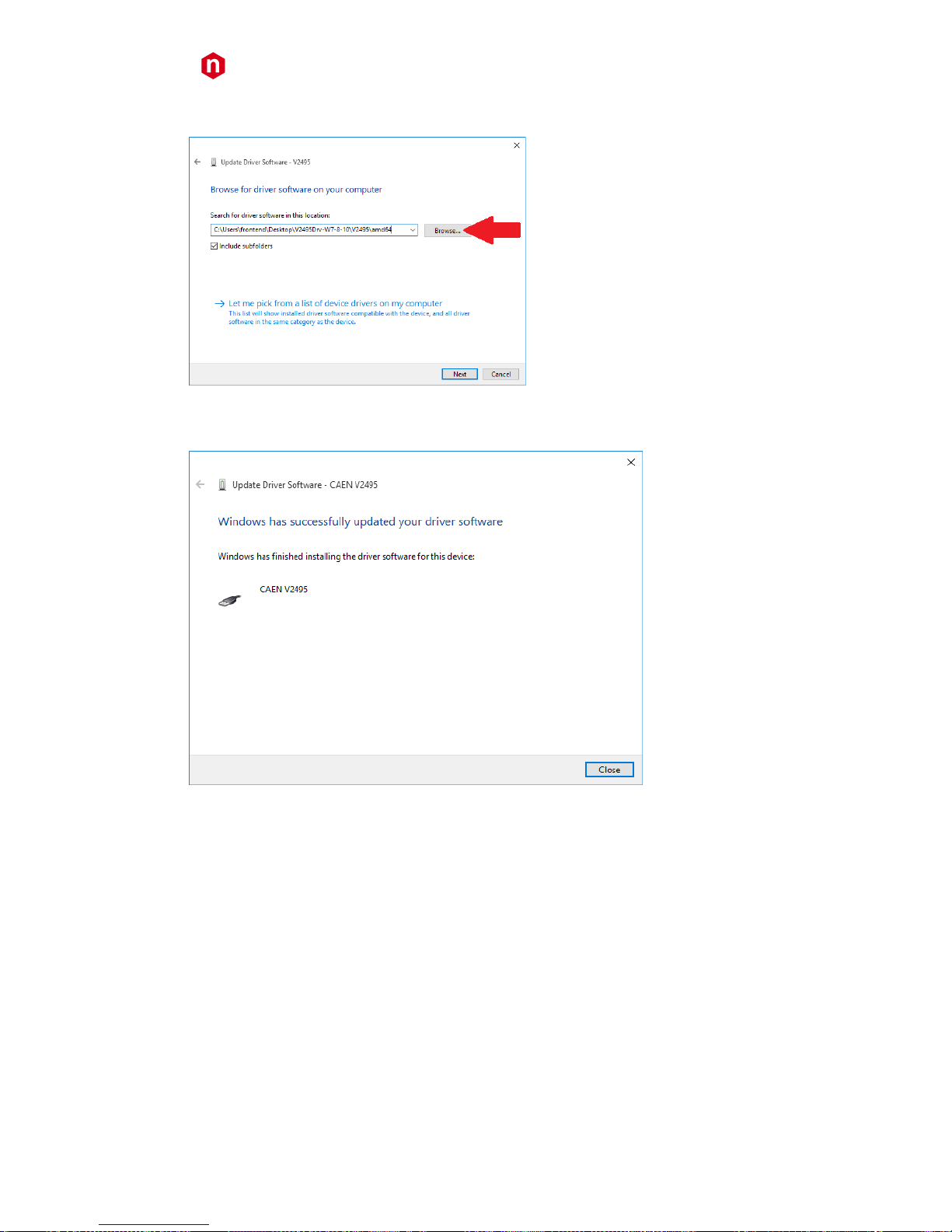
6. Use the [Browse] button to point to the driver folder in the destination path on the host PC.
Fig. 8.4: USB driver manual installation: Step3
7. Click the [Close] button at the end of the installation process.
Fig. 8.5: USB driver manual installation: Step4
Page 27
CAEN
Electronic Instrumentation
UM6508 – DT5495 User Manual rev. 0
27
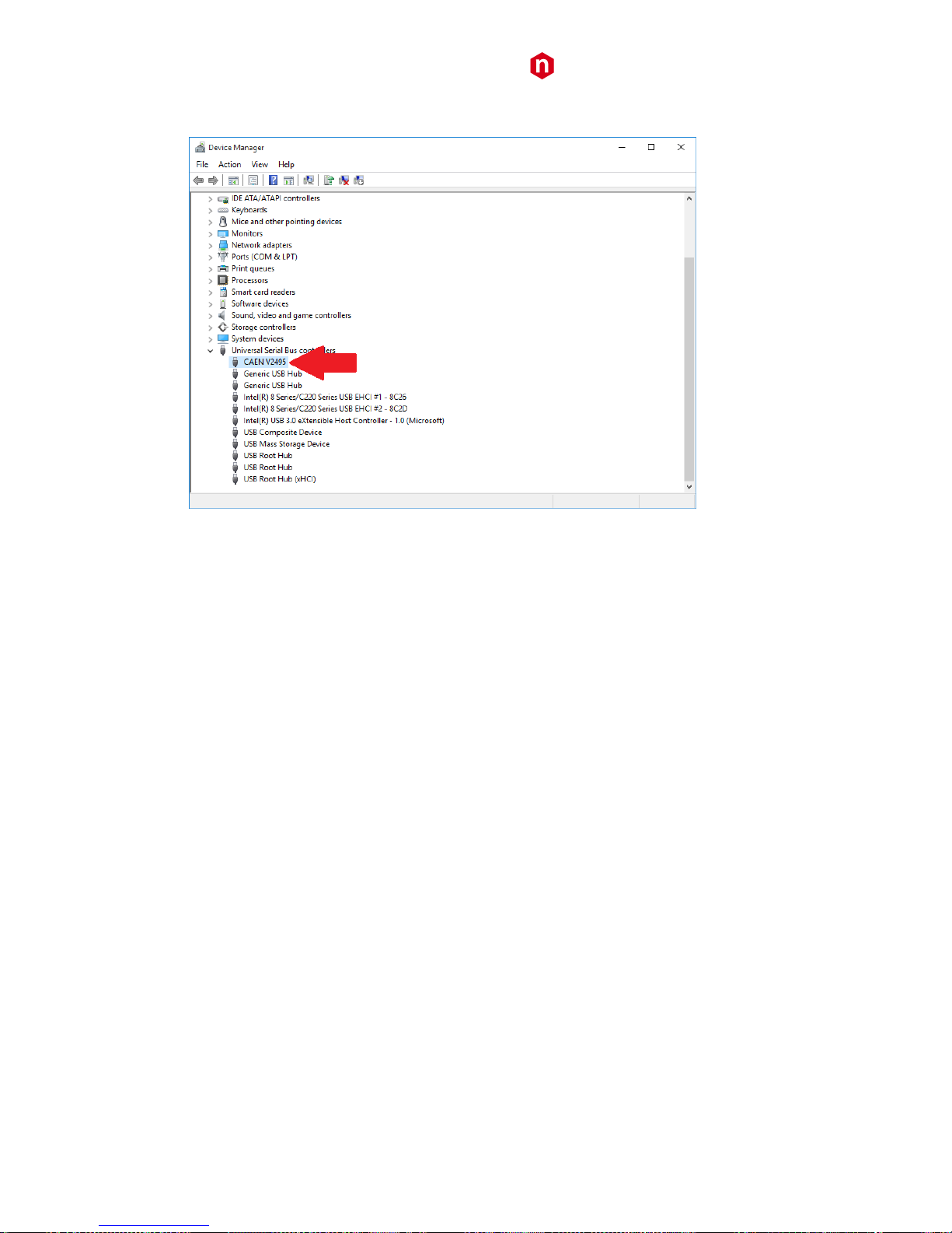
8. Check that the “CAEN V2495“ item appears in the Universal Serial Bus controllers list.
Fig. 8.6: USB driver manual installation: Step5
➢ Linux OS
DT5495 is fully supported by Linux kernels from kernel version 3.13 on. This means that such kernel versions should be
able to recognize the hardware automatically, without requiring the user to install any driver.
Note: the in-Linux drivers don’t automatically give to the user the rights to directly connect to the board. It is then
recommended to authenticate as root or to enable the low-level user rights before to try any communication by
software.
Page 28

CAEN
Electronic Instrumentation
UM6508 – DT5495 User Manual rev. 0
28
8.2 Ethernet Configuration
1. Connect the Ethernet cable between Hexagon and the PC.
2. Configure the Ethernet network of your PC in the following steps.
a. Open the path: Control Panel - Network and Internet - Network and Sharing Center (Fig. 8.13).
Fig. 8.7: The Network and Sharing Center window
b. Click on ”Change adapter settings”.
c. Right click on the Ethernet icon and select ”Properties” from the slide menu (Fig. 8.8).
Fig. 8.8: Properties window of the Ethernet network
Page 29

CAEN
Electronic Instrumentation
UM6508 – DT5495 User Manual rev. 0
29
d. Click on ”Internet Protocol Version (TPC/IPv4)”, and select ”Properties” (Fig. 8.9).
Fig. 8.9: Ethernet Properties window”
e. Copy the configuration as in Fig. 8.10 on the ”Internet Protocol Version (TPC/IPv4) Properties” window.
Fig. 8.10: Properties window of the ”Internet Protocol Version (TPC/IPv4)”
Note: Considering the factory default IP address of Hexagon is 192.168.0.90, use for the Network settings of the PC the
same first three IP Address numbers of the Hexagon IP, while make sure to set the fourth decimal number to a value
different from the Hexagon one to avoid IP conflicts over the net.
It is finally possible to connect to Hexagon by the Web Interface described in the next section (Sec. Web Interface).
Page 30
CAEN
Electronic Instrumentation
UM6508 – DT5495 User Manual rev. 0
30
8.3 Web Interface
Note: Check that the DT5495 is powered on, the Ethernet cable is connected, and the Network is set according to Sect.
Ethernet Configuration.
Open the web browser and type the DT5495 IP Address as web address. In the default case, the IP Address is
192.168.0.90:
http://192.168.0.90
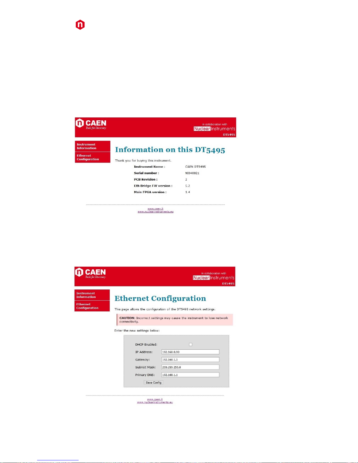
The Web Interface will enter the “Instrument Information” page (Fig. 8.11).
Fig. 8.11: Instrument Information page of the DT5495 Web Interface
Information includes the name, the serial number, the PCB revision, the revision of the Ethernet Bridge and the Main
FPGA firmware version.
Selecting “Ethernet Configuration”, the Web Interface shows the page where the ethernet settings can be changed by
the user.
Fig. 8.12: Instrument Information page of the DT5495 Web Interface
Press the “Save Config” button after modifications and remind to power cycle the board to make the new settings
effective.
Page 31
CAEN
Electronic Instrumentation
UM6508 – DT5495 User Manual rev. 0
31
8.4 Software Tools
CAENUpgrader
CAENUpgrader is a software tool available for Windows® and Linux® OS, 32 and 64-bit. The documentation [RD1] and
installation packages can be downloaded on CAEN web site at the CAENUpgrader web page (login required).
CAENUpgrader allows to perform the following operations on the DT5495 board:
• Upgrade the MFPGA firmware
• Load the User firmware on the UFPGA
• Verify the Main and User FPGA firmware
• Read the release number of the MFPGA firmware
• Store and get the Product Unlock Code in case of paid firmware
• Get the Board Info file (useful in case of support requests)
CAENUpgrader can operate with Windows and Linux, 32 and 64-bit OSs
The software installation package can be downloaded from CAEN web site (login required) at the CAENUpgrader web
page.
For any installation and functions which are not described in this manual, please refer to CAENUpgrader
documentation.
➢ Get the DT5495 Main FPGA Firmware Release
The following instructions allow to read the release number of the MFPGA firmware:
1. Select the “Get Firmware Release” option in the Board tab.
2. Select the “V2495” item in the Board Model combo box.
3. Set the connection parameters according to your communication link and hardware setup (all the parameters
are detailed in [RD1]).
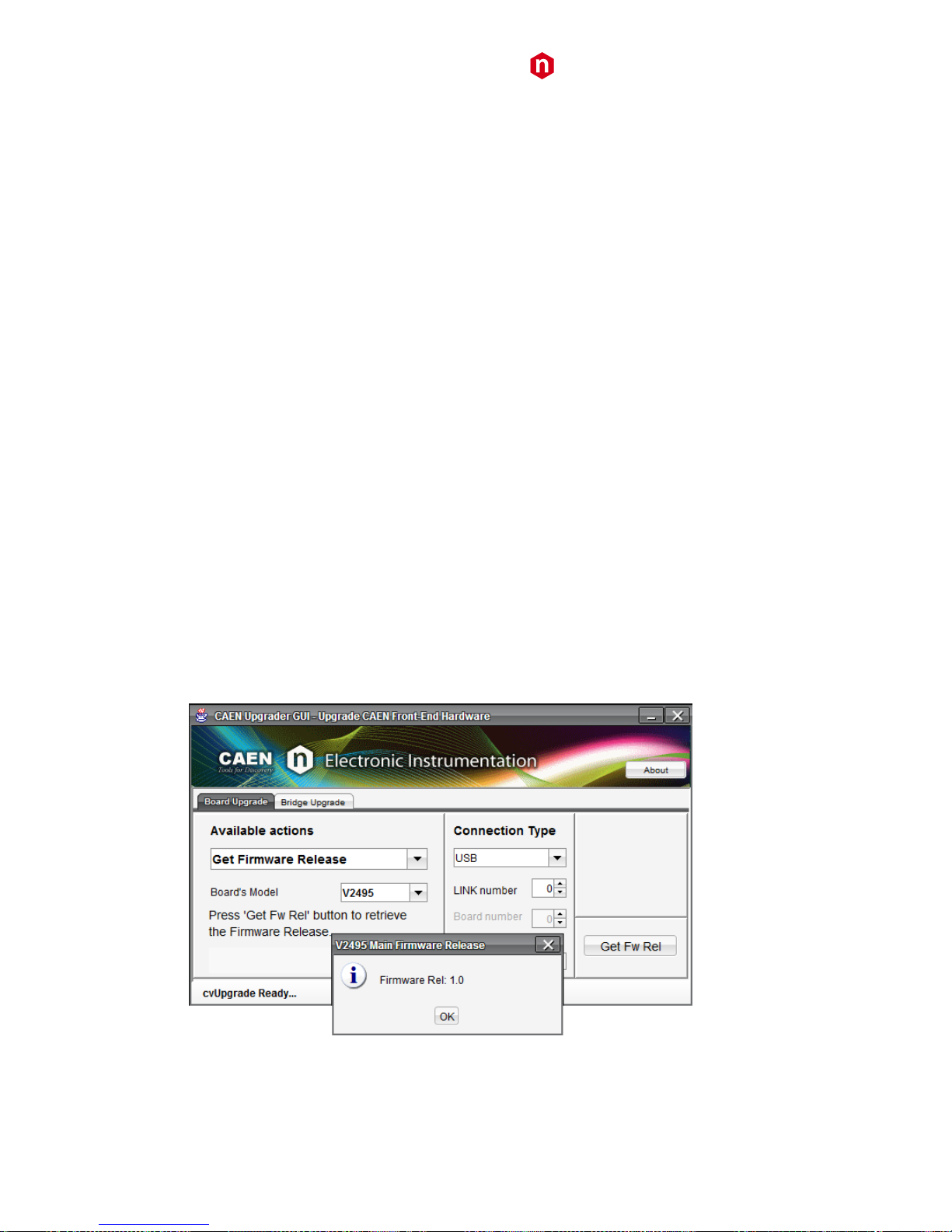
4. Press the Get FW Rel button. The software displays the release number in a message window (see Fig. 8.13).
Fig. 8.13: CAENUpgrader Get Firmware Release menu
Page 32

CAEN
Electronic Instrumentation
UM6508 – DT5495 User Manual rev. 0
32
➢ Upgrade the DT5495 Main FPGA Firmware
The MFPGA firmware can be downloaded from CAEN website at the DT5495 web page (login required):
The firmware file is available in Altera RPD format.
The following instructions allow to upgrade the MFPGA firmware:
1. Select the “Upgrade Firmware” option in the Board tab.
2. Select the “DT5495” item in the Board Model combo box.
3. Set the connection parameters according to your communication link and hardware setup (all the parameters
are detailed in [RD1]).
4. Select the MFPGA by checking the relevant checkbox.
5. Select the Main application firmware RPD file.
6. Press the Upgrade button. The outcome of the upgrade process is shown in a message window (see Fig. 8.14).
7. Power cycle the board to reconfigure the MFPGA with the firmware just updated on the flash. Please refer to
Sect. Power-on Configuration Sequence to check the outcome of the process.
Fig. 8.14: CAENUpgrader MFPGA Upgrade Firmware menu
Page 33

CAEN
Electronic Instrumentation
UM6508 – DT5495 User Manual rev. 0
33
➢ Upgrade the DT5495 User FPGA Firmware
The UFPGA demo firmware projects are available on CAEN website at the DT5495 web page (login required).
User demo firmware or custom user firmware can be recompiled and the generated RPD file can be uploaded into the
FLASH memory of the User FPGA.
The custom or the Demo RPD firmware file can be uploaded only on the application 1 page of
the USER FPGA FLASH of the DT5495!
The following instructions allow to upgrade the UFPGA firmware:
1. Select the “Upgrade Firmware” option in the Board tab.
2. Select the “V2495” item in the Board Model combo box.
3. Set the connection parameters according to your communication link and hardware setup (all the parameters
are detailed in [RD1]).
4. Select the UFPGA by checking the relevant checkbox.
5. Select Application 1 as the only supported target application image (see Fig. 8.15).
Fig. 8.15: CAENUpgrader UFPGA flash memory image menu
6. Select your User firmware or a CAEN Demo firmware RPD file.
7. Press the Upgrade button. The outcome of the upgrade process is shown in a message window (see Fig. 8.16).
At the end of the upgrade process, the CAEN Upgrader will force a reconfiguration of the UFPGA from the selected user
application image.
Fig. 8.16: CAENUpgrader UFPGA Upgrade Firmware menu
Page 34

CAEN
Electronic Instrumentation
UM6508 – DT5495 User Manual rev. 0
34
PLULib Library
CAEN PLULib library is a library of C functions developed to control V2495/VX2495 and DT5495 programmable logic
units through direct USB and Ethernet communication interfaces, but also through the VMEbus connection by using
CAEN Bridges (V2718 and V1718), if supported.
The library includes a simple demo application, which is not intended for the board readout, but rather to
automatically test the library functions. The user can then inspect the code as reference for his customized software
development based on the PLU library.
Fig. 8.17: CAEN PLULib Demo application prompt
CAEN PLULib library can operate on Windows® and Linux®, 32 and 64-bit. The documentation [RD3] and installation
packages can be downloaded on CAEN web site at the CAEN PLULib web page (login required).
Page 35

CAEN
Electronic Instrumentation
UM6508 – DT5495 User Manual rev. 0
35
9 Software Interface
The DT5495 board can be accessed via both Ethernet and USB interface. All registers are accessible from both
communication interfaces.
9.1 Address Map
The following table illustrates the DT5495 address map:
Address
Description
0x0000-0x0FFF
UFPGA data access
0x1000-0x7FFF
UFPGA register access
0x8000-0x80FF
reserved
0x8100-0x81FF
Configuration ROM
0x8200-0x83FF
Configuration and Status Registers
0x8400-0x84FF
Reserved
0x8500-0x86FF
MFPGA flash configuration
0x8700-0x88FF
UFPGA flash configuration
0x8900-0x8AFF
GDG flash configuration
0x8B00-x8BFF
Reserved
0x8C00-0x8FFF
Internal scratch RAM
0x9000-0xFFFF
reserved
Tab. 9.1: DT5495 register address map
User FPGA Data Access (0x0000-0x0FFF)
The UFPGA data access space is allocated specifically for the readout of data produced in the UFPGA logic which need
to exploit the maximum readout throughput available. This space can be accessed by using the available block transfer
mechanism over the Ethernet or USB communication interfaces.
Block data transfer allows to implement a faster readout. Block transfers requests over Ethernet or USB do not trigger
any transfer over the internal local bus between the MFPGA and UFPGA: a data prefetch mechanism, implemented in
the MFPGA, stores User data into a local data queue (prefetch data queue). Please, refer to the prefetch mechanism
description in Sect Local Bus Interface. Consequently, data from the UFPGA data access space are read from the
prefetch data queue in the MFPGA.
User FPGA Register Access (0x1000-0x7FFF)
UFPGA register address range is allocated for User register read/write.
A read or write transfer (single cycle) can be triggered on the local bus by performing a corresponding read transfer in
the 0x1000-0x7FFF address interval.
The local bus master in the MFPGA acts as a transparent bridge between the communication interface (ETH/USB) and
the local bus in this interval. A couple of examples are given to illustrate the transparent bridge behaviour.
Page 36

CAEN
Electronic Instrumentation
UM6508 – DT5495 User Manual rev. 0
36
Configuration ROM (0x8100-0x81FF)
The following registers contain module configuration information according to Tab. 9.2.
Only the 8 LSBs of each location of the Configuration ROM are significant.
Description
Address
Content
checksum
0x8100
An eight bit 2’s complement binary checksum. The
sum of the bytes starts from offset 0x8104 for the
number of bytes specified in the length field
(inclusive)
checksum_length2
0x8104
0x00
checksum_length1
0x8108
0x00
checksum_length0
0x810C
0x20
constant2
0x8110
0x84
constant1
0x8114
0x84
constant0
0x8118
0x01
c_code
0x811C
0x43
r_code
0x8120
0x52
oui2
0x8124
0x00
oui1
0x8128
0x40
oui0
0x812C
0xE6
version
0x8130
0x00
board2
0x8134
0x00
board1
0x8138
0x09
board0
0x813C
0xBF
revis3
0x8140
0x00
revis2
0x8144
0x00
revis1
0x8148
0x00
revis0
0x814C
PCB revision
sernum1
0x8180
Serial Number (MSB)
sernum0
0x8184
Serial Number (LSB)
Tab. 9.2: ROM Address Map of the DT5495
Note: The oui0/1 fields represent CAEN Manufacturer identifier (IEEE OUI), which is equal to 0x40E6.
Note: The board serial number can be read with two accesses: if the serial number on the module front panel is 1245
(hex 0x4DD), for instance, the Serial Number’s MSB (0x8180) will be 0x04, while the Serial Number’s LSB (0x8184) will
be 0xDD.
Configuration and Status Registers (0x8200-0x83FF)
Address
Register/Content
Read/Write
0x8200
MFPGA firmware revision
R
0x8204 ÷ 0x8214
reserved
0x8218
Software reset
W
0x8220
Scratch register
R/W
0x8224 ÷ 0x83FC
reserved
-
Tab. 9.3: CSR registers
Page 37
CAEN
Electronic Instrumentation
UM6508 – DT5495 User Manual rev. 0
37
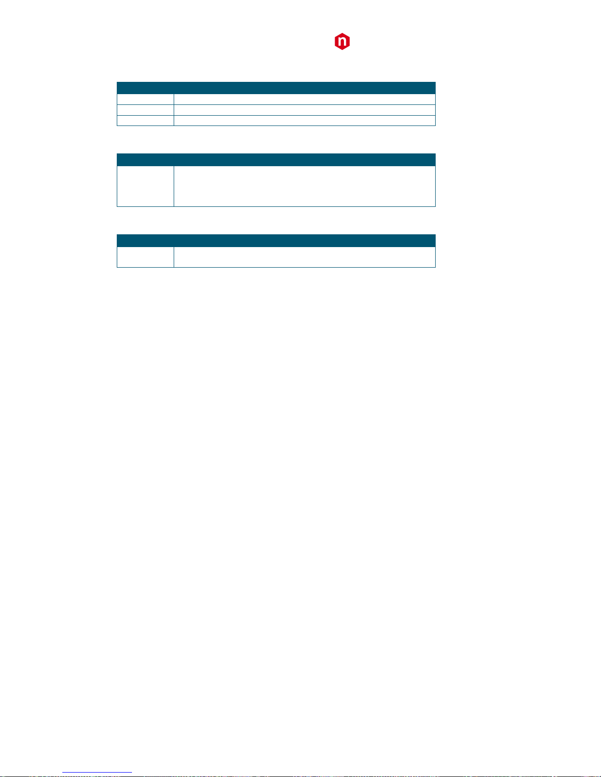
MFPGA Firmware Revision Register
Bit
Description
[31:16]
reserved
[15:8]
Major revision number
[7:0]
Minor revision number
Software Reset Register
Bit
Description
[31:0]
The value written into this register will determine the kind of software
reset:
1 = generate a local bus reset only (nLBRES local bus signal)
Others = reserved for future options
Scratch Register
Bit
Description
[31:0]
This register allows to perform 32-bit accesses for test purposes. Default
value is 0xAAAAAAAA
Flash Configuration (0x8500-0x8AFF)
This address range is reserved to flash remote programming.
Note: access to the FLASH is through the provided functions of the PLULib library (see Sect. Software Tools).
Internal Scratch SRAM(0x8C00-0x8FFF)
This area is available either for test access or for volatile data storage. Any address in this interval is implemented by an
internal RAM location.
Page 38

CAEN
Electronic Instrumentation
UM6508 – DT5495 User Manual rev. 0
38
10 Firmware Development
10.1 Introduction
The goal of this chapter is to let the user familiarize with the information and the tools needed to develop proprietary
firmware for the DT5495 board. A thorough description of the main firmware functionalities will be provided; the
features of essential components like the local bus interface and the gate and delay generator will also be discussed.
The four demos provided in the UFPGA flash memory will also be discussed: a step-by-step guide will be given to run
the examples. Their goal is to provide an extensive overview of the main functionalities of the DT5495 board and of its
mezzanine cards. The code of these demos, together with a template firmware, can be downloaded from the CAEN
website. When developing custom projects, it is recommended to start with the included template firmware, as it
includes the correct FPGA pinning and constraints. A short description of the user top-level I/O signals will also be
given.
The DT5495 board is the desktop format of an upgraded version of the V1495 board. The two boards have the same
I/O connectors and mezzanine card support. On the firmware development side, there are differences, mainly due to
the new Gate and Delay Generator and to the newly-introduced USB connection and Ethernet one. Please refer to
Sect. Porting V1495 to DT5495 for the details to port the V1495 projects on the DT5495 board.
Note: Due to the different I/O pin mapping and FPGA devices, the FPGA bit-streams and the projects previously
developed for the V1495 board are not compatible with the DT5495 board.
Page 39

CAEN
Electronic Instrumentation
UM6508 – DT5495 User Manual rev. 0
39
10.2 User FPGA I/O ports
This section illustrates the I/O ports of the UFPGA. Port names are the same of the VHDL entity top-level ports used in
the template and demo firmware.
➢ Clock: The user FPGA receives the board system clock
SIGNAL NAME
WIDTH
TYPE
DESCRIPTION
CLK
1
Input
50 MHz system clock
Tab. 10.1: Clock ports description table
➢ Mainboard Robinson Nugent connector ports: the ports A and B are input only. They feature 32 input channels that
reach the UFPGA as 32 single-ended LVTTL lines (3.3 V).
SIGNAL NAME
WIDTH
TYPE
DESCRIPTION
A
32
Input
A-port values
B
32
Input
B-port values
C
32
Output
C-port value
Tab. 10.2: Mainboard Robinson-Nugent connector description table
➢ LEMO ports: each of the LEMOs on the front panel can be used as input or output. The signals used are the
following:
SIGNAL NAME
WIDTH
TYPE
DESCRIPTION
GIN
2
Input
Input values for G0, G1
GOUT
2
Output
Output values for G0, G1
SELG
Output
NIM/TTL selector
0 = NIM
1 = TTL
nOEG
Output
Output enable (active low) (0=output, 1=input)
Tab. 10.3: LEMO G ports description table
➢ Expansion I/O ports: for each mezzanine, Tab. 10.4 shows the supported signals (X = D, E, F).
SIGNAL NAME
WIDTH
TYPE
DESCRIPTION
IDx 3 Input
Card ID
“000” = A395A
“001” = A395B
“010” = A395C
“011” = A395D
“100” = A395E
“111” = No mezzanine present
SELx
1
Output
NIM/TTL selector
0 = NIM
1 = TTL
nOEx
1
Output
Output enable (active low)
0 = output
1 = input
X
32
Input/Output
Data bus to/from the mezzanines
Tab. 10.4: Expansion I/O ports description table
Please note that:
• The SELx and nOEx signals are meaningful only for the A395D mezzanine card. When this mezzanine is not used,
these signals can be left undriven.
• Mezzanines with 32 I/O signals have a one-to-one correspondence between physical signals and I/O pins (i.e.
X[i] corresponds to the i-th channel of the mezzanine).
Page 40

CAEN
Electronic Instrumentation
UM6508 – DT5495 User Manual rev. 0
40
In case the A395D mezzanine is used, the mapping between the external channels and the X bus is shown in
Tab. 10.5. A schematic view of the A395D board is shown in Fig. 10.1.
CHANNEL
INPUT SIGNALS
OUTPUT SIGNALS
0
X[2]
X[0] 1 X[18]
X[16] 2 X[3]
X[1] 3 X[19]
X[17] 4 X[14]
X[12] 5 X[30]
X[28] 6 X[15]
X[13] 7 X[31]
X[29]
Tab. 10.5: A395D mapping
Fig. 10.1: CAENComm Demo Java and LabVIEW graphical interface
For example:
• A395D channel 0 can be driven with signal X[0] and its status can be read from X[2].
• A395D channel 1 can be driven with signal X[16] and its status can be read from X[18].
➢ User LEDs: Refer to the eight User LEDs on the front panel (see Chap. 4).
SIGNAL NAME
WIDTH
TYPE
DESCRIPTION
LED
8
Output
LED drivers
Tab. 10.6: LED ports description table
In order to switch on one of the eight LEDs on the front panel, the corresponding signal (LED[7:0]) should be set to 1.
➢ Gate & Delay Generator interface ports: The GDG is connected to the UFPGA via the following signals:
SIGNAL NAME
WIDTH
TYPE
DESCRIPTION
GD_START
32
Output
GDG start signals
GD_DELAYED
32
Input
GDG output signals
SPI_MISO
1
Input
SPI MISO (Master Input Slave Output)
SPI_SCLK
1
Output
Serial clock
SPI_CS
1
Output
SPI Chip Select
SPI_MOSI
1
Output
SPI MOSI (Master Output Slave Input)
Tab. 10.7: Gate and Delay Generator ports description table
Page 41
CAEN
Electronic Instrumentation
UM6508 – DT5495 User Manual rev. 0
41
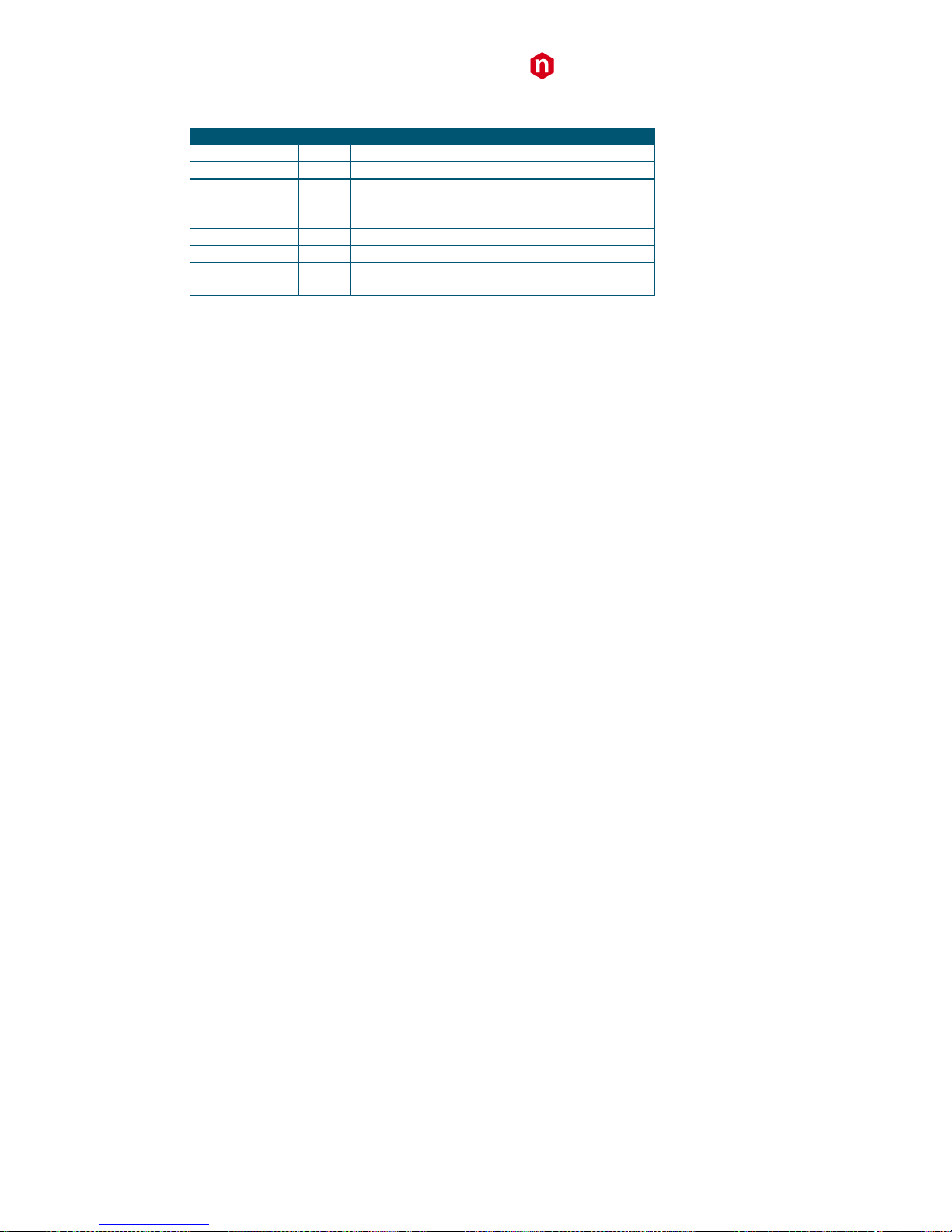
➢ Local Bus ports: The Local Bus signals are shown in Tab. 10.8.
SIGNAL NAME
WIDTH
TYPE
DESCRIPTION
nLBRES
1
Input
Bus reset (active low)
nBLAST
1
Input
Last cycle (active low)
WnR
1
Input
Write/Read cycle
0 = read
1 = write
nADS
1
Input
Address strobe (active low)
nREADY
1
Output
Slave ready/Prefetch request
LAD
32
Input/Ou
tput
Data/address bus
Tab. 10.8: Local Bus ports description table
Page 42

CAEN
Electronic Instrumentation
UM6508 – DT5495 User Manual rev. 0
42
10.3 Local Bus Interface
The Local Bus (LB) is the communication interface between the MFPGA and the UFPGA.
It is made of a Master (LBM), implemented inside the MFPGA, and of a Slave (LBS), implemented inside the UFPGA. The
communication protocol between the LBM and the LBS is based on the following signals. In what follows OUT(IN)
means that the signal goes from the LBM(LBS) to the LBS(LBM) and AL stands for active-low:
• nADS (OUT, AL): it is set by the LBM when a r/w operation is performed. The LBS samples the register address
from LAD when nADS is set.
• WnR (OUT): it notifies the LBS whether the access is in write- (WnR=1) or read- (WnR=0) mode. The value of
WnR is relevant only when nADS is set.
• nREADY (IN, AL): It is a dual-purpose signal. it is set by the LBS to notify the LBM that the LBS is ready for r/w
data transfer. It can also be used for the data prefetch mechanism (see next).
• nBLAST (OUT, AL): it signals the last cycle of a data transfer. It is set when either the LBS is not ready, or the
LBM, cannot accept data (e.g. because the FIFO used for data prefetch is full).
• LAD (IN/OUT): the 16-bit bus used to read/write both address and data.
LBM can generate two kind of transfers over the local bus:
• Single word (32-bit) read/write transfer
• Multi word prefetch transfer
Single word transfers are initiated by the LBM for register access. It it composed by a single clock address phase and
two 16-bit data phases. A data phase is completed if the LBS asserts nREADY low. The transfer ends on the second data
phase when the LBM asserts the nBLAST signal low.
Examples of the signal logic taken using AlteraTM Signal Tap are shown in Fig. 10.2 and Fig. 10.3. For a read and a write
access on the LBS.
Fig. 10.2: Local bus signals at a write access (x8BADF00D is written on register x1800)
Fig. 10.3: Local bus signal at a read access (x8BADF00D is read from register x1800)
Page 43

CAEN
Electronic Instrumentation
UM6508 – DT5495 User Manual rev. 0
43
A data prefetch mechanism, implemented in the MFPGA, stores User data into a MFPGA local data queue (prefetch
data queue). The MFPGA prefetch queue data is available for readout over the Ethernet or USB interface (see Sect.
Address Map).
The prefetch mechanism is illustrated by Fig. 10.4.
nADS
LAD
WnR
nBLAST
nREADY
MAIN
FPGA
USER
FPGA
LOCAL BUS
LOCAL
BUS
MASTER
LOCAL
BUS
SLAVE
PREFETCH
DATA
QUEUE
USER
DATA
QUEUE
Fig. 10.4: Prefetch mechanism
Prefetch read cycles are initiated by the UFPGA logic: nREADY local bus signal must be used by the User logic to request
a new data prefetch cycle by the local bus master (MFPGA): The request is active when the nREADY is low. The local
bus master should have an internal prefetch queue (FIFO component). If a user request is pending and the local bus
master has available space into the prefetch queue, it will start an internal block transfer from local bus address
0x0000 (fixed). The User logic is required to respond only to address 0x0000: data from its data queue are made
available to the DT5495 local bus. If a new register access is requested to the local bus master while a prefetch cycle is
ongoing, the prefetch cycle will be interrupted by asserting the nBLAST signal and the register access will be served
with priority. At the end of a register access, the user logic can keep the nREADY signal active to request a new prefetch
cycle to the LBM, which will fetch new data in its queue.
Please refer to the lb_int.vhd source code in the User demo firmware projects.: it is a Local Bus slave implementation
provided by CAEN as a reference.
The lb_int.vhd found in the Pattern Recorder demo firmware (see Sect. Pattern Recorder Demo Description) is a
demonstration of user logic implementation of the data prefetch mechanism.
Page 44
CAEN
Electronic Instrumentation
UM6508 – DT5495 User Manual rev. 0
44
10.4 Gate and Delay Controller
General Description
The GDG can be used by the user logic to gate and delay up to 32 digital signals. The delay and gate values can be set
using a dedicated serial bus (SPI bus). The signals are sent to the GDG, where they are gated and delayed according to
the user settings and then returned to the UFPGA. The width of the delayed signal only depends on the gate value set
and is not related to the width of the incoming signal.
The gate and delay values are 16-bit wide and their sum cannot exceed 65535 (0xFFFF). They are both generated by
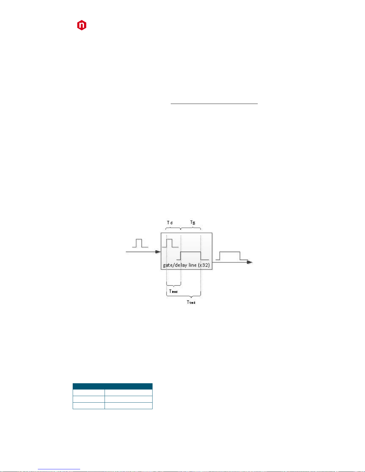
using an internal clock, which computes the number of clock cycles between the incoming signal and the leading and
trailing edge of the gate signal. Referring to Fig. 10.5, the times of occurrence of the leading (T
lead
) and trailing (T
trail
)
can be obtained using the following formulas, where Ng(Nd) is the gate(delay) value set by register and T0, T1 are the
time values reported in Tab. 10.9:
T
lead
= 0 if Nd=0
T0+T1(Nd-1) if Nd>0
T
trail
= 0 if Nd=Ng=0
T0+T1(Nd+Ng-1) if (Nd+Ng)≥1
The relationship between T
lead
, T
trail
and the delay and gate duration is:
T
delay=Tlead
T
gate=Ttrail-Tlead
Fig. 10.5: Gate and Delay parameters representation
T1 represents the minimum increment of either the gate or the delay value. The presence of T0 is due to a slightly
longer duration of the minimum delay time increment (or gate increment, if the Ng=0) with respect to the standard T1
increment. It should be noted that both T1 and T0 can vary from channel to channel, with an expected variation interval
of ±10% for both. Please also consider that, when setting Nd=0, the observed delay of the outgoing signal with respect
to the incoming one is due to the paths on the PCB and inside the FPGAs, which are delay channel-dependent.
Example 1: If the delay value is set to 0x0 and the gate value is set to 0x5, the gate will last 12.2+10.7*4=55 ns.
Example 2: If the delay value is set to 0x8 (typ. 12+7*10.7=86.9 ns), the maximum possible gate value is 0xFFF8 (typ.
65527*10.7 ≈ 701 µs).
Example 3: If the delay value is set to 0xFFF8 (≈ 701 µs), the ma maximum possible gate value is 0x8 (typ. 86.9 ns).
PARAMETER
VALUE
T0
12 ns (typ.) ± 10%
T1
10.7 ns (typ.) ± 10%
T
max
T0 + T1 (216-1)
Tab. 10.9: Main parameters of the Gate and Delay Generator
Page 45

CAEN
Electronic Instrumentation
UM6508 – DT5495 User Manual rev. 0
45
The UFPGA can set the relevant configuration registers and read data from the generator through the SPI protocol.
CAEN does not provide a detailed description of the communication protocol over the SPI bus for GDG configuration. A
VHDL component is provided in the gd_control.vhd source code (GD_CONTROL), included in all the user demo
firmware.
GD_CONTROL implements the following registers that can be accessed from the local bus. The LB_INT component
reserves addresses starting from 0x7F00 to GD_CONTROL access. LB_INT and GD_CONTROL are connected by a
dedicated interface for register write and read.
A set of LB registers are used to configure the GDG, as described in Tab. 10.10:
ADDRESS
REGISTER/CONTENT
ACCESS MODE
Read/Write
0x7F00
0x7F04
0x7F08
0x7F0C
0x7F10
Data Write
Command register
Control register
Data read
Status register
A24/A32
A24/A32
A24/A32
A24/A32
A24/A32
D16/D32
D16/D32
D16/D32
D16/D32
D16/D32
R
R
R
R
R
Tab. 10.10: Local Bus registers description for the Gate and Delay Generator configuration
Register Description
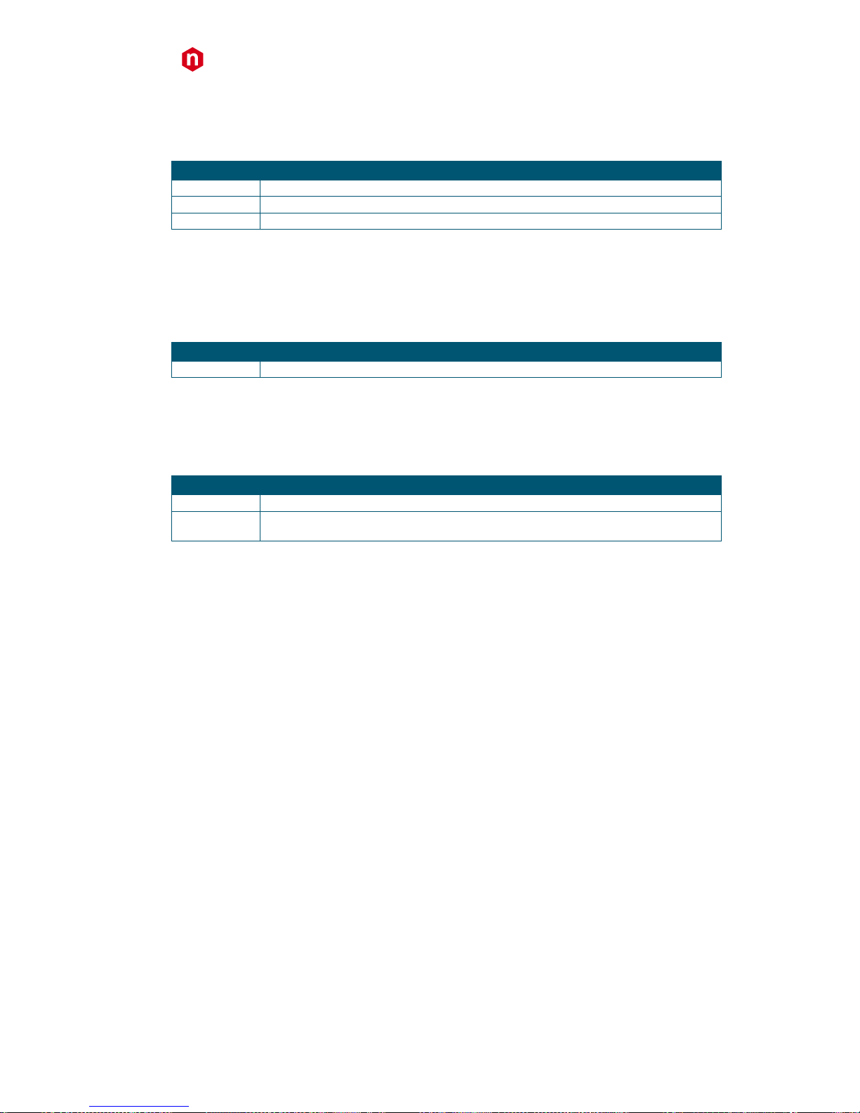
➢ DATA WRITE: the datum (gate or delay) must be written here before it is transmitted through SPI to the GDG.
Address: 0x7F00.
Mode: Read only.
Bit
Description
[31:0]
Gate or delay datum to transmit to the GDG
➢ COMMAND register: it is where the action to be performed is set. The action depends on the value of the 2 LSBs of
the Control register (read or write mode): one of these bits should be asserted to execute the related action. The
channel interested by the action is set through the 6 LSBs of the register (relevant when [15:0] = 0x100 in write
mode and [15:0] = 0x2000, 0x3000 in read mode).
Address: 0x7F04
Mode: Read only
Write Mode
Bit
Description
[31:16]
reserved
[15:0]
0x2000 = the internal gate value is modified with the content of the data write register (but
not sent to the DFPGA)
0x3000 = the internal delay value is modified with the content of the data write register (but
not sent to the DFPGA)
0x0100(+channel) = the gate AND delay values of the selected channel are modified with the
internal values, sent to the DFPGA by the UFPGA through SPI
0x0300 = the delay of all channels is reset
0x0400 = the delay of all channels is calibrated
0x0500 = the internal gate and delay values are broadcast to all 32 channels
Read Mode
Bit
Description
[31:16]
reserved
[15:0]
0x2000(+channel) = the gate value of the specified channel is read through SPI
0x3000(+channel) = the delay value of the specified channel is read through SPI
Page 46
CAEN
Electronic Instrumentation
UM6508 – DT5495 User Manual rev. 0
46
➢ CONTROL register: bit[0] sets a write or read action.
Address: 0x7F08.
Mode: Read only.
Bit
Description
[31:2]
reserved
[1]
1 = a read action is performed
[0]
1 = a write action is performed
➢ DATA READ: it is where the datum (gate or delay) can be read after an SPI read access to the GDG has been
performed (see the Read Mode of the COMMAND register).
Address: 0x7F0C.
Mode: Read only.
Bit
Description
[31:0]
Gate or delay datum resulting from READ MODE access to GDG
➢ STATUS register
Address: 0x7F10.
Mode: Read only.
Bit
Description
[31:1]
reserved
[0]
Gate and delay ready signal (when 0, the Gate and Delay controller is busy. A new command
to the Gate and Delay controller should not be issued before this bit sets back to 1)
Example Procedures
• MODIFY THE GATE OR THE DELAY VALUE OF A CHANNEL
The gate or the delay of a signal from the UFPGA can be modified by following this procedure (the registers quoted are
accessible via VME):
- Set a delay (gate) value in the DATA WRITE register
- Set the COMMAND register to 0x2000 (0x3000) to modify the delay (gate) internal value
- Set the control register to 0x1/0x0
- Set the COMMAND register to 0x100 + CHANNEL (6 bits) to write the gate and delay values on the FPGA
through the SPI bus, for the channel specified by the six LSBs. Note that the gate and delay values are
written in the same action
- Set the CONTROL register to 0x1/0x0
• READ THE GATE OR THE DELAY VALUE OF A CHANNEL
- Set the COMMAND register to 0x2000 (0x3000) + CHANNEL (6 bits) to read the delay (gate) value of a
specific channel
- Set the CONTROL register to 0x2/0x0
- Read the required value in the DATA READ register
• BROADCAST A GATE OR DELAY VALUE OF A CHANNEL
- Set the desired values of the delay and gate values (see the first example, first two steps)
- Set the COMMAND register to 0x500
- Set the CONTROL register to 0x1/0x0
Note that in the case of a broadcast command the delay and gate values are serialized to the GDG at the same time.
The bits related to the channel index (six LSBs of the CONTROL register) are irrelevant in this case.
Page 47

CAEN
Electronic Instrumentation
UM6508 – DT5495 User Manual rev. 0
47
10.5 Porting V1495 to DT5495
Firmware designs targeted to the V1495 User FPGA can be ported to DT5495 by keeping in mind the following
differences between the two modules:
- The DT5495 FPGA device is different (Cyclone V versus Cyclone I) and with larger logic resources. While there will
be no resource constrains, the FPGA configuration scheme and output binary files are different for the two
boards.
- A design that used on-board delay lines with V1495 must be redesigned to consider the new features and
characteristics of the DT5495 GDG.
- The address map of the V1495 VME FPGA and DT5495 MAIN FPGA have some differences to consider:
o Registers in V1495 are mapped at 16-bit aligned addresses, while DT5495 features a 32-bit aligned address
map. Register access should always be in 32-bit mode.
o Common registers with different address:
• 0x800C in V1495
• 0x8200 in DT495
- The local bus map is the same for V1495 and DT5495. Block transfers are allowed only in the 0x0000-0x0FFF
address interval. The same user data prefetch mechanism is implemented. Local bus register accesses are mapped
to the same 0x1000-0x7FFF address interval.
Note: The DT5495 does not require the 0x100C local bus address to be reserved for user firmware revision register
with special constraints due to the firmware licensing mechanism. In DT5495, all user registers can be implemented in
the allowed address range without any constraints of functionality or content
- The flash access register map and protocol are different between the two boards: the specific setting and tools
must be used for each module.
Page 48

CAEN
Electronic Instrumentation
UM6508 – DT5495 User Manual rev. 0
48
11 Demo Firmware
11.1 Introduction
This chapter describes a set of UFPGA demos that CAEN provides as demonstration of the DT5495 functionalities and
as a guide for developing customized user application firmware.
The wanted demo can be stored only on the application 1 page of the UFPGA FLASH memory.
To run a firmware “as it is”, it is required to use the functions of the CAEN PLULib library to access the proper registers
(refer to Sect. Software Tools). To modify demos and upload the new firmware on the FPGA, a basic knowledge of
VHDL language and Altera Quartus II software are required.
In what follows, the features of the four demos loaded in the UFPGA’s flash memory will be described.
By default, each demo lights front panel user LED with the following configurations:
Demo
Description
Demo1
LED 0 ON; others OFF
Demo2
LED 1 ON; others OFF
Demo3
LED 1 and LED 0 ON; others OFF
Demo4
LED 2 ON; others OFF
11.2 Demo Structure
All demo projects feature a common file structure:
• A configuration file (V2495_package.vhd), allowing to set the number of CONFIG and MONITOR registers, their
respective base address, the demo ID and the firmware revision. The CONFIG registers are mapped between
0x1000 and 0x17FC, while the MONITOR registers are mapped between 0x1800 and 0x1FFC.
• A gate and delay block (gd_control.vhd), acting as a controller for the GDG (the example in Sect. Gate and Delay
Demo Description specifically focuses on the configuration of GDG delays);
• The local bus slave (lb_int.vhd), allowing to read/write the registers needed in the demo operations;
• The SPI master (spi_master.vhd) and interface (spi_interface.vhd), allowing the communication to/from the
GDG to be serialized;
• A demo-specific part, containing core demonstration logic.
11.3 Demo Setup
To run the demo firmware just stored in the application 1 page of the UFPGA FLASH memory, the following instructions
should be followed:
• Connect to the DT5495 board to read/write registers
• Set the required configuration through the control register(s).
Page 49

CAEN
Electronic Instrumentation
UM6508 – DT5495 User Manual rev. 0
49
11.4 Gate Pattern Demo Description
Introduction
In this example, a logic combination of the input port signals A and B is sent to the C connector (32 lines). The user can
choose the output among 10 available options by setting the 4 LSBs of the control register (see the register list). Apart
from the value of A, B, A AND B and A OR B, the aforementioned signals in “capture” mode (a bit is set whenever a
signal shows up) can be selected.
Register Map
In this example, 9 registers are used, 5 of which (MONITOR registers) can only be read and 4 (CONTROL registers) can
be both read and written. All registers are 32 bit wide and can be accessed in single access mode.
ADDRESS
REGISTER/CONTENT
ACCESS MODE
Read/Write
0x1000
0x1004
0x1008
0x100C
0x1010
0x1800
0x1804
0x1808
0x180C
Firmware version
Value of port A (input)
Value of port B (input)
Value of port C (output)
Status register
Mask of input port A
Mask of input port B
Control register
User Value of port C
A24/A32
A24/A32
A24/A32
A24/A32
A24/A32
A24/A32
A24/A32
A24/A32
A24/A32
D16/D32
D16/D32
D16/D32
D16/D32
D16/D32
D16/D32
D16/D32
D16/D32
D16/D32
R
R
R
R
R
R/W
R/W
R/W
R/W
Register Description
➢ FIRMWARE REVISION register: Contains the firmware revision number.
Address: 0x1000.
Mode: Read only.
Bit
Description
[31:0]
Firmware revision progressive number
➢ A-PORT VALUE register: Contains the 32 input bits of port A.
Address: 0x1004.
Mode: Read only.
Bit
Description
[31:0]
Input value of Port A
➢ B-PORT VALUE register: Contains the 32 input bits of port B.
Address: 0x1008.
Mode: Read only.
Bit
Description
[31:0]
Input value of Port B
➢ C-PORT VALUE register: Contains the 32 output bits of port C (selectable by the user in this demo).
Address: 0x100C.
Mode: Read only.
Bit
Description
[31:0]
Output value of port C
Page 50

CAEN
Electronic Instrumentation
UM6508 – DT5495 User Manual rev. 0
50
➢ STATUS register: Contains status information.
Address: 0x1010.
Mode: Read only.
Bit
Description
[31:5]
reserved
[4]
Register clear signal
[3]
Register gate signal
[2]
External clear signal
[1]
External gate signal
[0]
Data ready
➢ A-PORT MASK register: Masks the channels of port A.
Address: 0x1800.
Mode: Read and Write.
Bit
Description
[31:0]
The n-th bit set to 1 means that the corresponding channel of port A is masked
➢ B-PORT MASK register: Masks the channels of port B.
Address: 0x1804.
Mode: Read and Write.
Bit
Description
[31:0]
The n-th bit set to 1 means that the corresponding channel of port B is masked
➢ CONTROL register: Allows to set the demo configuration.
Address: 0x1808.
Mode: Read and Write.
Bit
Description
[31:9]
reserved
[8]
Allows to select the signal type on ports G0, G1: 0 = NIM level, 1 = TTL level
[7:6]
Reserved
[5]
The gate of input port C ends when this bit is set
[4]
The gate of input port C starts when this bit is set
[3:0]
0x0 = the port A (possibly masked) is sent to C when a gate signal is active.
0x1 = the port B (possibly masked) is sent to C when a gate signal is active.
0x2 = the AND of A and B (possibly masked) is sent t to C when a gate signal is active.
0x3 = the OR of A and B (possibly masked) is sent t to C when a gate signal is active.
0x4 = the port A (possibly masked) is captured and sent to C when a gate signal is active
0x5 = the port B (possibly masked) is captured and sent to C when a gate signal is active
0x6 = the AND of ports A and B (possibly masked) is captured and sent to C when a gate
signal is active
0x7 = the OR of ports A and B (possibly masked) is captured and sent to C when a gate
signal is active
0x8 = a clock counter (@ 50 MHz) is sent to C
0x9/0xF = the value of a register is sent to C
Page 51

CAEN
Electronic Instrumentation
UM6508 – DT5495 User Manual rev. 0
51
➢ C-PORT USER VALUE register: Allows to set the C port value when Control register bits[3:0] are set to 0x9/0xF.
Address: 0x180C.
Mode: Read and Write.
Bit
Description
[31:0]
User value of Port C
Page 52

CAEN
Electronic Instrumentation
UM6508 – DT5495 User Manual rev. 0
52
11.5 Pattern Recorder Demo Description
Introduction
In this demo, a digital pattern recorder is implemented. When a start signal is received, the digital input specified
through the control register is sampled at a user-configurable sampling rate, and a user-configurable number of
samples are collected in a FIFO. Once all samples have been stored, they can be readout through read accesses.
Register Map
In this example, 9 registers are used, 5 of which (MONITOR registers) can be only read and 4 (CONTROL registers) can
be both read and written.
The sampling clock can be either internal (100 MHz, generated from the 50 MHz input clock through a PLL) or external,
through the G0 connector: in this case a signal compatible with one of the supported levels (NIM or TTL) should be
provided.
All registers are 32 bit wide and can be accessed in single access mode.
ADDRESS
REGISTER/CONTENT
ACCESS MODE
Read/Write
0x0000
0x1000
0x1004
0x1008
0x100C
0x1800
0x1804
0x1808
0x180C
FIFO content readout
Firmware version
Value of port A (input)
Value of port B (input)
Value of port C (output)
Mask of input port A
Mask of input port B
Control register
User Value of port C
A24/A32
A24/A32
A24/A32
A24/A32
A24/A32
A24/A32
A24/A32
A24/A32
A24/A32
D16/D32
D16/D32
D16/D32
D16/D32
D16/D32
D16/D32
D16/D32
D16/D32
D16/D32
R
R
R
R
R
R/W
R/W
R/W
R/W
Register Description
➢ FIRMWARE REVISION register: Contains the firmware revision number
Address: 0x1000.
Mode: Read only.
Bit
Description
[31:0]
Firmware revision progressive number
➢ A PORT VALUE: the 32 input bits of port A
Address: 0x1004.
Mode: Read only.
Bit
Description
[31:0]
Input on port A
➢ B PORT VALUE: the 32 input bits of port B
Address: 0x1008.
Mode: Read only.
Bit
Description
[31:0]
Input on port B
Page 53

CAEN
Electronic Instrumentation
UM6508 – DT5495 User Manual rev. 0
53
➢ C PORT VALUE: the 32 output bits of port C (selectable by the user in this demo)
Address: 0x100C.
Mode: Read only.
Bit
Description
[31:0]
Output to port C
➢ A-PORT MASK register: Masks the channels of port A.
Address: 0x1800.
Mode: Read and Write.
Bit
Description
[31:0]
The n-th bit set to 1 means that the corresponding channel of port A is masked
➢ B-PORT MASK register: Masks the channels of port B.
Address: 0x1804.
Mode: Read and Write.
Bit
Description
[31:0]
The n-th bit set to 1 means that the corresponding channel of port B is masked
➢ CONTROL register: allows to set the demo configuration.
Address: 0x1808.
Mode: Read and Write.
Bit
Description
[31:20]
Number of stored samples in the FIFO
[19:16]
Downsampling factor (frequency divider)
[15:10]
reserved
[9]
Software acquisition start
[8]
Software acquisition stop
[7:6]
reserved
[5:4]
Output selection (port C)
00 = Port A
01 = Port B
10 = clock counter
11 = user output (register 0x180C)
[3:2]
reserved
[1]
The selected clock source
0 = internal clock source
1 = external clock source (G0 port)
[0]
I/O port level
0 = NIM level
1 = TTL level
➢ C PORT VALUE register: allows to set an arbitrary value to port C.
Address: 0x180C.
Mode: Read and Write.
Bit
Description
[31:0]
User output value for port C
Page 54

CAEN
Electronic Instrumentation
UM6508 – DT5495 User Manual rev. 0
54
11.6 DAC Demo Description
Introduction
In this demo, the use of a A395E mezzanine card to configure a DCC output value on its 8 output channels will be
explained. The DAC registers are 16 bits wide, and the dynamic range of the output voltage is +/- 5 V (refer to Tab. 5.6
for detailed specifications).
Register Map
In this example, 4 registers are used, 2 of which (MONITOR registers) can only be read and 2 (CONTROL registers) can
be both read and written. All registers are 32-bit wide and can be accessed in single access mode.
ADDRESS
REGISTER/CONTENT
ACCESS MODE
Read/Write
0x1000
0x1004
0x1800
0x1804
Firmware Version
Mezzanine ID number
Control register
DAC register
A24/A32
A24/A32
A24/A32
A24/A32
D16/D32
D16/D32
D16/D32
D16/D32
R
R
R/W
R/W
Register Description
➢ FIRMWARE VERSION register: Stores the revision number of the firmware.
Address: 0x1000.
Mode: Read only.
Bit
Description
[31:0]
Revision Number
➢ MEZZANINE ID NUMBER register: Contains the Mezzanine ID values (see Tab. 10.4).
Address: 0x1004.
Mode: Read only.
Bit
Description
[31:12]
reserved
[11:8]
Mezzanine ID, port F
[7:4]
Mezzanine ID, port E
[3:0]
Mezzanine ID, port D
➢ CONTROL register
Address: 0x1800.
Mode: Read and Write.
Bit
Description
[31:29]
reserved
[28]
Activation of test mode (sawtooth signal on all channels)
[27:25]
Reserved
[24]
1 = the DAC value is written for the specified mezzanine and channel
0 = the DAC value is read for the specified mezzanine and channel (the result is put in
0x1804)
[23:22]
reserved
[21:20]
Selects the mezzanine for either a write or read access
“00” = F
“01” = E
“10” = D
[19:16]
The 3 LSBs [18:16] select the channel for either a write or read access. If a write access is
performed and [19] = 1 all channels are selected for writing; if a read access is performed
[19] is ignored
[15:0]
DAC value
Page 55

CAEN
Electronic Instrumentation
UM6508 – DT5495 User Manual rev. 0
55
➢ DAC register: Contains the DAC value of the channel specified by bits[21:16] of the register 0x1800.
Address: 0x1804.
Mode: Read and Write.
Bit
Description
[31:0]
DAC value
Please, note that the DAC value obtained from register 0x1804 is not read from the chip, but it is the last set value for
that specific channel.
Page 56

CAEN
Electronic Instrumentation
UM6508 – DT5495 User Manual rev. 0
56
11.7 Gate and Delay Demo Description
Introduction
In this demo the functionalities and use of the Gate and Delay Generator will be shown. The signal to be delayed can be
selected between an internally-generated clock of configurable frequency (submultiples of 50 MHz) and the input from
the G0 connector (please refer to Sect. Gate and Delay Controller for the G0 and G1 port configuration required in this
case). An output signal of configurable width and delay with respect to the input signal’s leading edge will be available
on G1.
Register Map
In this example, 3 registers are used, 1 of which (MONITOR register) can be only read and 2 (CONTROL registers) can be
both read and written. All registers are 32-bit wide and can be accessed in single access mode.
ADDRESS
REGISTER/CONTENT
ACCESS MODE
Read/Write
0x1000
0x1800
0x1804
Firmware Version
Control register
Clock frequency register
A24/A32
A24/A32
A24/A32
D16/D32
D16/D32
D16/D32
R
R/W
R/W
The registers of the Gate and Delay controller are used to configure the GDG parameters.
ADDRESS
REGISTER/CONTENT
ACCESS MODE
Read/Write
0x7F00
0x7F04
0x7F08
0x7F0C
0x7F10
Data write register
Command register
Control register
Data read register
Status register
A24/A32
A24/A32
A24/A32
A24/A32
A24/A32
D16/D32
D16/D32
D16/D32
D16/D32
D16/D32
R/W
R/W
R/W
R
R
Register Description
➢ FIRMWARE VERSION register: Stores the revision number of the firmware.
Address: 0x1000.
Mode: Read only.
Bit
Description
[31:0]
Revision Number
➢ CONTROL register:
Address: 0x1800.
Mode: Read and Write.
Bit
Description
[8:4]
The DFPGA channel used to delay the input signal
[1]
Input signal selection:
0 = clock signal (frequency set by bits [8:4]
1 = G0 input
[0]
I/O port level selection:
0 = NIM level
1 = TTL level
WARNING: When the G0 connector is used as an input, the user should follow the procedure described in Sect.
User FPGA I/O ports.
Page 57

CAEN
Electronic Instrumentation
UM6508 – DT5495 User Manual rev. 0
57
➢ CLOCK FREQUENCY register: Sets the value of the frequency divider factor of the clock selectable as input (0x0 = 50
MHz, 0x1= 25 MHz, ….).
Address: 0x1804.
Mode: Read and Write.
Bit
Description
[31:0]
Frequency divider factor
0x0 = Clock frequency is 50 MHz
0x1 = Clock frequency is 25 MHz
…
➢ DATA WRITE register: The information written in this register is sent to the GDG.
Address: 0x7F00.
Mode: Read and Write.
Bit
Description
[31:0]
Data
➢ COMMAND register
Address: 0x7F04.
Mode: Read and Write.
Bit
Description
[31:16]
reserved
[15:12]
Control register[0]=1:
0x2 = The content of the Data write register is written in the gate internal buffer
0x3 = The content of the Data write register is written in the delay internal buffer
Control register[1]=1:
0x2 = The gate value of the channel specified by [7:0] is read
0x3 = The delay value of the channel specified by [7:0] is read
[11:8]
0x1 = The values of gate and delay previously buffered using [15:12] are sent to the
DFPGA for the channel specified by [7:0]
0x3 = The delays are reset
0x4 = The delays are calibrated
0x5 = The values of gate and delay previously buffered using [15:12] are broadcast to all
channels
[7:0]
Delay channel selection (the 3 MSBs should be set to 0)
➢ CONTROL register
Address: 0x7F08.
Mode: Read and Write.
Bit
Description
[30:2]
reserved
[1]
1 = Start of read operation
[0]
1 = Start of write operation
➢ DATA READ register: The information from the DFPGA can be read in this register.
Address: 0x7F0C.
Mode: Read only.
Bit
Description
[31:0]
Data
Page 58

CAEN
Electronic Instrumentation
UM6508 – DT5495 User Manual rev. 0
58
➢ STATUS register
Address: 0x7F10.
Mode: Read only.
Bit
Description
[31:1]
reserved
[0]
Gate and delay ready signal (when 0, the Gate and Delay controller is busy. A new command
to the Gate and Delay controller should not be issued before this bit sets back to 1)
Page 59

CAEN
Electronic Instrumentation
UM6508 – DT5495 User Manual rev. 0
59
12 Software Development
Software applications can be developed for the DT5495 by using the functions and features provided by the CAEN
PLULib library [RD3].
CAEN PLULib library requires the Main FPGA Application Firmware revision 1.4 or higher!
Page 60

CAEN
Electronic Instrumentation
UM6508 – DT5495 User Manual rev. 0
60
13 CAEN Support
CAEN support services are available for the user by accessing the Support & Services area on CAEN website at
www.caen.it.
13.1 Returns and Repairs
If a product(s) return-and-repair is needed, a Product Return Form (PRF) should be filled and submitted from the
Returns and Repairs area at Home / Support & Services, with a detailed description of the specific failure. A printed
copy of the PRF must also be included in the package to be shipped.
Contacts for shipping are reported on the website at Home / Contacts.
13.2 Technical Support Service
CAEN makes available the technical support of its specialists at the e-mail addresses below:
(for questions about the hardware)
(for questions about software and libraries)
Page 61
CAEN
Tools for Discovery
n
Electronic Instrumentation
UM6508 – DT5495 User Manual rev. 0
61
CAEN SpA is acknowledged as the only company in the world providing a complete range of High/Low Voltage Power
Supply systems and Front-End/Data Acquisition modules which meet IEEE Standards for Nuclear and Particle Physics.
Extensive Research and Development capabilities have allowed CAEN SpA to play an important, long term role in this field.
Our activities have always been at the forefront of technology, thanks to years of intensive collaborations with the most
important Research Centres of the world. Our products appeal to a wide range of customers including engineers, scientists
and technical professionals who all trust them to help achieve their goals faster and more effectively.
CAEN S.p.A.
CAEN GmbH
CAEN Technologies, Inc.
Via Vetraia, 11
Klingenstraße 108
1140 Bay Street - Suite 2 C
55049 Viareggio
D-42651 Solingen
Staten Island, NY 10305
Italy
Germany
USA
Tel. +39.0584.388.398
Phone +49 (0)212 254 4077
Tel. +1.718.981.0401
Fax +39.0584.388.959
Fax +49 (0)212 25 44079
Fax +1.718.556.9185
Mobile +49 (0)151 16 548 484
www.caen.it
www.caentechnologies.com
www.caen-de.com
CAEN
Tools for Discovery
Electronic Instrumentation
UMD6508 - DT5495 User Manual rev. 0 - August 2nd, 2018
00100-15-V2495-MUTX
Copyright © CAEN SpA. All rights reserved. Information in this publication supersedes all earlier versions. Specifications subject to change without notice.
 Loading...