

Page 1

PSpice Schematics
Schematic Capture Software
User’s Guide
Page 2

Copyright © 1985-2000 Cadence Design Systems, Inc. All rights reserved.
Trade mar ks
Allegro, Ambit, BuildGates, Cadence, Cadence logo, Concept, Diva, Dracula, Gate
Ensemble, NC Verilog, OpenBook online documentation library, Orcad, Orcad
Capture, PSpice, SourceLink online customer support, SPECCTRA, Spectre, Vampire,
Verifault-XL, Verilog, Verilog-XL, and Virtuoso are registered trademarks of Cadence
Design Systems, Inc.
Affirma, Assura, Cierto, Envisia, Mercury Plus, Quickturn, Radium, Silicon Ensemble,
and SPECCTRAQuest are trademarks of Cadence Design Systems, Inc.
Alanza is a service mark of Cadence Design Systems, Inc.
All other brand and product names mentioned herein are used for identification
purposes only and are registered trademarks, trademarks, or service marks of their
respective holders.
First online edition 30 November 1999
Second online edition 31 May 2000
Cadence PCB Systems Division (PSD) offices
PSD main office (Portland) (503) 671-9500
PSD Irvine office (949) 788-6080
PSD Japan office 81-45-682-5770
PSD UK office 44-1256-381-400
PSD customer support (877) 237-4911
PSD web site www.orcad.com
PSD customer support web page www.orcad.com/technical/technical.asp
PSD customer support email form www.orcad.com/technical/email_support.asp
Cadence PCB Systems Division
13221 SW 68th Parkway, Suite 200
Portland, OR 97223
Page 3

Contents
Before you begin xv
Welcome . . . . . . . . . . . . . . . . . . . . . . . . . . . . . . . . . . . . . xv
How to use this guide . . . . . . . . . . . . . . . . . . . . . . . . . . . . . xvii
Symbols and conventions . . . . . . . . . . . . . . . . . . . . . . . . xvii
Related documentation . . . . . . . . . . . . . . . . . . . . . . . . . xviii
Getting Started 1Chapter 1
Overview . . . . . . . . . . . . . . . . . . . . . . . . . . . . . . . . . . . . . 1
Using PSpice Schematics . . . . . . . . . . . . . . . . . . . . . . . . . . . . 2
Example—Drawing a Schematic . . . . . . . . . . . . . . . . . . . . . . . . 4
Starting a New Design . . . . . . . . . . . . . . . . . . . . . . . . . . . 6
Command Line Options . . . . . . . . . . . . . . . . . . . . . . . . . . 6
Checking Symbol Libraries Configuration . . . . . . . . . . . . . . . . 7
Selecting and Placing Parts . . . . . . . . . . . . . . . . . . . . . . . . . 8
Drawing and Labeling Wires . . . . . . . . . . . . . . . . . . . . . . . 11
Drawing and Labeling Buses . . . . . . . . . . . . . . . . . . . . . . . . 12
Changing Reference Designators and Part Values . . . . . . . . . . . . 14
Moving Parts, Wires, and Text . . . . . . . . . . . . . . . . . . . . . . . 15
Placing Ports . . . . . . . . . . . . . . . . . . . . . . . . . . . . . . . . . 16
Placing Power and Ground Symbols . . . . . . . . . . . . . . . . . . . 17
Saving Your Work . . . . . . . . . . . . . . . . . . . . . . . . . . . . . . 18
Using Design Manager 19Chapter 2
Overview . . . . . . . . . . . . . . . . . . . . . . . . . . . . . . . . . . . . . 19
Understanding Design Manager . . . . . . . . . . . . . . . . . . . . . . . . 20
Managing Your Files in the Workspace . . . . . . . . . . . . . . . . . . . . 22
Design Manager Functions . . . . . . . . . . . . . . . . . . . . . . . . . . . 23
Starting the Design Manager . . . . . . . . . . . . . . . . . . . . . . . . . . 25
Hints and Tips . . . . . . . . . . . . . . . . . . . . . . . . . . . . . . . . . . 25
Design Manager Help . . . . . . . . . . . . . . . . . . . . . . . . . . . . . . 25
Page 4

Contents
Using the Schematic Editor 27Chapter 3
Overview . . . . . . . . . . . . . . . . . . . . . . . . . . . . . . . . . . . . 27
Components of a Design . . . . . . . . . . . . . . . . . . . . . . . . . . . . 29
Parts . . . . . . . . . . . . . . . . . . . . . . . . . . . . . . . . . . . . . 29
Symbols . . . . . . . . . . . . . . . . . . . . . . . . . . . . . . . . . . . 30
Ports . . . . . . . . . . . . . . . . . . . . . . . . . . . . . . . . . . . . . 30
Attributes . . . . . . . . . . . . . . . . . . . . . . . . . . . . . . . . . . 30
Annotations . . . . . . . . . . . . . . . . . . . . . . . . . . . . . . . . . 30
Connections . . . . . . . . . . . . . . . . . . . . . . . . . . . . . . . . . 31
Main Window . . . . . . . . . . . . . . . . . . . . . . . . . . . . . . . . . 32
Menus . . . . . . . . . . . . . . . . . . . . . . . . . . . . . . . . . . . . 32
Toolbars . . . . . . . . . . . . . . . . . . . . . . . . . . . . . . . . . . 33
Status Bar . . . . . . . . . . . . . . . . . . . . . . . . . . . . . . . . . . 39
Refreshing the Screen . . . . . . . . . . . . . . . . . . . . . . . . . . . 39
Keyboard . . . . . . . . . . . . . . . . . . . . . . . . . . . . . . . . . . 39
Configuring PSpice Schematics . . . . . . . . . . . . . . . . . . . . . . . . 41
Configuring Symbol Libraries . . . . . . . . . . . . . . . . . . . . . . 42
Changing Page Size . . . . . . . . . . . . . . . . . . . . . . . . . . . . 49
Changing Page Settings . . . . . . . . . . . . . . . . . . . . . . . . . . 50
Changing Grid and Gravity . . . . . . . . . . . . . . . . . . . . . . . . 55
Setting the Autosave Interval . . . . . . . . . . . . . . . . . . . . . . . 58
Controlling the Display in PSpice Schematics . . . . . . . . . . . . . . . . 60
Changing Fonts . . . . . . . . . . . . . . . . . . . . . . . . . . . . . . 62
Configuring Colors . . . . . . . . . . . . . . . . . . . . . . . . . . . . 63
Changing Application Settings . . . . . . . . . . . . . . . . . . . . . . 64
Changing the Get Recent Part List Size . . . . . . . . . . . . . . . . . 67
Zooming and Panning in PSpice Schematics . . . . . . . . . . . . . . . . 68
Zooming . . . . . . . . . . . . . . . . . . . . . . . . . . . . . . . . . . 68
Setting Zoom Parameters . . . . . . . . . . . . . . . . . . . . . . . . . 69
Fitting to a Page . . . . . . . . . . . . . . . . . . . . . . . . . . . . . . 70
Panning . . . . . . . . . . . . . . . . . . . . . . . . . . . . . . . . . . . 70
Using the Message Viewer . . . . . . . . . . . . . . . . . . . . . . . . . . 73
Online Help . . . . . . . . . . . . . . . . . . . . . . . . . . . . . . . . . 74
Locating the Source of a Message . . . . . . . . . . . . . . . . . . . . 74
Indicated Severity . . . . . . . . . . . . . . . . . . . . . . . . . . . . . 74
Additional Information . . . . . . . . . . . . . . . . . . . . . . . . . . 76
Closing the Message Viewer . . . . . . . . . . . . . . . . . . . . . . . 76
Creating and Editing Designs 77Chapter 4
Overview . . . . . . . . . . . . . . . . . . . . . . . . . . . . . . . . . . . . 77
Starting the Schematic Editor . . . . . . . . . . . . . . . . . . . . . . . . . 79
iv
Page 5

Contents
Opening a File . . . . . . . . . . . . . . . . . . . . . . . . . . . . . . . . 79
Finding Parts . . . . . . . . . . . . . . . . . . . . . . . . . . . . . . . . . . . 80
Getting Parts by Name . . . . . . . . . . . . . . . . . . . . . . . . . . . 81
Searching for Parts in the Libraries . . . . . . . . . . . . . . . . . . . . 82
Placing and Editing Parts . . . . . . . . . . . . . . . . . . . . . . . . . . . . 85
Rotating and Flipping Parts . . . . . . . . . . . . . . . . . . . . . . . . 86
Editing Part Attributes . . . . . . . . . . . . . . . . . . . . . . . . . . . 88
Global Editing of Attributes . . . . . . . . . . . . . . . . . . . . . . . . 93
Editing the Default Attributes of a Symbol . . . . . . . . . . . . . . . . 94
Repeating Part Placements . . . . . . . . . . . . . . . . . . . . . . . . . 95
Automatically Assigning Reference Designators . . . . . . . . . . . . 97
Example—Using Auto-Repeat and Auto Naming . . . . . . . . . . . . 98
Replacing Parts . . . . . . . . . . . . . . . . . . . . . . . . . . . . . . 100
Placing Power and Ground Symbols . . . . . . . . . . . . . . . . . . . . 102
Placing Power and Ground Symbols . . . . . . . . . . . . . . . . . . 102
Creating Custom Power and Ground Symbols . . . . . . . . . . . . 103
Using Wires and Buses . . . . . . . . . . . . . . . . . . . . . . . . . . . . 104
Drawing and Labeling Wires . . . . . . . . . . . . . . . . . . . . . . 104
Drawing and Labeling Buses . . . . . . . . . . . . . . . . . . . . . . . 106
Automatically Labeling Wires and Buses . . . . . . . . . . . . . . . . 108
Specifying Drawing Options . . . . . . . . . . . . . . . . . . . . . . . 109
Using Ports . . . . . . . . . . . . . . . . . . . . . . . . . . . . . . . . . . . 114
Selecting and Moving Objects and Attributes . . . . . . . . . . . . . . . 116
Selecting . . . . . . . . . . . . . . . . . . . . . . . . . . . . . . . . . . 116
Moving . . . . . . . . . . . . . . . . . . . . . . . . . . . . . . . . . . . 117
Searching for and Selecting Parts . . . . . . . . . . . . . . . . . . . . 117
Cutting, Copying, and Pasting . . . . . . . . . . . . . . . . . . . . . . 119
Creating and Editing Title Blocks . . . . . . . . . . . . . . . . . . . . . . 122
Editing Page Title . . . . . . . . . . . . . . . . . . . . . . . . . . . . . 122
Entering Information into the Title Block . . . . . . . . . . . . . . . . 123
Creating a Custom Title Block . . . . . . . . . . . . . . . . . . . . . . 124
Adding Non-Electrical Information . . . . . . . . . . . . . . . . . . . . . 126
Text . . . . . . . . . . . . . . . . . . . . . . . . . . . . . . . . . . . . . 126
Graphics . . . . . . . . . . . . . . . . . . . . . . . . . . . . . . . . . . 130
Annotation Symbols . . . . . . . . . . . . . . . . . . . . . . . . . . . 134
Moving Non-Electrical Information . . . . . . . . . . . . . . . . . . . 135
Creating and Editing Multi-sheet Designs . . . . . . . . . . . . . . . . . 136
Adding a Page to a Design . . . . . . . . . . . . . . . . . . . . . . . . 136
Creating Connections Between Pages . . . . . . . . . . . . . . . . . . 137
Viewing Multiple Pages . . . . . . . . . . . . . . . . . . . . . . . . . 138
Cutting, Copying and Pasting Between Pages . . . . . . . . . . . . . 138
Deleting a Page . . . . . . . . . . . . . . . . . . . . . . . . . . . . . . 139
v
Page 6

Contents
Printing Your Design . . . . . . . . . . . . . . . . . . . . . . . . . . . . . 140
Scaling . . . . . . . . . . . . . . . . . . . . . . . . . . . . . . . . . . . . 141
Closing the Schematic Editor . . . . . . . . . . . . . . . . . . . . . . . . . 146
Using the Symbol Editor 147Chapter 5
Overview . . . . . . . . . . . . . . . . . . . . . . . . . . . . . . . . . . . . 147
Components . . . . . . . . . . . . . . . . . . . . . . . . . . . . . . . . . . 149
Symbols . . . . . . . . . . . . . . . . . . . . . . . . . . . . . . . . . . . 149
Packaging Information . . . . . . . . . . . . . . . . . . . . . . . . . . 149
Footprints . . . . . . . . . . . . . . . . . . . . . . . . . . . . . . . . . . 150
Simulation Models . . . . . . . . . . . . . . . . . . . . . . . . . . . . . 150
Starting the Symbol Editor . . . . . . . . . . . . . . . . . . . . . . . . . . 151
Loading a Library for Editing . . . . . . . . . . . . . . . . . . . . . . 151
Saving your Changes . . . . . . . . . . . . . . . . . . . . . . . . . . . 152
Returning to the Schematic Editor . . . . . . . . . . . . . . . . . . . . 152
Starting Automatically . . . . . . . . . . . . . . . . . . . . . . . . . . 152
Symbol Editor Window . . . . . . . . . . . . . . . . . . . . . . . . . . . . 153
Refreshing the Screen . . . . . . . . . . . . . . . . . . . . . . . . . . . 153
Menus . . . . . . . . . . . . . . . . . . . . . . . . . . . . . . . . . . . . 153
Toolbar . . . . . . . . . . . . . . . . . . . . . . . . . . . . . . . . . . . 154
Title Bar . . . . . . . . . . . . . . . . . . . . . . . . . . . . . . . . . . . 156
Keyboard . . . . . . . . . . . . . . . . . . . . . . . . . . . . . . . . . . 157
Changing Text Characteristics . . . . . . . . . . . . . . . . . . . . . . . . 158
Attribute Text . . . . . . . . . . . . . . . . . . . . . . . . . . . . . . . . 158
Pin Name and Number . . . . . . . . . . . . . . . . . . . . . . . . . . 160
Free-Standing Text . . . . . . . . . . . . . . . . . . . . . . . . . . . . . 161
Changing Grid and Gravity . . . . . . . . . . . . . . . . . . . . . . . . . . 162
Grid On . . . . . . . . . . . . . . . . . . . . . . . . . . . . . . . . . . . 162
Stay-on-Grid . . . . . . . . . . . . . . . . . . . . . . . . . . . . . . . . 162
Snap-to-Grid . . . . . . . . . . . . . . . . . . . . . . . . . . . . . . . . 163
Grid Spacing . . . . . . . . . . . . . . . . . . . . . . . . . . . . . . . . 163
Gravity . . . . . . . . . . . . . . . . . . . . . . . . . . . . . . . . . . . 164
Text Grid . . . . . . . . . . . . . . . . . . . . . . . . . . . . . . . . . . 165
Zooming and Panning . . . . . . . . . . . . . . . . . . . . . . . . . . . . . 166
Printing Symbols . . . . . . . . . . . . . . . . . . . . . . . . . . . . . . . . 167
Creating and Editing Symbols 169Chapter 6
Overview . . . . . . . . . . . . . . . . . . . . . . . . . . . . . . . . . . . . 169
Creating New Symbols . . . . . . . . . . . . . . . . . . . . . . . . . . . . 171
Using the Symbol Wizard . . . . . . . . . . . . . . . . . . . . . . . . . 171
Creating a Symbol by Copying Another Symbol . . . . . . . . . . . . 173
vi
Page 7

Contents
Making a Copy of a Symbol . . . . . . . . . . . . . . . . . . . . . . . 173
Importing a symbol definition . . . . . . . . . . . . . . . . . . . . . . 174
Using AKO Symbols . . . . . . . . . . . . . . . . . . . . . . . . . . . 175
Drawing Symbol Graphics . . . . . . . . . . . . . . . . . . . . . . . . . . 178
Elements of a Symbol . . . . . . . . . . . . . . . . . . . . . . . . . . . 178
Selecting . . . . . . . . . . . . . . . . . . . . . . . . . . . . . . . . . . 182
Filling Shapes . . . . . . . . . . . . . . . . . . . . . . . . . . . . . . . 183
Ordering Drawing Objects . . . . . . . . . . . . . . . . . . . . . . . . 184
Rotating and Flipping Elements . . . . . . . . . . . . . . . . . . . . . 185
Moving . . . . . . . . . . . . . . . . . . . . . . . . . . . . . . . . . . . 187
Resizing . . . . . . . . . . . . . . . . . . . . . . . . . . . . . . . . . . . 187
Editing Existing Symbols . . . . . . . . . . . . . . . . . . . . . . . . . . . 188
Accessing Symbols . . . . . . . . . . . . . . . . . . . . . . . . . . . . 188
Cutting, Copying, and Pasting . . . . . . . . . . . . . . . . . . . . . . 189
Defining and Editing Pin Types . . . . . . . . . . . . . . . . . . . . . . . 191
Specifying Pin Types . . . . . . . . . . . . . . . . . . . . . . . . . . . 191
Defining and Editing Hidden Power and Ground Pins . . . . . . . . 194
Changing Symbol Origin and Bounding Box . . . . . . . . . . . . . 195
Editing Symbol Attributes . . . . . . . . . . . . . . . . . . . . . . . . . . 197
Using Symbol Aliases . . . . . . . . . . . . . . . . . . . . . . . . . . . . . 200
Specifying Part Packaging Information . . . . . . . . . . . . . . . . . . . 201
Pin Assignment Lists . . . . . . . . . . . . . . . . . . . . . . . . . . . 201
Packaging Definitions . . . . . . . . . . . . . . . . . . . . . . . . . . . 202
Creating a New Package Definition . . . . . . . . . . . . . . . . . . . 202
Copying a Package Definition . . . . . . . . . . . . . . . . . . . . . . 203
Editing a Package Definition . . . . . . . . . . . . . . . . . . . . . . . 204
Deleting a Package Definition . . . . . . . . . . . . . . . . . . . . . . 211
Configuring Package Types . . . . . . . . . . . . . . . . . . . . . . . 212
Configuring Custom Libraries . . . . . . . . . . . . . . . . . . . . . . . . 214
Example—Creating Symbols from Scratch . . . . . . . . . . . . . . . . . 216
Diode Bridge Rectifier . . . . . . . . . . . . . . . . . . . . . . . . . . 216
Creating and Editing Hierarchical Designs 225Chapter 7
Overview . . . . . . . . . . . . . . . . . . . . . . . . . . . . . . . . . . . . 225
Hierarchical Design Methods . . . . . . . . . . . . . . . . . . . . . . . . 227
Creating and Editing Hierarchical Blocks . . . . . . . . . . . . . . . . . . 228
Associating an Existing Schematic . . . . . . . . . . . . . . . . . . . . 232
Creating and Editing Hierarchical Symbols . . . . . . . . . . . . . . . . 233
Creating a Hierarchical Symbol . . . . . . . . . . . . . . . . . . . . . 233
Converting Hierarchical Blocks to Symbols . . . . . . . . . . . . . . 235
Using Interface Ports . . . . . . . . . . . . . . . . . . . . . . . . . . . . . 236
vii
Page 8

Contents
Setting Up Multiple Views . . . . . . . . . . . . . . . . . . . . . . . . . . 237
Translators . . . . . . . . . . . . . . . . . . . . . . . . . . . . . . . . . 237
Navigating Through Hierarchical Designs . . . . . . . . . . . . . . . . . 239
Assigning Instance-Specific Part Values . . . . . . . . . . . . . . . . . . . 241
Passing Information Between Levels of Hierarchy . . . . . . . . . . . . . 242
Example—Creating a Hierarchical Design . . . . . . . . . . . . . . . . . 244
Drawing the Top-Level Schematic . . . . . . . . . . . . . . . . . . . . 244
Drawing the Lower-Level Schematic . . . . . . . . . . . . . . . . . . 248
Preparing Your Design for Simulation 253Chapter 8
Overview . . . . . . . . . . . . . . . . . . . . . . . . . . . . . . . . . . . . 253
Creating Designs for Simulation and Board Layout . . . . . . . . . . . . 255
Specifying Part Attributes . . . . . . . . . . . . . . . . . . . . . . . . . 255
Handling Unmodeled Pins . . . . . . . . . . . . . . . . . . . . . . . . 256
Specifying Simulation Model Libraries . . . . . . . . . . . . . . . . . . . 257
Editing Simulation Models from PSpice Schematics . . . . . . . . . . . . 258
Adding and Defining Stimulus . . . . . . . . . . . . . . . . . . . . . . . . 259
Placing Stimulus Sources . . . . . . . . . . . . . . . . . . . . . . . . . 259
Using the Stimulus Editor . . . . . . . . . . . . . . . . . . . . . . . . . 259
Setting Up Analyses . . . . . . . . . . . . . . . . . . . . . . . . . . . . 260
Creating a Simulation Netlist . . . . . . . . . . . . . . . . . . . . . . . 260
Starting the Simulator . . . . . . . . . . . . . . . . . . . . . . . . . . . . . 266
Viewing Results . . . . . . . . . . . . . . . . . . . . . . . . . . . . . . . . 267
Viewing Bias Point Results . . . . . . . . . . . . . . . . . . . . . . . . 267
Viewing Results as You Simulate . . . . . . . . . . . . . . . . . . . . 267
Using Markers . . . . . . . . . . . . . . . . . . . . . . . . . . . . . . . 268
Configuring Probe Display of Simulation Results . . . . . . . . . . . 269
Using Design Journal 271Chapter 9
Overview . . . . . . . . . . . . . . . . . . . . . . . . . . . . . . . . . . . . 271
Understanding Design Journal . . . . . . . . . . . . . . . . . . . . . . . . 272
Design Journal Help . . . . . . . . . . . . . . . . . . . . . . . . . . . . . . 273
Preparing Your Design for Board Layout 275Chapter 10
Overview . . . . . . . . . . . . . . . . . . . . . . . . . . . . . . . . . . . . 275
Connectors . . . . . . . . . . . . . . . . . . . . . . . . . . . . . . . . . . . 277
Placing Connectors . . . . . . . . . . . . . . . . . . . . . . . . . . . . 277
Creating Single-Pin Connector Symbols . . . . . . . . . . . . . . . . . 279
Packaging the Parts in Your Design . . . . . . . . . . . . . . . . . . . . . 280
Assigning Reference Designators Manually . . . . . . . . . . . . . . 281
Assigning Reference Designators Automatically . . . . . . . . . . . . 283
viii
Page 9

Contents
Setting Package Class Priorities . . . . . . . . . . . . . . . . . . . . . 284
Generating a Bill of Materials Report . . . . . . . . . . . . . . . . . . . . 286
Printing and Saving the Report . . . . . . . . . . . . . . . . . . . . . 287
Customizing the Format of the Report . . . . . . . . . . . . . . . . . 288
User Defined Component Information . . . . . . . . . . . . . . . . . 289
Exporting to a Spreadsheet or Database Program . . . . . . . . . . . 290
Swapping Pins . . . . . . . . . . . . . . . . . . . . . . . . . . . . . . . . . 291
Interfacing to Board Layout Products . . . . . . . . . . . . . . . . . . . . 292
Layout Mapping Files . . . . . . . . . . . . . . . . . . . . . . . . . . . 294
Back Annotation . . . . . . . . . . . . . . . . . . . . . . . . . . . . . . 298
Exporting DXF Files 301Appendix A
Overview . . . . . . . . . . . . . . . . . . . . . . . . . . . . . . . . . . . . 301
Exporting DXF Files . . . . . . . . . . . . . . . . . . . . . . . . . . . . . . 302
Exporting from the Schematic Editor . . . . . . . . . . . . . . . . . . . . 303
Exporting in the Symbol Editor . . . . . . . . . . . . . . . . . . . . . . . 304
Library Expansion and Compression Utility 305Appendix B
Overview . . . . . . . . . . . . . . . . . . . . . . . . . . . . . . . . . . . . 305
Using the Library Utility . . . . . . . . . . . . . . . . . . . . . . . . . . . 306
Expanding Library Definitions into Text Files . . . . . . . . . . . . . . . 307
Compressing Definition Files into a Library . . . . . . . . . . . . . . . . 307
Salvaging a Corrupted File . . . . . . . . . . . . . . . . . . . . . . . . . . 308
Reorganizing a Library File . . . . . . . . . . . . . . . . . . . . . . . . . . 308
lst File Format . . . . . . . . . . . . . . . . . . . . . . . . . . . . . . 308
.
Running LXCWin Using Command Line Options . . . . . . . . . . . . . 309
Advanced Netlisting Configuration Items 311Appendix C
Overview . . . . . . . . . . . . . . . . . . . . . . . . . . . . . . . . . . . . 311
Specifying PSpice Node Name Netlisting Preferences . . . . . . . . . . 312
Specifying Board Layout Node Name Netlisting Preferences . . . . . . 313
Customizing EDIF Netlists . . . . . . . . . . . . . . . . . . . . . . . . . . 314
Attribute List 315Appendix D
Overview . . . . . . . . . . . . . . . . . . . . . . . . . . . . . . . . . . . . 315
Symbol Libraries 321Appendix E
Overview . . . . . . . . . . . . . . . . . . . . . . . . . . . . . . . . . . . . 321
Using Symbol Libraries . . . . . . . . . . . . . . . . . . . . . . . . . . . . 322
ix
Page 10

Contents
Glossary 331
Index 337
x
Page 11

Figures
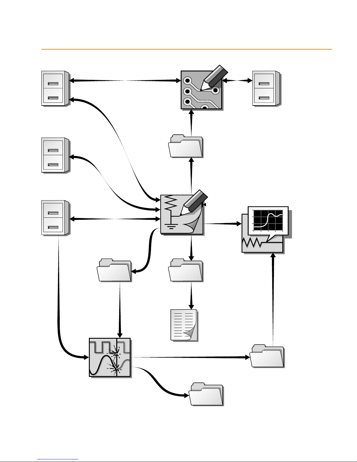
Figure 1 Interaction of Sim Software Programs and Files . . . . . . . . . . . . . . . 3
Figure 2 Opto-isolated, Addressable Serial-to-parallel Converter Circuit . . . . . . 5
Figure 3 Border Styles . . . . . . . . . . . . . . . . . . . . . . . . . . . . . . . . . . . 50
Figure 4 Placing Resistors with Various Vertical and Horizontal Offsets . . . . . . 96
Figure 5 Auto Naming for Bus Labels . . . . . . . . . . . . . . . . . . . . . . . . . . 98
Figure 6 Orthogonal Wire Drawing . . . . . . . . . . . . . . . . . . . . . . . . . . 109
Figure 7 Rubberbanding with Orthogonal enabled . . . . . . . . . . . . . . . . . 112
Figure 8 Rubberbanding with Orthogonal disabled . . . . . . . . . . . . . . . . . 112
Figure 9 Rubberbanded path showing a potential connection . . . . . . . . . . . 113
Figure 10 Off-page Port . . . . . . . . . . . . . . . . . . . . . . . . . . . . . . . . . . 114
Figure 11 Global Ports . . . . . . . . . . . . . . . . . . . . . . . . . . . . . . . . . . 114
Figure 12 Selection rectangle . . . . . . . . . . . . . . . . . . . . . . . . . . . . . . . 116
Figure 13 Printing with Auto-Fit Enabled . . . . . . . . . . . . . . . . . . . . . . . 142
Figure 14 Zoom Factor Set to 100% with Printer Configured in Portrait Mode . . 142
Figure 15 Zoom Factor Set to 200% with Printer Configured in Portrait Mode . . 143
Figure 16 User-definable Zoom Enabled in Portrait Mode . . . . . . . . . . . . . . 144
Figure 17 User-definable Zoom Enabled in Landscape Mode . . . . . . . . . . . . 145
Figure 18 Pin Types . . . . . . . . . . . . . . . . . . . . . . . . . . . . . . . . . . . . 191
Figure 19 Example of Diode Bridge Rectifier Symbol . . . . . . . . . . . . . . . . . 217
Figure 20 Top-level Schematic Drawing for CMOS Inverter . . . . . . . . . . . . . 244
Figure 21 Schematic of CMOS Inverter . . . . . . . . . . . . . . . . . . . . . . . . . 248
Figure 22 A Working Schematic and Two Checkpoint Schematics . . . . . . . . . 273
Figure 23 Entire Connector Symbol . . . . . . . . . . . . . . . . . . . . . . . . . . . 278
Figure 24 Single Pin Symbol . . . . . . . . . . . . . . . . . . . . . . . . . . . . . . . 278
Figure 25 Bill of Materials Report . . . . . . . . . . . . . . . . . . . . . . . . . . . . 286
Page 12

Figures
xii
Page 13

Tables
Table 1 Remaining Parts to be Placed . . . . . . . . . . . . . . . . . . . . . . . . . . 10
Table 2 Standard Schematics Toolbar . . . . . . . . . . . . . . . . . . . . . . . . . . 33
Table 3 Drawing Toolbar . . . . . . . . . . . . . . . . . . . . . . . . . . . . . . . . . 35
Table 4 Simulation Toolbar . . . . . . . . . . . . . . . . . . . . . . . . . . . . . . . 36
Table 5 Annotation Graphics Toolbar . . . . . . . . . . . . . . . . . . . . . . . . . 38
Table 6 Schematic Editor Function Keys . . . . . . . . . . . . . . . . . . . . . . . . 40
Table 7 Zoned Border Default Decimal Parameters . . . . . . . . . . . . . . . . . . 51
Table 8 Zoned Border Default Metric Parameters . . . . . . . . . . . . . . . . . . . 51
Table 9 Attribute Text Characteristics . . . . . . . . . . . . . . . . . . . . . . . . . 92
Table 10 Symbol Editor Toolbar Buttons . . . . . . . . . . . . . . . . . . . . . . . 154
Table 11 Symbol Editor Function Keys . . . . . . . . . . . . . . . . . . . . . . . . 157
Table 12 Display Characteristics . . . . . . . . . . . . . . . . . . . . . . . . . . . . 159
Table 13 Content Options . . . . . . . . . . . . . . . . . . . . . . . . . . . . . . . . 168
Table 14 Distinctions Between Connectors and Ports . . . . . . . . . . . . . . . . 277
Table 15 Supported Layout Packages and File Formats . . . . . . . . . . . . . . . 292
Table 16 .
lst File Format . . . . . . . . . . . . . . . . . . . . . . . . . . . . . . . . 308
Page 14

Page 15

Before you begin
Welcome
Orcad family products offer a total solution for your core
design tasks: schematic- and VHDL-based design entry;
FPGA and CPLD design synthesis; digital, analog, and
mixed-signal simulation; and printed circuit board layout.
What's more, Orcad family products are a suite of
applications built around an engineer's design flow—not
just a collection of independently developed point tools.
PSpice Schematics is just one element in our total solution
design flow.
PSpice Schematics is a schematic capture front-end
program with a direct interface to PSpice.
In one environment, you can do all of the following using
PSpice Schematics:
• design and draw circuits
• simulate circuits using PSpice
• analyze simulation results using Probe
Page 16

Chapter Before you begin
• graphically characterize simulation stimuli using the
fully integrated PSpice Stimulus Editor, so stimulus
definitions are automatically associated with the
appropriate symbols
• graphically characterize simulation models using the
fully integrated PSpice Model Editor utility, so model
definitions are automatically associated with the
appropriate symbols
• interface to PSpice Optimizer for analog circuit
performance optimization
• interface to PCB programs for printed circuit board
layout
PSpice Schematics is fully integrated with PSpice, giving
you the flexibility to work through your circuit design in
a consistent environment.
16
Page 17

How to use this guide
This guide is designed so you can quickly find the
information you need to use PSpice Schematics. To help
you learn and use PSpice Schematics efficiently, this
manual is separated into the following sections:
• Chapter 1 - Getting started
• Chapter 2 - Using Design Manager
• Chapter 3 - Using the schematic editor
• Chapter 4 - Creating and editing designs
• Chapter 5 - Using the Symbol Editor
• Chapter 6 - Creating and editing Symbols
• Chapter 7 - Creating and editing hierarchical designs
• Chapter 8 - Preparing your design for simulation
How to use this guide
• Chapter 9 - Using Design Journal
• Chapter 10 - Preparing your design for board layout
Symbols and conventions
Our printed documentation uses a few special symbols
and conventions.
Notation Examples Description
C+r Press C+r. Means to hold down the C key while
pressing r.
A, f, o From the File menu, choose Open (A, f,
o).
Monospace font
In the Part Name text box, type PARAM. Text that you type is shown in
Means that you have two options. You
can use the mouse to choose the Open
command from the File menu, or you
can press each of the keys in
parentheses in order: first A, then f,
then o.
monospace font. In the example, you
type the characters P, A, R, A, and
M.
17
Page 18

Chapter Before you begin
UPPERCASE In Capture, open CLIPPERA.DSN. Path and filenames are shown in
uppercase. In the example, you open
the design file named CLIPPERA.DSN.
Italics In Capture, save design_name.DSN. Information that you are to provide is
shown in italics. In the example, you
save the design with a name of your
choice, but it must have an extension of
.DSN.
Related documentation
In addition to this guide, you can find technical product
information in the online help, online books, and our
technical web site, as well as in other books. The table
below describes the types of technical documentation
provided with PSpice Schematics.
This documentation component . . . Provides this . . .
This online guide—
PSpice Schematics User’s Guide
Online help Comprehensive information for understanding and using
An online, searchable version of this guide, available when
choosing Online Manuals from the Orcad family program
group (on the Start menu).
the features available in PSpice Schematics.
You can access help from the Help menu in PSpice
Schematics, by choosing the Help button in a dialog box, or
by pressing 1. Topics include:
• Explanations and instructions for common tasks.
• Descriptions of menu commands, dialog boxes, tools on
the toolbar and tool palettes, and the status bar.
• Error messages and glossary terms.
• Reference information.
• Product support information.
You can get context-sensitive help for a error message by
placing your cursor in the error message line in the session
log and pressing 1.
18
Page 19

This documentation component . . . Provides this . . .
How to use this guide
Orcad family customer support at
www.orcad.com/technical/technical.asp
An Internet-based support service available to customers
with current support options. A few of the technical
solutions within the customer support area are:
• The Knowledge Base, which is a searchable database
containing thousands of articles on topics ranging from
schematic design entry and VHDL-based PLD design to
PCB layout methodologies. It also contains answers to
frequently asked questions.
• The Knowledge Exchange, which enables you to share
information and ideas with other users and with our
technical experts in a real-time online forum. You can
submit issues or questions for open discussion, search
the Knowledge Exchange for information, or send email
to another participant for one-on-one communication. A
list of new postings will appear each time you visit the
Knowledge Exchange, providing you with a quick
update of what's been discussed since your last visit.
• The Technical Library, which contains online customer
support information that you can search through by
category or product. You can find product manuals,
product literature, technical notes, articles, samples,
books, and other technical information. Additionally,
technical information can be obtained through
SourceLink, which is an online customer support
information service for users of Cadence software other
than Capture, Component Information System (CIS),
Express, Layout, or PSpice.
• The Support Connection, which allows you to choose to
either view and update existing incidents, or create new
incidents. The information is delivered directly to us via
our internal database. This service is only available to
customers with current maintenance or Extended
Support Options (ESOs) in the United States and
Canada.
• The Live Connection, which enables you to open access
to your computer to a Customer Support person, who
can then view your actions on your computer monitor
as you demonstrate the problem you're having. Live
Connection's two-way transmission can also let you
view the actions on the Customer Support person's
computer monitor, as he or she demonstrates a method
or procedure to help you solve your problem. To
participate in Live Connection, you need to contact a
Customer Support person, in order to obtain a support
number to grant you access to the Live Connection site,
and to set up a time to “meet online” using Live
Connection.
19
Page 20

Chapter Before you begin
20
Page 21

Getting Started
Overview
1
This chapter describes Schematics: what it is, what it can
do, and how you can use it.
This chapter has the following sections:
Using Schematics
and describes various functions.
Example—Drawing a Schematic
step-by-step example of creating a schematic.
on page 1-2 provides a broad overview
on page 1-4 provides a
Page 22

Chapter 1 Getting Started
Using Schematics
Schematics is a schematic capture front-end program that
provides a convenient system for:
• creating and managing circuit drawings.
• setting up and running simulations.
• evaluating simulation results using MicroSim Probe.
• creating netlists for external PCB layout packages.
An important prerequisite to building a schematic is
availability of proper symbols for assembly. Schematics
has extensive symbol libraries and a fully integrated
symbol editor for creating your own symbols or
modifying existing symbols.
The main functions of Schematics are:
• creating and editing designs
• creating and editing symbols
• creating and editing hierarchical designs
• preparing a design for simulation
• preparing a design for board layout
These primary functions are described in the following
chapters.
2
Page 23
Using Schematics
packages
symbols
models
package definitions
symbol
definitions
circuit
file
netlist &
simulation
directives
layout
netlist
file
PSpice
Schematics
component
description
file
PCB Layout
netlist &
packaging
information
footprints
layout ECO file
back
annotation
Probe
Probe
markers
Figure 1 Interaction of Sim Software Programs and Files
PSpice A/D
Bill of
Materials
reports
simulation
audit
Probe
data
file
simulation results
simulation
output file
3
Page 24

Chapter 1 Getting Started
Example—Drawing a Schematic
The following example demonstrates the basic drawing
features for drawing a schematic. It shows you how to:
• start the schematic editor and begin a new design.
• find out which libraries are configured for Schematics.
• place parts on a schematic.
• connect the part using wires and buses.
• label wires and buses.
• change reference designators and part values.
• move parts, wires and text.
• use ports on a schematic.
• place power and ground symbols on a schematic.
• save your design.
Follow this example to create the circuit shown in
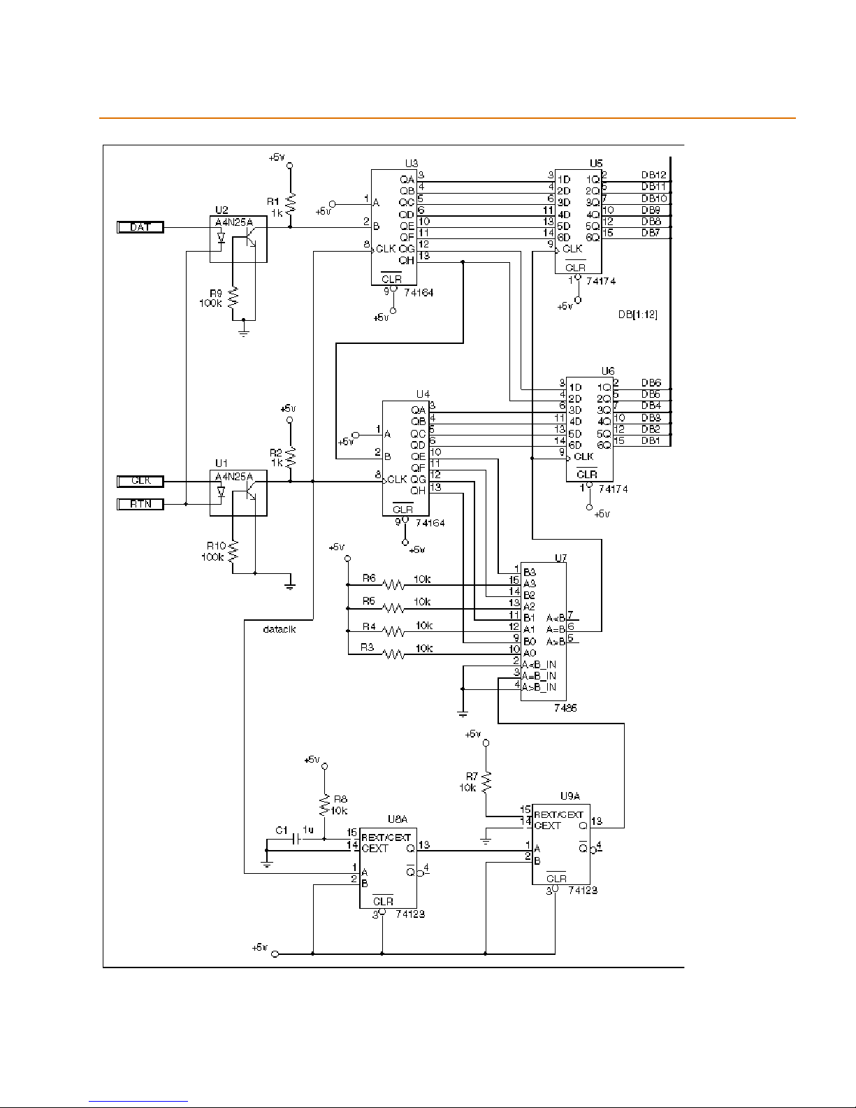
Figure 2.
4
Page 25
Example—Drawing a Schematic
Figure 2 Opto-isolated, Addressable Serial-to-parallel Converter Circuit
5
Page 26

Chapter 1 Getting Started
Starting a New Design
Start the schematic editor by double-clicking on the
Schematics icon in the Orcad program group. An empty
schematic page displays.
If you already have Schematics running with another
schematic displayed, click the New File icon to start a new
schematic.
Command Line Options
PSpice Schematics supports a number of command line
options that enable you to customize the start-up mode.
You can add one or more of these options to the
Command Line text box of the Program Item Properties
dialog box (File/Properties from within the Program
Manager) for the Windows Schematics program icon.
The command line options are:
Option Description
-i <filename.ini> activates Schematics using a specific file
(specified by <filename.ini>) for
configuration settings, rather than the
default: pspice.ini
-sym activates Schematics with a new Symbol
Editor document window
<filename> activates Schematics and loads the
schematic file specified by <filename.sch>
6
Page 27

Checking Symbol Libraries Configuration
When you installed Schematics, you selected a set of
libraries to be installed. These are global libraries, which
means the symbols contained in them are available to be
used in any new or existing schematic.
Check to see that you have the correct symbol libraries
configured for this example:
1 From the Options menu, select Editor Configuration.
Example—Drawing a Schematic
2 Check that the following libraries are included in the
Libraries list box:
7400 [.slb,.plb]
analog [.slb,.plb]
opto [.slb,.plb]
port [.slb]
1_SHOT [.slb]
Note If you are using the evaluation
version of Schematics, you will be using
“eval.slb”.
7
Page 28
Chapter 1 Getting Started
Th
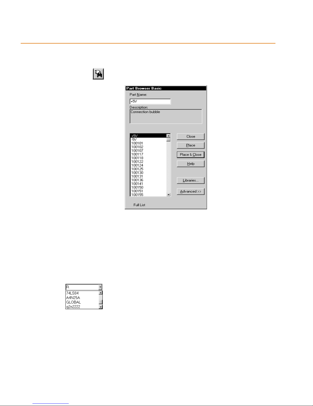
One of two Part Browser dialog boxes may
appear: the Part Browser Advanced or the
Part Browser Basic. If in the Part Browser
Advanced dialog appears, click <<Basic to
display the Part Browser Basic.
e Full List in the Part Browser dialog box
represents all the parts in the configured
symbol libraries that are available for your
use.
Selecting and Placing Parts
1 From the Draw menu, select Get New Part to display
the Part Browser dialog box.
Another method of selecting a part is to use
the Get Recent Part list box on the toolbar.
You can scroll and select a previously
placed part, or you can type the name of
the part you want to place.
2 There are several ways to select a part in the Part
Browser dialog box:
• If you know the name of the part, type the name in
the Part Name text box.
• Select the part name from the Full List of part
names.
• Click Libraries to view the Library Browser dialog
box, select a library, and select the part name from
that library’s list of parts.
3 Click Place to place the part (with the browser
remaining open) or click Place & Close (to place the
part and close the browser). If you leave the browser
open, click the title bar of the dialog box and drag it to
a new location.
8
Page 29
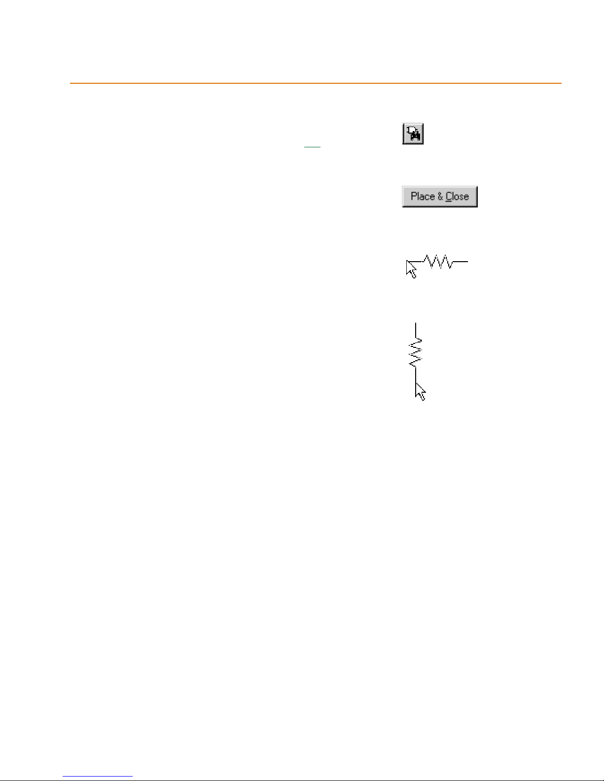
Placing resistors R1 and R2
1 From the Draw menu, select Get New Part to display
the Part Browser dialog box (shown on 1-8
).
Example—Drawing a Schematic
2 Type
R in the Part Name text box.
3 Click Place & Close.
The outline of the resistor becomes attached to the
pointer.
Note that as you move the pointer, the X and Y
coordinates at the left of the Status Bar (bottom of the
window) change. These coordinates show the location
of the pointer from origin 0,0 (upper left corner) to the
closest 0.01 inch (or closest mm if you are using a
metric page size).
4 Press C+R to rotate the resistor before placing it.
5 Move the pointer to the 2.40, 1.80 coordinates (within
a few hundredths of the inch is close enough) and click
to place the resistor on the schematic. If the
Stay-on-Grid option is enabled, parts are
automatically placed on the nearest grid point.
6 Move the pointer to 2.40, 3.90 and click again to place
the second resistor on the schematic.
7 Right-click to stop placing the part.
Placing resistors R3 through R6
You can quickly place resistors R3 through R6 using the
Auto-Repeat function.
1 From the Options menu, select Auto-Repeat to display
the Auto-Repeat dialog box.
a Set Horizontal Offset to 00.00 and Vertical Offset
to -00.20.
b Select the Enable Auto-Repeat check box.
c Click OK.
2 From the Get Recent Part list box on the toolbar, select
R.
As you place parts, the numerical portion of
the reference designator is automatically
assigned. For instance, if you place resistor
R2, the next resistor you place will be
designated R3.
9
Page 30

Chapter 1 Getting Started
Tabl
e 1 Remaining Parts to be
Placed
3 Place the pointer in the approximate position for the
placement of R3 and click to place the part.
4 Press M three times to place three more resistors
above the first.
Placing resistors R7 through R10
1 From the Get Recent Part list box on the toolbar, select
R.
2 Press C+R to rotate the resistor before placing it.
Reference
Designator
C1
U1
U2 A4N25
U3 74164
U4 74164
U5 74174
U6 74174
U7 7485
Part
Name
C
A4N25
3 Place four resistors in the approximate locations of R7,
R8, R9, and R10.
4 Right-click to stop placing resistors.
Placing the remaining parts on the schematic
1 Click the Get New Part button.
2 In the Part Browser dialog box, select each part listed
in Table 1 from the Part list box.
3 Place the part on the schematic in the approximate
location shown in Figure 2.
10
Page 31

Drawing and Labeling Wires
Draw the wire labeled dataclk to connect pin 8 (CLK) on
U3 and pin 1 (A) on U8A.
Drawing the dataclk wire
1 Click the Draw Wire button.
The pencil pointer indicates that you are ready to
draw a wire.
2 Click pin 8 of U3 to begin the wire.
3 Following the illustration in Figure 2, click where you
want each vertex of the wire. Each click ends a wire
segment and starts a new one.
4 Click pin 1 of U8A
Notice that the wire is now ended where you clicked
to place a pin. The pointer remains in the shape of a
pencil and you are ready to start another wire.
Example—Drawing a Schematic
5 Wire the rest of the schematic to the bus, except for the
wires of the right sides of U5 and U6.
6 Right-click to stop drawing wires.
Labeling the dataclk wire
Label the wire connecting the CLK pin of U3 to the A pin
of U8A.
1 Double-click any segment of the wire to display the
Set Attribute Value dialog box.
2 Type
3 Click OK.
dataclk in the LABEL text box.
11
Page 32

Chapter 1 Getting Started
Buses must be labeled. Examples of legal
bus names are:
DB[0-12]
DB[0:12]
DB[0..12]
DB0, DB1, CLK
Drawing and Labeling Buses
Draw the bus labeled DB[1-12].
Drawing the bus
1 Click the Draw Bus button.
The pointer is now shaped like a pencil (as it was when
you were drawing wires).
2 Click where you want to start the bus.
3 Click the pointer where you want to end the bus.
4 Right-click to stop drawing buses.
Labeling the bus
1 Double-click any segment of the bus to display the Set
Attribute Value dialog box.
2 Type DB[1-12] in the LABEL text box.
You can use the Auto-Repeat function to
place the wires that connect the pins to the
bus because the wires will be the same
length and fixed distances.
3 Click OK.
Connecting wires to the bus
1 From the Options menu, select Auto-Repeat to display
the Auto-Repeat dialog box.
a Set the Vertical Offset to 00.10.
b Ensure that Enable Auto-Repeat is enabled.
c Click OK.
2 Click the Draw Wire button and draw a wire from pin
2 of U5 to the bus.
3 Press M five times to place five more wires.
4 Click the Draw Wire button and draw a wire from pin
2 of U6 to the bus.
5 Press M five times to place five more wires.
12
Page 33

Example—Drawing a Schematic
Labeling the wires connected to the bus
You can use Auto-Naming to label a uniform collection of
wires.
1 From the Options menu, select Auto-Naming to
display the Auto Naming dialog box.
a In the Wire/Port Labels frame, select the Enable
Auto-Increment check box.
b In the Label Template text box, type
the label for the first wire in the series.
Wires will be labeled incrementally from DB1 and
up.
c Click OK.
2 Select the first (lower-most) wire to be labeled.
3 Press C+E to label the wire.
4 Repeat steps 2 and 3 for each wire segment, in the
order they are to be labeled (from bottom to top).
DB1, which is
Note Each wire connecting to a bus must
be labeled with the name of one of the
signals on the bus.
13
Page 34

Chapter 1 Getting Started
Changing Reference Designators and Part Values
Change part values and reference designators by
double-clicking them and typing a new value in the dialog
box.
Changing U8A to U9B
When you place a part on the schematic,
the part is automatically assigned a
reference designator and a gate (if it is a
multi-part component). For instance, when
you placed the 74123 part, it was assigned
something like U8A (that is, reference
designator U8 and gate A).
If you placed any of the components in an
order other than the sequential order
shown in Figure 2, use this feature now to
change the reference designators to match
the schematic in Figure 2.
1 Double-click U8A to display the Edit Reference
Designator dialog box.
2 Type
3 Type
4 Click OK.
U9 in the Package Reference Designator text box.
B in the Gate text box.
Changing R9 from 1 kohm to 100 kohm
1 Double-click 1k (next to resistor R9) to display the Set
Attribute Value dialog box.
2 Change 1k to 100k.
3 Click OK.
Now, change the value of R10 to 100k and the values of R3
through R8 to 10k.
14
Page 35

Moving Parts, Wires, and Text
Th
Move parts, wires, buses, and text by clicking to select
them, and dragging them to a new location. To maintain
connectivity when moving parts, wires, or buses, enable
the rubberbanding option.
Moving resistor R1 up one grid
Example—Drawing a Schematic
For information on how to enable the
rubberbanding option, see
Rubberbanding
on page 4-111.
1 Click the resistor to select it.
2 Drag the resistor up one grid.
3 Place the resistor at the new location.
Part values, reference designators, and other text can be
moved in the same way.
Moving the value of R10
1 Click the 100k value of the resistor.
The box outline around the value indicates that it is
selected.
The box outline around the resistor shows that the
resistor is the owner of the selected value.
2 Drag the value of the resistor to a new location.
The box representing the 100k value follows as you
move the pointer.
e color of the selected resistor is the color
specified for the Selection display layer in
the Display Preferences dialog box (see
Configuring Colors
page 3-63).
on
15
Page 36

Chapter 1 Getting Started
Placing Ports
Ports in Schematics identify signals that are inputs or
outputs to a schematic. Place ports in the same way that
you place other parts.
Placing the port
1 From the Draw menu, select Get New Part to display
the Part Browser dialog box (shown on page 8).
2 Click Libraries to display the Library Browser dialog
box.
16
3 In the Library list box, select port.slb.
4 In the Part list box, select GLOBAL (which is the name
of a global port symbol).
5 Click OK.
6 In the Part Browser dialog box, click Place & Close.
7 Move the pointer to the location for the DAT port and
click to place the part.
8 Right-click to stop placing ports.
Page 37

Labeling the port
1 Double-click the port symbol to display the Set
Attribute Value dialog box.
Example—Drawing a Schematic
2 Type
3 Click OK.
Now place two more ports and label them CLK and RTN
as shown in Figure 2.
DAT in the LABEL text box.
Placing Power and Ground Symbols
Power and ground symbols are types of global port
symbols in Schematics. The label on the port defines the
name of the power supply.
Placing +5-volt power supplies
1 Type +5V in the Get Recent Part list box on the toolbar.
2 Press R to select the part.
3 Move the pointer to the location of the +5V symbol
and click to place the symbol.
4 Move the pointer and click to place the other nine +5V
symbols.
5 Right-click to stop placing parts.
All signals tied to power supplies of the same name are
connected.
17
Page 38

Chapter 1 Getting Started
Placing ground symbols
1 In the Get Recent Part list box on the toolbar, type
EGND.
2 Press R to select the part.
3 Move the pointer to the location of the ground symbol
and click to place the symbol.
4 Move the pointer and click to place the other four
ground symbols.
5 Right-click to stop placing parts.
Saving Your Work
Click the File Save button, or select Save (or Save As) from
the File menu to save the schematic.
If this is a new design, you are prompted to enter a file
name where the new schematic will be saved.
18
Page 39

Using Design Manager
Overview
2
This chapter provides introductory information about the
Design Manager.
This chapter has the following sections:
Understanding Design Manager
purpose and uses for Design Manager.
Managing Your Files in the Workspace
what a workspace is and how to manage your files within
it.
Design Manager Functions
Manager functions and activities.
Starting the Design Manager
start the Design Manager.
Design Manager Help
Design Manager Help.
on page 2-25 describes where to find
on page 2-20 describes the
on page 2-22 explains
on page 2-23 describes Design
on page 2-25 describes how to
Page 40

Chapter 2 Using Design Manager
Understanding Design Manager
Design Manager allows you to browse, manage, archive,
and restore your design files.
When you open a design file, Design Manager searches
the Windows Explorer for the following information:
• the name of the top-level folder where the file is stored
• the names of all files within the top-level folder and its
sub-folders
• the names of files in folders outside the top-level
folder that are linked to files within the top-level
folder
Design Manager gathers this information, arranges and
displays it in categories that show the relationships of the
files to one another. For instance, all PSpice Schematics
.sch files are listed in the Design Entry Files category,
while all simulation
Simulation Results category. Hierarchical schematics are
shown as child schematics to the parents.
.dat and .out files are listed in the
20
Page 41

Understanding Design Manager
21
Page 42

Chapter 2 Using Design Manager
Managing Your Files in the
Workspace
Multiple workspaces, in their own windows,
can be open simultaneously for browsing
and file management activities.
Because categories are for display purposes
only, you cannot move or copy files from
one category type to another category
type.
Design Manager views a file’s top-level folder (as seen in
Windows Explorer) as a workspace and assigns it the name
of the top-level folder.
Although workspaces are actual folders, categories are
not. Categories only display files found after Design
Manager searches the top-level folder and its sub-folders,
making it easy for you to identify and manage them.
Dependent files (such as hierarchical sub-schematic and
symbol library files) that are stored outside the
workspace, show a reference to their location.
You can copy and move all files, or a selected sub-set, from
one workspace to another workspace. This principle
applies to deleting files as well. Because categories are for
display purposes only, you cannot move or copy files
from one category type to another category type.
Design Manager also provides cut, copy, paste, and delete
operations at an individual file level, that work similar to
the same functions in Windows Explorer.
When files are copied, moved, or saved to a workspace,
Design Manager automatically arranges their display into
the appropriate file-type categories. Windows Explorer
(when opened or refreshed) reflects the action taken in the
workspace.
22
Note To get the optimal use of Design Manager, it is recommended that
only files related to one design be stored in one top-level folder,
and therefore in one workspace. Also, because Design Manager can
perform operations on a design file and all of its dependent files
simultaneously, perform file management functions within Design
Manger, rather than Windows Explorer.
Page 43

Design Manager Functions
The following describes Design Manager functions and
activities:
General characteristics
• availability for use without other Orcad programs
running
• automatic categorization of design-related files, sorted
into file-type categories, within a workspace
• ability to have multiple workspaces, in their own
windows, open simultaneously
• two methods (view by Category and view by Name)
with which you can view and manage all files within
a selected workspace, as well as external references to
files outside the selected workspace
Design Manager Functions
File management
• copy, move, and delete all files (or optionally a
selected sub-set), from one workspace to another
• optionally cut, delete, copy, and archive all dependent
files
• cut, delete, copy, and paste files as similarly done in
Windows Explorer
• drag-and-drop functionality
• acceptance of files from Windows Explorer, through
commands or drag-and-drop
• ability to create top-level folders in Windows Explorer
from Design Manager
23
Page 44

Chapter 2 Using Design Manager
Archive and restore
• archive and restore to save a design and all of its
references, package files for shipment to another
location, save disk space, and localize externally
referenced and shared files into a selected workspace
24
Page 45

Starting the Design Manager
The Design Manager is automatically opened and
minimized when you open PSpice Schematics. You can
also open Design Manager to view and manage files
without first opening Schematics.
Opening the Design Manager outside of Schematics
1 On the task bar, click the Start button.
2 Point to Programs.
3 Point to the Orcad folder.
4 Click Orcad Design Manager.
Design Manager opens with the Category view in effect.
Starting the Design Manager
Hints and Tips
• To get optimal use of Design Manager, place only files
related to one design in one workspace.
• It is beneficial to perform file management functions
within Design Manger, rather than Windows
Explorer. Design Manager can perform operations on
a design file and all of its dependent files
simultaneously.
Design Manager Help
Refer to PSpice Schematics Help and Design Manager
Help for procedures on how to use Design Manager.
25
Page 46

Chapter 2 Using Design Manager
26
Page 47

Using the Schematic Editor
Overview
3
This chapter provides background information about the
schematic editor. To see specific step-by-step instructions
for creating a design, see Chapter 4,
Designs.
This chapter has the following sections:
Components of a Design
explains the components of a design.
Main Window
the schematic editor. This section describes the uses of
menus, the toolbar and toolbar buttons, the status line and
the keyboard.
Configuring PSpice Schematics
information on configuring the schematic editor to suit
your requirements.
Controlling the Display in PSpice Schematics
describes how to control the display and printing of layers
on page 3-32 describes the user interface to
on page 3-29 introduces and
on page 3-41 provides
Creating and Editing
on page 3-60
Page 48

Chapter 3 Using the Schematic Editor
of your schematic, in addition to specifying colors and
sizes.
Zooming and Panning in Schematics
on page 3-68 tells how to
zoom in and out of the drawing, refresh the screen
display, pan to various sections of the drawing and fit the
drawing to the page.
Using the Message Viewer
on page 3-73 describes the
Message Viewer that displays system messages and
explains the various displays and controls.
28
Page 49

Components of a Design
A schematic consists of:
• symbols
• attributes
• wires
• buses
• text items
Schematics can have either a flat or hierarchical structure,
depending on the way you decide to implement your
design.
Components of a Design
PSpice Schematics uses two basic types of
parts: primitive and hierarchical.
Parts
Parts are electrical devices that make up a circuit, such as:
• resistors
• operational amplifiers
• diodes
• voltage sources
• digital gates
The graphical representation of a part is a symbol.
Symbols are stored in symbol libraries.
Primitive parts are at the lowest level and
explicitly contain all of the information
required by the netlister. Most symbols in
the symbol libraries are primitive parts.
Hierarchical parts have the same
appearance as primitive parts. The
difference is that hierarchical parts
represent one or more levels of schematics
and primitive parts do not.
A hierarchical part is modified by pushing
into it from within the schematic editor or
symbol editor and editing the associated
schematic.
A primitive part is modified by editing its
graphics, pins, and attributes.
29
Page 50

Chapter 3 Using the Schematic Editor
w
T
Symbols
Symbols are the graphical representation of parts, ports,
and other schematic elements. They are grouped by
functionality into symbol libraries. Each symbol contains
a specific set of attributes that define the symbol. You can
edit these attributes as well as create new attributes.
Symbols can share similar attributes and graphics.
Hierarchical symbols represent schematics and are the
mechanism that you use to create hierarchical designs.
Ports
Ports are not physical connectors. If you
ant a specific pin (such as a DB25 pin) you
must use a symbol for such a connector
from the “connect.slb” symbol library.
Ports are symbols that form connecting points leading into
or out of the schematic page. Ports provide connectivity
between schematic pages and between levels of hierarchy.
They play an important role in determining names of
electrical nets.
Attributes
wo attributes of a resistor are PKGTYPE
(package type) and VALUE.
Attribute
Name
PKGTYPE = RC05
VALUE = 1K
Value
Parts, ports, wires (nets), buses, and most other symbols
have associated attributes. An attribute consists of a name
and an associated value. Attributes are used for Bill of
Materials reports, and simulation and layout netlists.
Annotations
Text, graphics, and annotation symbols are used to show
non-electrical information on the schematic, such as
comments and tables. Annotation symbols primarily
consist of text and graphics. Title blocks and page borders
are considered annotations. For more information on
adding annotations to your schematic, see Adding
Non-Electrical Information on page 4-126.
30
Page 51

Connections
Parts and ports contain one or more pins where
connections are made. Electrical connections are formed
by wire and bus segments joining pins and other wire and
bus segments. Connections are also formed by attaching
pins directly to pins. PSpice Schematics represents each
such electrical connection by a junction. Junctions are
made visible when three or more connected items
converge at the junction. Junctions are created and
removed automatically.
Some parts have hidden pins. Hidden pins are most often
used for power and ground connections to digital parts.
Hidden pins are not connected by wires and buses, but
rather through an attribute that names the net, which they
belong (the
IPIN(<pinname>)=<netname> attribute) to.
Components of a Design
31
Page 52

Chapter 3 Using the Schematic Editor
Main Window
When you start PSpice Schematics, a schematic editor
window opens and displays a single schematic page. You
have the option of opening additional schematic editor
windows. Use these windows to:
• display different schematics.
• display different portions of a single schematic page.
• display different pages of the same schematic.
• display different levels of hierarchy from the same
schematic.
• display a separate symbol editor window.
Note Drop-down menu items sometimes
appear dimmed. In some cases, you must
select an object first or perform some other
operation before you can choose
unavailable items.
Menus
The display and operation of the menus and submenus in
PSpice Schematics follows a standard Windows layout
and operation.
32
Page 53

Toolbars
T
T
T
Toolbar buttons provide shortcuts for performing
common actions. All toolbars are dockable, so they may
be moved to any location on the schematic.
Main Window
o “dock” toolbars:
1 Click anywhere on the toolbar (except
on the buttons).
Standard Schematics
The Standard Schematics toolbar provides shortcuts to
standard Windows commands.
Table 2 Standard Schematics Toolbar
Button Name Function Page
New File opens a new schematic file
Open File opens an existing schematic
file
Save File saves a schematic file 4-14
Print
(immediate)
Cut deletes a selected object and
Copy copies a selected object to the
prints the active schematic 4-14
copies it to the clipboard
clipboard
4-79
4-79
6
0
4-11
9
4-11
9
2 Drag it to the desired location in the
schematic window or on your desktop.
he next time you open Schematics, the
toolbars will be where you last placed them.
o display toolbars:
1 From the View menu, select Toolbars.
2 Select or clear the check box for each
toolbar to enable or disable its display.
3 Click Close and the selected toolbars
will display.
Paste pastes the most recently cut
or copied object from the
clipboard
Undo undoes the previous action 4-12
Redo redoes what was just undone 4-12
4-11
9
0
0
33
Page 54

Chapter 3 Using the Schematic Editor
Table 2 Standard Schematics Toolbar
Button Name Function Page
Redraw refreshes the active schematic
page screen display
Zoom In views a smaller area of
schematic
Zoom Out views a larger area of
schematic
Zoom Area views a selected area of
schematic
Zoom to Fit Page fits the view to show all items
on the page
3-41
3-68
3-69
3-68
3-70
34
Page 55

Drawing
The Drawing toolbar provides shortcuts for drawing and
editing items on your schematic.
Table 3 Drawing Toolbar
Button Name Function Page
Main Window
Draw Wire enables drawing of wires
on the schematic
Draw Bus enables the drawing of
buses on the schematic
Draw Block enables the placing of
blocks on the schematic
Get New Part displays Part Browser
dialog box for selecting
parts for placement
Get Recent
Part
Edit Attributes edits the attributes of
Edit Symbol opens the symbol editor
drop-down list box to
select and place a recent
part without having to
open the part browser
selected objects
for the selected symbol
4-10
4
4-10
7
7-22
8
4-82
4-85
4-93
5-15
1
Note You can also type the name of the
part directly into the text box.
35
Page 56

Chapter 3 Using the Schematic Editor
Simulation
The Simulation toolbar provides shortcuts for setting up
analyses, running a simulation, and viewing results.
Refer to the Viewing Results on the Schematic chapter of
your PSpice A/D User’s Guide for further information on
simulation in Schematics.
Table 4 Simulation Toolbar
Button Name Function Page
Analysis Setup sets up simulation
analyses for the active
schematic
Simulation starts a simulation of the
current schematic
Marker Color drop-down list box to
change marker colors on
an instance basis
Voltage/Level
Marker
Current Marker enables placing of
enables placing of
voltage/level markers
on the schematic
current markers on the
schematic
8-2
60
8-2
66
*
*
*
36
Page 57

Table 4 Simulation Toolbar
Button Name Function Page
Main Window
Enable Bias
Voltage Display
Show/Hide
Voltage on
Selected Net(s)
Enable Bias
Current Display
Show/Hide
Currents on
Selected Part(s)
* Refer to the Viewing Results on the Schematic chapter in your PSpice user’s
guide for information about how to use these toolbar buttons.
toggles the display of
bias voltage
toggles the display of
voltages for selected
wires
toggles the display of
bias current
toggles the display of
currents for selected
device pins
*
*
*
*
37
Page 58

Chapter 3 Using the Schematic Editor
Annotation Graphics
The Annotation Graphics toolbar provides shortcuts for
drawing or inserting non-electrical information onto your
schematic.
Table 5 Annotation Graphics Toolbar
Button Name Function Page
Draw Arc draws an arc shape on the
page
Draw Box draws a box on the page 6-17
6-17
8
8
Draw Circle draws a circle on the page 6-17
9
Draw
Polyline
Draw Text places of a single line of
draws a polyline on the
page
text on the page
6-17
9
4-12
9,6-1
80
Draw Text
Box
Insert
Picture
places multiple lines of text
on the schematic
places a bitmap (.bmp,
.dib) or Windows metafile
(.wmf) on the page
4-12
6
4-13
3
38
Page 59

Status Bar
The status bar is located at the bottom of the schematic
editor window and provides the following:
• X and Y coordinates of the pointer.
Use the Display Options selection under the Options
menu to toggle display of X and Y coordinates.
• A message area that provides:
• a brief description of the function that will be
performed if you click the toolbar button at the
present pointer location.
• a brief description of the function to be performed.
The description will display by selecting the menu
item at the present pointer location.
• prompts and warning messages that only appear
when it is necessary for you to take a specific
action.
Main Window
If anything must be done by the user or if there is
a warning, the prompt will display in the status
bar.
• the name of the function to be performed when you
use the Repeat command (the name of the function
will display when you use the Repeat function).
Use the Status Bar selection from the View menu to enable
or disable the status bar.
Refreshing the Screen
To refresh the screen, click the Redraw button on the
toolbar.
Keyboard
Table 6 lists the function keys in the schematic editor that
permit you to enable or disable specific commands.
39
Page 60

Chapter 3 Using the Schematic Editor
Table 6 Schematic Editor Function Keys
Key Action Menu Selection
1 Online Help Help Help
Function keys 4 through 9 are
toggle keys. Pressing the key enables the
feature, and pressing S plus the
key disables the feature.
2 Move to lower level in
the schematic hierarchy
3 Move up one level
in the schematic
hierarchy
4 Text stay-on-grid Options Display
5 Orthogonal Options Display
6 Stay-on-grid Options Display
7 Auto-increment Options Auto-Na
8 Auto-repeat Options Auto-Rep
9 Rubberbanding Options Display
Navigate Push
Navigate Pop
Options
Options
Options
ming
eat
Options
40
0 View errors, warnings,
and messages
! Start the simulator Analysis Simulate
@ Start MicroSim Probe Analysis Run
File View
Messages
Probe
Page 61

Configuring PSpice Schematics
The following list summarizes the different types of
options you can configure in PSpice Schematics.
Customizing configurable options allows you to use
PSpice Schematics in the way that best suits your needs
and requirements.
Library settings
• changes the set of configured symbol libraries
Page settings
• sets the page size for your schematic
• specifies other page settings such as paper size, pin
spacing, and borders
Configuring PSpice Schematics
Display options and preferences
• changes the grid and gravity settings of the schematic
editor
• sets the time interval between automatic saves of your
schematics
• changes the font used for displaying and printing text
on your schematics
• determines which elements of a schematic are to be
displayed and printed
• changes the colors used for drawing and displaying
objects
Application settings
• specifies the number of items in the Get Recent Part
list box on the toolbar
• changes where to find the .exe files for programs that
interface with PSpice Schematics and which
initialization file to use other than the installed default
initialization file (pspice.ini)
• specifies the use of a different text editor
41
Page 62

Chapter 3 Using the Schematic Editor
Configuring Symbol Libraries
There are two major elements that work together in
Schematics that let you place symbols into your design:
• symbol libraries
• library search list
Symbol libraries are located in library directories. The
library search list is in the Part Browser and the Editor
Configuration dialog box under the Options menu.
A library name must be in the library
search list to be available for placing its
symbols.
It is important to remember that libraries and the search
list have two distinct functions. You can create a symbol
library, but if the library name is not in the library search
list, it is not available to the design for placing symbols.
Conversely, you can inadvertently create an error
condition by having a library name in the search list, for a
library that doesn’t exist.
Configuring a symbol library is adding a library name to
the library search list.
Note When adding a symbol library to the library search list, placement
in the list is important. If more than one library contains the same
symbol name, Schematics uses only the first one it encounters.
You must ensure the library actually exists in the location
specified during the configuration procedure.
42
Page 63

Types of Libraries
Schematics recognizes two types of libraries:
This library... Is available...
global to all schematic designs. They are listed
in the pspice.ini file and are
automatically loaded into the library
search list for every design.
Global libraries appear in the library
search list with an asterisk (*) preceding
the library name.
local to designs within which they are saved.
Schematics always places local library
names at the top of the library search
list. Local libraries are always searched
first.
Configuring PSpice Schematics
Default Library Directory
Schematics includes a default library directory where all
the symbol libraries (.
reside. It is not required to configure these libraries. They
are already configured in the search list as global libraries.
However, if you prefer, you can:
• change the order in which libraries appear in the
search list, thereby changing the order in which they
are searched
• remove library names from the search list (without
deleting the libraries)
• add new libraries
• delete libraries
• reconfigure libraries from global to local
slb) you selected during installation
Note To maintain the integrity of your
default symbols, we recommend making a
copy of the default symbol libraries. If you
use the symbol editor to make changes to a
default symbol, it will overwrite the default
symbol if you save using the default file
name. Also, if you import symbol files into
the default library and an imported file has
the same name as the default file, the
imported file will overwrite the default file.
43
Page 64

Chapter 3 Using the Schematic Editor
User-Defined Symbol Libraries
You can create global and local symbol libraries, and add
them to the default directory or to another directory of
your choice. Once created, you can perform all the same
actions as listed in Default Library Directory
on page 3-43.
Note When adding a symbol library to the library search list, placement
in the list is important. If more than one library contains the same
symbol name, Schematics uses only the first one it encounters.
If you add local library names to the library search list,
Schematics places them before global library names,
because they are searched first. You can control their
placement within a group of local library names, but you
cannot integrate them into the global names.
Adding a library
Options Menu
1 From the Options menu, select Editor Configuration
to display the Editor Configuration dialog box.
2 Click Library Settings to display the Library Settings
dialog box.
44
Page 65

3 In the list of libraries, select the location for the new
library.
A new global library will be added directly above the
library you select. A new local library will be placed
above the first global library name in the list.
Configuring PSpice Schematics
4 If the library you are adding is a symbol library, select
the Symbol check box. If the library you are adding
has an associated package library, select the Package
check box.
5 In the Library Name text box, type the name of the
library.
Do not type a file name extension if the library you are
using is listed in the dialog box; the file name
extension is appended automatically.
6 Click Add* for a global library, or click Add Local for
a local library.
If you are adding a global library, Schematics writes
the library name to the pspice.ini file so it is
available to all schematic designs.
7 Click OK to exit the Library Settings dialog box.
8 In the Editor Configuration dialog box, click OK.
If the library you are using is stored
elsewhere, the full path must be entered.
45
Page 66

Chapter 3 Using the Schematic Editor
T
Removing Library Names
When removing a library name, it is only
removed from the configured libraries list.
he library is not deleted.
Options Menu
If you no longer need a library name in the list of
configured libraries, you can remove it from the list of
configured libraries.
Removing a library name
1 From the Options menu, select Editor Configuration
to display the Editor Configuration dialog box (shown
on 3-44
2 Click Library Settings to display the Library Settings
dialog box (shown on 3-45).
3 In the list of libraries, select the library name that you
want to remove.
The selected library name is displayed in the Library
Name text box.
4 Click Delete.
5 Click OK to exit the Library Settings dialog box.
6 In the Editor Configuration dialog box, click OK.
).
46
Correcting Library Names
If you type a library name incorrectly, you can change the
name as it appears in the list of configured libraries.
Correcting a library name
1 From the Options menu, select Editor Configuration
to display the Editor Configuration dialog box (shown
on 3-44
2 Click Library Settings to display the Library Settings
dialog box (shown on 3-45
3 In the list of libraries, select the library that you want
to change.
The name of the selected library displays in the
Library Name text box.
4 In the Library Name text box, type a new name for the
library.
).
).
Page 67

Do not type a file name extension; the file name
extension is appended automatically.
5 Click Change.
6 Click OK to exit the Library Setting dialog box.
7 In the Editor Configuration dialog box, click OK.
Changing the Search Order
The way that PSpice Schematics searches libraries for a
symbol follows the order in which the libraries are
configured in the list. You can change the position of a
library in the list.
Configuring PSpice Schematics
Changing the position of the library in the list
1 From the Options menu, click Editor Configuration to
display the Editor Configuration dialog box (shown
on 3-44
2 Click Library Settings to display the Library Settings
dialog box (shown on 3-45).
3 In the list of libraries, select the library name that you
want to move.
The name of the selected library displays in the
Library Name text box.
4 Click Delete.
5 In the list of libraries, select the name above which the
repositioned name will be inserted.
6 In the Library Name text box, type the name of the
library you want to reposition.
Do not type a file name extension; the file name
extension is appended automatically.
).
Options Menu
7 If the library is a symbol library, select the Symbol
check box. If the library has an associated package
library, select the Package check box.
8 Click Add* for a global library or click Add Local for a
local library.
47
Page 68

Chapter 3 Using the Schematic Editor
The repositioned library name is inserted above the
selected name.
9 Click OK to exit the Library Setting dialog box.
10 In the Editor Configuration dialog box, click OK.
Changing the Search Path
Note Local libraries are first looked for in
the directory where the schematic resides.
PSpice Schematics looks for a library according to the
path(s) specified by the Library Path in the Editor
Configuration dialog box.
Changing the library search path
1 From the Options menu, select Editor Configuration
to display the Editor Configuration dialog box.
48
2 Type a new path or add to the existing path in the
Library Path text box.
Specify multiple directories by separating them with a
semicolon:
c:\msim\lib
c:\msim\lib;c:\project\lib
3 Click OK.
Page 69

Changing Page Size
PSpice Schematics supports standard page sizes A
through E and A0 through A4. It also allows you to specify
a user defined page size.
Changing the page size
Configuring PSpice Schematics
1 From the Options menu, click Page Size to display the
Page Size dialog box.
2 Click the appropriate button to select a pre-defined
page size, or indicate a User Defined Size by typing the
page dimensions in the Horiz: and Vert: text boxes.
3 Click OK to change the page size of the currently
active page and to establish the default page size for
all later pages.
Options Menu
49
Page 70

Chapter 3 Using the Schematic Editor
Note If you are using zoned borders,
make sure the Display check box for the
Page Boundary layer in the Display
Preferences dialog box is enabled (see
Controlling the Display in
PSpice Schematics on
page 3-60).
Changing Page Settings
For all page sizes, you can change the border style, the
drawing area, and the pin-to-pin spacing.
Border Style
Schematics provides two border styles: zoned and outline.
Figure 3 illustrates the two styles.
Zone
designator
Note Drawing areas for the zoned and
outline border types are the same size, as
shown in Figure 3.
Drawing
area
Drawing
area
zoned border
outline border
Margin
Figure 3 Border Styles
You can configure a zoned border for all decimal and
metric page sizes, including custom sizes (see Changing the
border style on page 3-52.)
The following table lists the default decimal page sizes
and their configurations.
50
Page 71

Table 7 Zoned Border Default Decimal Parameters
Configuring PSpice Schematics
Type Dimension*
A 8.5 x 11 2 .25 2 .38
B 11 x 17 2 .62 4 .38
C17 x 224.5 4.75
D22 x 34 41.0 8 .5
E34 x 448.5 81.0
* in inches
Vertical Horizontal
Zones Margin Zones Margin
The following table lists the default metric page sizes and
their configurations.
Table 8 Zoned Border Default Metric Parameters
Type Dimension*
Vertical Horizontal
Zones Margin Zones Margin
A4 210 x 297 2 6.35 2 9.65
A3 297 x 420 2 15.75 4 9.65
A2 420 x 594 4 12.7 4 19.5
A1 594 x 841 4 25.4 8 12.7
A0 841 x 1189 8 12.7 8 25.4
* in millimeters
Note If your design doesn’t require a zoned border, Outline Border will
display the page with fewer details.
51
Page 72

Chapter 3 Using the Schematic Editor
Changing the border style
You can specify which border style to use through the
Editor Configuration dialog box. The current drawing and
all subsequent new drawings use the style you select.
Options Menu
1 From the Options menu, select Editor Configuration
to display the Editor Configuration dialog box.
2 Click Page Settings to display the Page Settings dialog
box.
52
3 Select the page size for which you want to set the
border style.
You can select either style for each page size.
Page 73

Configuring PSpice Schematics
T
4 Select the Outline or Zoned border style.
For style... Do this...
Outline
1 In the Borders frame, click the
Outline button.
2 Click OK to accept the Outline
border and exit the Page Settings
dialog box.
Zoned
1 In the Borders frame, click the
Zoned button.
2 Type the number of zones for each
axis.
3 Type the margin sizes for each axis.
4 Select letters or numbers for zone
designators in each plane.
5 Select Ascending or Descending (in
reference to the upper-left corner of
the page), in each plane.
o round the corners on the outside border
line, select the Rounded Corners check box.
6 Click OK to accept the Zoned
border and exit the Page Settings
dialog box.
Note Line widths for the page boundary are specified in the Display
Preferences dialog box. See Setting the default graphics
properties through Display Preferences on page 4-132
for more information.
53
Page 74

Chapter 3 Using the Schematic Editor
Drawing Area
Changing the drawing area size
1 From the Options menu, select Editor Configuration
to display the Editor Configuration dialog box (shown
on 3-52
2 Click Page Settings to display the Page Settings dialog
box.
).
Note Drawing areas for zoned and outline
border types are the same size, (see
Figure 3 on page 3-50).
54
3 In the Width and Height text boxes, type the drawing
area dimensions for the page size.
4 Click OK to exit the Page Settings dialog box.
5 In the Editor Configuration dialog box, click OK.
Page 75

Pin-to-Pin Spacing
You can scale symbols so they will appear larger or
smaller on the schematic. You do this by changing the
pin-to-pin spacing for a given page size.
Changing the pin-to-pin spacing
1 From the Options menu, select Editor Configuration
to display the Editor Configuration dialog box (shown
on 3-52
2 Click Page Settings to display the Page Settings dialog
box (shown on 3-54).
3 In the Pin-to-Pin Spacing text box, type a new value.
4 Click OK.
).
Configuring PSpice Schematics
Changing Grid and Gravity
The grid and gravity functions of PSpice Schematics ease
your drawing tasks and can help make your schematic
more precise.
Grid On
When Grid On is enabled, the grid is displayed in the
drawing area of the schematic editor window.
Enabling or disabling the grid display
1 From the Options menu, select Display Options.
2 Select or clear the Grid On check box to enable or
disable the grid display.
3 Click OK.
55
Page 76

Chapter 3 Using the Schematic Editor
Stay-on-Grid
Stay-on-grid controls the method of object placement.
When Stay-on-Grid is enabled, the objects are forced onto
grid when placed. We recommend that you enable this so
that electrical connections are made correctly.
Enabling or disabling stay-on-grid
1 From the Options menu, select Display Options.
2 Select or clear the Stay-on-Grid check box to enable or
disable Stay-on-Grid.
3 Click OK.
Snap-to-Grid
Snap-to-grid controls the movement of the object while
being moved for placement when Stay-on-Grid is
enabled. If Snap-to-Grid and Stay-on-Grid are both
enabled, movement during object placement is in
increments equal to the current grid spacing. If
Snap-to-Grid is not selected, the object moves smoothly.
Note The Stay-on-Grid command must be
enabled for the Snap-to-Grid command to
be effective.
Enabling or disabling snap-to-grid
1 From the Options menu, select Display Options.
2 Select or clear the Snap-to-Grid check box to enable or
disable snap-to-grid.
3 Click OK.
56
Page 77

Snap-to-Pin
Snap-to-pin, when enabled, causes the endpoint of a wire
or bus segment to snap to the nearest pin if one is found
inside the radius defined by the Gravity setting.
Enabling or disabling snap-to-pin
1 From the Options menu, select Display Options.
2 Select or clear the Snap-to-Pin check box to enable or
disable snap-to-pin.
3 Click OK.
Grid Spacing
Grid Spacing defines the horizontal and vertical grid
spacing on your drawing area. The default spacing is 10
units. This corresponds to (and displays as) 0.10 inches for
US-standard page sizes, and 2.5 millimeters for metric
page sizes. The minimum grid spacing allowed is 0.01
inch, or .25 millimeters.
Configuring PSpice Schematics
Specifying grid spacing
1 From the Options menu, select Display Options.
2 In the Grid Spacing frame, type the grid spacing value.
3 Click OK.
Gravity
The gravity setting specifies how close an object must be
to a pin to snap to it. Gravity is only functional when
snap-to-pin is enabled.
Specifying gravity
1 From the Options menu, select Display Options.
2 In the Snap-to-Pin frame, type the snap-to-pin gravity
value.
3 Click OK.
Gravity is only functional when snap-to-pin
is enabled.
57
Page 78

Chapter 3 Using the Schematic Editor
Text Grid
Text Grid allows you to set the grid spacing for text
separately from the drawing grid spacing. The text grid is
usually set to some smaller percentage of the drawing
grid. This allows you to align text between drawing grid
points.
Enabling text grid and specifying text grid size
1 From the Options menu, select Display Options.
2 In the Text Grid frame, select the Stay-on-Grid check
box to enable the text grid.
3 In the Grid Size text box, type the text grid spacing
value.
4 Click OK.
Setting the Autosave Interval
The autosave interval specifies the time interval, in
minutes, which PSpice Schematics automatically saves
any modified schematics or libraries.
Setting the Autosave interval
1 From the Options menu, select Editor Configuration
to display the Editor Configuration dialog box.
2 In the Autosave interval box, type the number of
minutes for the autosave interval.
3 Click OK.
58
Page 79

When Autosave is enabled, PSpice Schematics creates a
temporary file with the same name as the active working
file, and a file name extension ending in ‘
v’ (for example,
“.scv,” “.slv,” “.plv”). If you have a power outage or
system failure, you can retrieve your work from these
files.
The temporary files are deleted each time a schematic or
library is successfully closed or saved. When you open a
file, PSpice Schematics compares the saved file to the
autosave file, if one is present. If the autosave file is more
recent than the requested file, PSpice Schematics provides
a warning and allows you to restore the file as the active
schematic or library.
While an autosave is in progress, a message appears in the
status line and the hourglass symbol displays in place of
the pointer. Wait until the autosave is finished before
continuing.
Configuring PSpice Schematics
Disabling Autosave
1 From the Options menu, select Editor Configuration
to display the Editor Configuration dialog box (shown
on 3-48
2 In the Autosave interval text box, type 0 (zero).
3 Click OK.
).
59
Page 80

Chapter 3 Using the Schematic Editor
Controlling the Display in PSpice
Schematics
PSpice Schematics allows you to define what elements of
a design you want to display and print. This means you
can set different display properties for each element of
your schematic. In the Display Preferences dialog box, the
default colors, styles, fonts, and sizes of each display layer
are established.
You can either display or not display (and print or not
print) the following:
Annotation Graphics Attribute Text Buses
Hidden Pins Junctions Labels
Markers and
Viewpoints
Pin Names Pin Numbers Ports
Reference
Designators
Stimulus Symbol Text Symbols
Text Text Box Title and Border
User-specified text Wires
Page Boundary Part Names
Simulation Currents Simulation
Voltages
60
Page 81

Displaying or printing default properties
T
T
1 From the Options menu, select Display Preferences to
display the Display Preferences dialog box.
Controlling the Display in PSpice Schematics
Options Menu
2 From the Display Layers list, select the appropriate
display layer (or layers).
3 Click the General tab.
4 Select or clear the Display check box to enable or
disable display of the selected layers.
5 Select or clear the Print check box to enable or disable
o select more than one layer
consecutively:
1 Hold down S.
2 Click the first desired layer in the list
and the last.
Every layer in between will be selected.
printing of the selected layers.
6 Click Apply to apply the changes and keep the dialog
box displayed for further changes, or click OK to
apply the changes and close the dialog box.
o select more than one layer
non-consecutively:
1 Hold down C.
2 Click each desired layer.
61
Page 82

Chapter 3 Using the Schematic Editor
T
If you are rotating text objects, use
rueType fonts to prevent the display from
becoming distorted.
Options Menu
Changing Fonts
To change the default fonts PSpice Schematics uses to
display and print text, use the Display Preferences dialog
box.
Selecting a font
1 From the Options menu, select Display Preferences to
display the Display Preferences dialog box.
2 Select one or more layers from the Display Layers list.
3 Click the Text tab.
4 Click Browse to display the Font dialog box.
62
Page 83

5 Select a font and size from their corresponding list
boxes and click OK.
A sample of the selected font is shown in the Sample
box.
6 Enter a size in either inches or millimeters, or accept
the system default for the selected font.
7 Select a color from the Color list box.
8 Click Apply to apply the changes and keep the dialog
box displayed for further changes, or click OK to
apply the changes and close the dialog box.
Configuring Colors
The colors for all layers in Schematics are configured in
the Display Preferences dialog box. The colors you specify
become the defaults, however, they may be changed as
often as necessary.
Controlling the Display in PSpice Schematics
Configuring Colors in your Schematic
1 From the Options menu, select Display Preferences to
display the Display Preferences dialog box (shown on
page 3-62
2 Select one or more layers from the Display Layers list.
3 Click the tab that applies to the layers you have
selected.
For example, if you want to change a text color, select
the layer, click the Text tab, and select the appropriate
display settings.
4 Select a color from the Color drop-down list.
5 Click Apply to apply the changes and keep the dialog
box open for further changes, or click OK to apply the
changes and close the dialog box.
).
63
Page 84

Chapter 3 Using the Schematic Editor
Changing Application Settings
You have the option to change the location of the .exe files
of the programs that Schematics interfaces with. You can
also configure a different text editor (besides WordPad)
and specify an initialization file other than the installed
default initialization file.
Changing where to find programs
1 From the Options menu, select Editor Configuration
to display the Editor Configuration dialog box.
64
2 Click App Settings to display the App Settings dialog
box.
Page 85

Controlling the Display in PSpice Schematics
w
T
The Simulate Command frame shows the path that
PSpice Schematics uses to run MicroSim PSpice A/D.
3 To change the path name, type a new path name in the
Command text box.
Note The Simulate Command frame will
show either PSpice or PSpice A/D,
depending on the package that you have
purchased. If you are using a network
licensed version that has both PSpice and
4 Similarly, to change any of the other command lines,
click to select the command in the Other Commands
PSpice A/D available, you can choose
hich simulator you want to use.
list box and type a new path name in the Command
text box.
5 Click OK to exit the App Settings dialog box.
6 In the Editor Configuration dialog box, click OK.
Changing the configuration file
A configuration file other than the default pspice.ini
file can be used for any of the programs that Schematics
interfaces with.
1 From the Options menu, select Editor Configuration
to display the Editor Configuration dialog box (shown
on 3-65
).
2 Click App Settings to display the App Settings dialog
box (shown on 3-65
).
3 In the Configuration File frame, select Other.
o change the configuration file for PSpice
Schematics:
1 In the Windows Program Manager,
select the PSpice Schematics icon.
2 Select Properties from the File menu.
3 Append -i<configuration file name> to
the Command Line.
4 Click OK.
65
Page 86

Chapter 3 Using the Schematic Editor
4 Type the file name of the configuration file in the text
box.
5 Click OK to exit the App Setting dialog box.
6 In the Editor Configuration dialog box, click OK.
Specifying a different text editor
Editing text in PSpice Schematics is done through the
WordPad program. You have the option to specify a
different text editor.
1 From the Options menu, select Editor Configuration
to display the Editor Configuration dialog box (shown
on 3-65
).
2 Click App Settings to display the App Settings dialog
box (shown on 3-65
).
3 In the Other Commands box, select Text Editor.
4 Type a new path name in the Command text box to
specify the path and name of the text editor you want
to use.
5 Click OK to exit the App Settings dialog box.
6 In the Editor Configuration dialog box, click OK.
66
Page 87

Changing the Get Recent Part List Size
The Get Recent Part list box on the toolbar contains a
scroll-down list of recently placed parts. The default
length of this list is ten items.
To change the length of the list, use a text editor to edit the
MRPLISTSIZE item in the [SCHEMATICS] section of the
pspice.ini file.
MRPLISTSIZE=<length of list>
Controlling the Display in PSpice Schematics
67
Page 88

Chapter 3 Using the Schematic Editor
Zooming and Panning in
Schematics
Zooming
When working on a design, you can zoom in (enlarge the
view) or zoom out (reduce the view) to view a larger or
smaller portion of the schematic window. Zooming in
reduces the area viewed and enlarges the objects viewed.
Zooming out increases the area viewed and reduces the
size of the objects viewed.
Zooming in
or press C+I
or press C+A
1 From the View menu, select In.
2 Move the pointer to the desired center of the zoom
action and click.
Zooming in about the center of the window
1 Click the Zoom In button.
The amount of magnification is determined by the
Zoom Scale Factor (see Setting Zoom Parameters
page 3-69).
on
Zooming in on a selected area of the page
1 Click the Zoom Area button, or select Area from the
View menu.
2 Drag a selection rectangle to select the desired display
area.
Zooming out
or press C+O
68
1 From the View menu, select Out.
2 Move the pointer to the desired center of the zoom
action and click.
Page 89

Zooming out about the center of the window
Zooming and Panning in Schematics
1 Click the Zoom Out button.
The amount of reduction is determined by the Zoom
Scale Factor (see Setting Zoom Parameters
on page 3-69).
Zooming out to view the full schematic page
1 From the View menu, select Entire Page.
Setting Zoom Parameters
Setting scale factor and fit
The Zoom parameters tailor how the work space will be
magnified or reduced when you make selections from the
View menu, or click any of the zoom buttons.
1 From the Options menu, select Pan & Zoom to display
the Pan & Zoom dialog box.
or press C+O
or press C+N
Options Menu
2 In the Scale Factor text box, type a value.
This value defines the factor by which the screen is
magnified or reduced when you select Zoom In or
Zoom Out. A Scale Factor of 2 will double (or halve)
the size of objects viewed.
3 In the Fit text box, type a value.
69
Page 90

Chapter 3 Using the Schematic Editor
or press C+N
This value defines the percentage of the work space to
be filled with the complete schematic when you select
View Fit. Type a decimal value between 50 and 100. A
typical value is 90.
4 Click OK.
Fitting to a Page
All of the parts, wires and text within the active window
(excluding the title block) are displayed by fitting the view
to the page.
Fitting the view to the page
1 Click the Zoom to Fit Page button, or select Fit from
the View menu.
View Menu
Panning
Panning allows you to select a new window centering
point. The current zoom scale remains the same. When
you select the new center point, the schematic is panned
until the selected point is in the center of the window.
Panning to a new center
1 From the View menu, select Pan—New Center.
2 Move the pointer to the desired window center and
click.
70
Page 91

Automatic Panning
If Auto Pan is enabled, the pointer turns to a solid black
arrow when you move it to the edge of the window. If you
leave the arrow at the edge of the window for a few
moments, the view pans in the direction of the arrow. You
can pan up, down, left, and right using this method.
Enabling Automatic Panning
Zooming and Panning in Schematics
1 From the Options menu, select Pan & Zoom to display
the Pan & Zoom dialog box.
2 In the Auto Pan frame, select the Enable check box.
3 Click OK.
Setting hot zone size
Options Menu
When panning, click the right mouse button
to pan immediately, rather than waiting for
the pan time to elapse.
The Hot Zone Size determines the width of the zone
where the pointer has to rest to trigger the Auto Pan
function.
1 From the Options menu, click Pan & Zoom to display
the Pan & Zoom dialog box.
2 In the Hot Zone Size text box, type a value.
Values must be in the range from 1 to 10. If the value
is set to 1 (default value), the hot zone is 1% of the
dimensions of the screen.
3 Click OK.
71
Page 92

Chapter 3 Using the Schematic Editor
Setting Auto Pan sensitivity
The Auto Pan sensitivity setting determines how long the
pointer must remain on the window border before the
panning takes place.
1 From the Options menu, click Pan & Zoom to display
the Pan & Zoom dialog box (shown on page 3-71
).
2 In the Auto Pan frame, type a value in the Sensitivity
text box.
The value in the text box is the time delay in
milliseconds. The default is 1000 milliseconds.
3 Click OK.
Setting Pan Coarse Delta and Fine Delta
The Pan parameters determine the degree of movement of
the work space when you use the scroll bars.
1 From the Options menu, click Pan & Zoom to display
the Pan & Zoom dialog box (shown on page 3-71
).
2 In the Coarse Delta text box, type a value.
The value in the text box is the degree of movement of
the design when you click in a scroll bar on either side
of the slider. The value must be between 1 and 50 and
represents a percentage of the visible work space.
3 In the Fine Delta text box, type a value.
Fine Delta defines the percentage of movement of the
design when you pan by clicking on one of the scroll
bar arrows. The value must be between 1 and 5 and
represents a percentage of the visible work space.
4 Click OK.
72
Page 93

Using the Message Viewer
Th
The Message Viewer displays text describing a condition,
status or other information concerning the operation of
PSpice Schematics.
Using the Message Viewer
The Message Viewer appears when any condition
generates a message that requires you to be informed. For
example, warnings and error messages that occur during
netlisting will appear in the Message Viewer.
If you have more than one design open and close one of
the open designs, the messages pertaining to the design
you close no longer display. When you close the last
design, the Message Viewer closes. Also, the message
viewer closes whenever Schematics is closed or when you
explicitly close it.
e Message Viewer uses all standard
Windows controls for scrolling, sizing, and
selecting.
73
Page 94

Chapter 3 Using the Schematic Editor
Online Help
Another way to view online Help is:
1 Right-click in the message area to
display a menu.
2 Click Help On to view a
context-sensitive Help message.
Another way to locate the message source:
1 Right-click the message line to display
a menu.
2 Click Find In Design.
The Message Viewer has an online Help feature that
allows you to view a help message directly relating to the
currently selected message.
To view a context-sensitive Help message:
1 In the message viewer window, select the message.
2 Press 1.
Locating the Source of a Message
Many messages displayed in the Message Viewer contain
a hypertext link that points to the source of the message.
This allows you to go to the location in the design that
caused the message to be generated.
To locate the source of a message, double-click the
message in the Message Viewer window.
74
Indicated Severity
Each message is preceded by a marker. The color of the
marker indicates the severity of the message.
Page 95

Table 1:
Color Indication
Blue Informational message. No user action is
required.
Yellow Warning message. May require some user
action.
Red Error message. Must be corrected before
continuing.
Black Fatal error message. Indicates a
non-recoverable error condition.
Using the Message Viewer
75
Page 96

Chapter 3 Using the Schematic Editor
Another way to view additional
information:
Additional Information
Some messages contain additional text. That is, the
message contains several lines of information while only
one line displays. Lines containing additional information
are indicated by a plus sign in the severity marker
preceding the message text.
When the Message Viewer contains any messages with
additional information, the More Info button on the tool
bar is active.
1 Click either the plus sign in the line of text or the More
Info button to display the Additional Info dialog box.
1 Right-click the message line to display
a menu.
2 Click Additional Info to display the
Additional Info dialog box.
File Menu
2 Click OK to dismiss the dialog box.
Closing the Message Viewer
To close the Message Viewer, do one of the following:
• From the File menu, select Exit.
• In the upper right corner of the window, click the
Close button.
76
Page 97

Creating and Editing Designs
4
Overview
This chapter contains the step-by-step procedures for
creating, editing, and printing a schematic, which
includes:
Starting the Schematic Editor
start the schematic editor and how to open a new or
existing file.
Finding Parts
name or description, and by searching the symbol
libraries.
Placing and Editing Parts
steps for placing parts, changing the orientation of parts
prior to placing them, editing part attributes, placing
multiple instances of a part, and automatically assigning
reference designators.
Placing Power and Ground Symbols
how to place and edit power and ground symbols.
on page 4-80 describes how to find parts by
on page 4-79 describes how to
on page 4-85 describes the detailed
on page 4-102 describes
Page 98

Chapter 4 Creating and Editing Designs
Using Wires and Buses
on page 4-104 describes drawing and
labeling wires and buses, in addition to describing the
drawing options that affect the placement of wires and
buses.
Using Ports
on page 4-114 describes the use of off-page and
global ports.
Selecting and Moving Objects and Attributes
on page 4-116
describes how to select and move parts, wires, and
attributes.
Creating and Editing Title Blocks
on page 4-122 describes
how to create and edit the title block on your schematic.
Adding Non-Electrical Information
on page 4-126 describes
how to create and edit annotation items (non-electrical
information).
Creating and Editing Multi-sheet Designs
on page 4-136
describes how to create and edit multi-sheet designs.
Printing Your Design
on page 4-140 describes how to print
your design.
Closing the Schematic Editor on page 4-146 describes how to
save a schematic and how to close the schematic editor.
78
Page 99

Starting the Schematic Editor
Start the schematic editor by double-clicking on the
Schematics icon in the Orcad program group. An empty
schematic page appears.
If you already have Schematics running with another
schematic open, click the New File button to start a new
schematic.
Opening a File
To open a new file, click the New File button. An empty
schematic page appears.
To open an existing file and display the schematic for
editing, click the Open File button. Previously opened
schematics remain open until closed.
Starting the Schematic Editor
To close files or to close the schematic editor, see Closing
the Schematic Editor on page 4-146.
79
Page 100

Chapter 4 Creating and Editing Designs
Finding Parts
Simulation Checklist
When you are drawing a design for
simulation, keep the following in mind:
• The symbols that you place must have
corresponding simulation models
associated with them.
• The design will need sources of
stimulus.
• For any part that has an associated
simulation model, unmodeled pins are
indicated by a broken pin.
Parts represent electrical devices such as resistors,
operational amplifiers, diodes, voltage sources, and
digital gates that comprise the circuit diagram.
The graphical representation of a part is a symbol stored in
a symbol library.
For those parts with a simulation model available, the
model definition is stored in a model library.
For parts applicable to PCB layout, the package definition is
stored in the package library.
You can use symbols supplied with PSpice Schematics, or
you can create your own symbols and store them in
user-defined symbol libraries. You can select a symbol
from a library by name or by browsing the list of available
parts.
The available parts are only those contained in configured
libraries. If you have a library of parts and they are not
available, you need to add the library to the list of
configured libraries. Refer to Configuring Symbol Libraries
on page 3-42.
80
 Loading...