

Page 1

DATASHEET
CADENCE PCB SIGNAL AND
POWER INTEGRITY
The Cadence integrated high-speed design and analysis
environment streamlines creation of high-speed interconnect
on digital printed circuit board (PCB) systems. A range of
capabilities—from simple to advanced—enable electrical
engineers to explore, optimize, and resolve issues related
to electrical performance at all stages of the design cycle.
By enabling a constraint-driven design flow, this unique
environment accelerates the time to first-pass design success
while reducing the overall cost of end products.
Cadence PCB SI and PI technologies
are available in the following
product offerings:
• Cadence Allegro PCB SI L, XL,
and GXL
• Cadence OrCAD® Signal Explorer
CADENCE PCB SIGNAL
AND POWER INTEGRITY
Cadence® PCB signal integrity (SI) and
power integrity (PI) technologies provide
a scalable, cost-effective pre- and postlayout system interconnect design and
analysis environment. They deliver
advanced analysis at the board and
system levels. Cadence PCB SI and PI
products integrate tightly with Cadence
PCB editors, Cadence Allegro
Router, Allegro Design Entry HDL, and
Allegro System Architect—enabling
end-to-end, constraint-driven,
high-speed PCB system design.
Cadence PCB SI addresses the design
challenges presented by increasing design
density, faster data throughput, and
shrinking product design schedules, by
enabling designers to deal with highspeed issues throughout the design process. This approach allows design teams
®
PCB
to eliminate time-consuming iterations at
the back-end of a design process. It also
lets them maximize electrical performance
while minimizing cost of the overall
product. In addition, topology exploration
with models representing manufacturing
tolerances allows engineers to improve
production yields.
Cadence PCB SI eliminates the need to
translate design databases to run simulations by providing a highly integrated
design and analysis environment.
Designers can also accurately address
shrinking timing budgets by considering
the effects of package design on the
overall performance of the signal from
die to die. The integrated flow is of great
value to the designers, who now can
easily perform pre- and post-layout
extraction and verification of complex
high-speed PCB systems.
Page 2
KEY CAPABILITIES
Design implementation
Solution space
exploration
Power delivery
network strategy
Model development
and verification
Constraint-driven
place and route
Post-layout verification
of signal and power
integrity
Constraint-driven
floor planning
Specifications
Logic and
timing design
Optimal
constraints
Constraint-
driven physical
implementation
• Highlyintegrateddesignandanalysis
environment removes the need for
error-prone and time-consuming
design translation.
• Pre-routeanalysisdesignmethodology
streamlines post-route design verification through a consistent front-to-back
constraint management system.
• Powerstabilityanddeliveryare
optimized through DC and AC
power analysis.
• Seriallinkdesignmethodologyspeeds
the time to perform detailed million-bit
simulations using the latest industrystandard IBIS-AMI–compliant SerDes
models.
• Timingbudgetsofcomplexsource-
synchronous parallel interfaces can
be efficiently validated with optimized
bus analysis solution.
FEATURES
INTEGRATED HIGH-SPEED
DESIGN AND ANALYSIS
To eliminate the risk of design translation
issues, Allegro PCB SI is seamlessly integrated with the Allegro PCB Editor and
allows for constraints and models to be
embedded in the board design file. (See
Figure 1.) The integrated design and analysis system is aware of multi-net electrical
constructs from logical design authoring
to physical implementation. For example,
differential pairs and extended nets (nets
with a series termination) are recognized,
extracted, and simulated as one electrical
net from either schematic or layout. The
SigXplorer module integrates with logical
or physical design tools and provides a
graphical view of I/O buffers, transmission
lines, and vias such that complex topologies can be modified in a what-if fashion—
without having to change the actual
design. SigXplorer also allows engineers to
sweep various parameters within the topology to identify a topology solution space,
which can then be captured in the constraint management system and guide PCB
designers to first-pass electrical compliance.
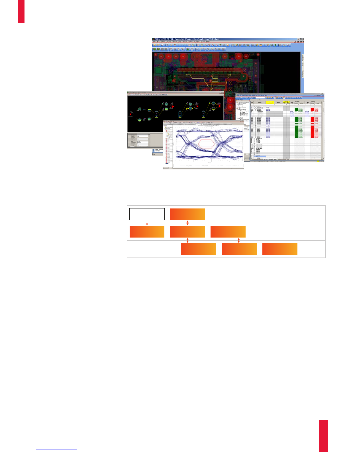
Figure 1: No translation is required to analyze selected signals from the physical board or extract them into the
SigXplorer module. Analysis results are reported in the same constraint manager used by Allegro PCB Editor.
Coupled differential pairs and nets extended through discrete components (x-nets) are automatically identified,
analyzed, and/or extracted.
Figure 2: An Allegro PCB SI and PCB PI option allows engineers to explore and develop optimum constraints and
power decoupling strategies within a constraint-driven design flow.
CONSTRAINT-DRIVEN
DESIGN METHODOLOGY
Cadence PCB SI technology works seamlessly with the constraint management
system of the Allegro PCB Design Suite.
Constraints derived through simulation
can be put into an Electrical Constraint Set
(EC Set) from within the topology canvass,
SigXplorer. These EC Sets can then be
applied to other nets in the design through
the constraint management system found
in Allegro PCB SI, Allegro Design Entry
HDL, and Allegro PCB Design. Designers
can use the constraints developed through
simulation and exploration and enable a
front- to back-end constraint-driven
design process. (See Figure 2.)
POWER INTEGRITY
Allegro PCB SI features both DC and AC
power integrity capabilities. Allegro PCB
SI includes static IR drop (DC) analysis
technology that verifies that the power
distribution system can provide sufficient
current to drive signals. The analysis
considers effects due to trace neck-down;
Swiss-cheese planes created by components with dense pin grid arrays; and
reduction of available copper caused by
trace routing on power and ground
planes. The analysis also takes into
account all vias that connect multiple
ground planes of the same net. Results
can be viewed in a graphical voltage drop
www.cadence.com
CADENCE PCB SIGNAL AND POWER INTEGRITY
2
Page 3

display (See Figure 3.) or in a report that
Without
CDR
With
CDR
shows voltage drop at any pin that is
marked as a current sink. Users can also
view relative and absolute voltage drop
at any point on the net.
AC power integrity is accomplished with
Allegro PCB PI, an option to Allegro PCB
SI. Its unique, integrated design and analysis environment takes the guesswork out
of quantifying and controlling noise in
power delivery systems. Engineers can
focus on the design instead of struggling
with data translation issues between the
CAD system and the analysis engines.
Allegro PCB PI integrates proven technology from Sun Microsystems into the
Cadence design and analysis environment
to address the power delivery issues
encountered in high-speed design.
Frequency domain simulation allows users
to quantify the impedance of the power
delivery system across the frequency
range of interest. In addition, the effectiveness of the decoupling capacitor selection and placement can be verified in the
time domain, where ripples in the voltages can be measured and optimized.
Figure 3: Static IR drop can be performed within the same user interface as signal integrity analysis. Engineers can
verify power delivery and signal quality from a single environment.
Chip current profiles accurately characterize a target impedance in Allegro PCB PI.
In addition, capacitance on the chip and
inductance from the package, or package
and die power delivery models, can be
assigned to an arbitrary position on a
two-dimensional plane structure on the
board to perform frequency or time
domain simulations.
SERIAL LINK DESIGN
METHODOLOGY
When engineers face today’s demands for
faster data throughput, each section of
the interface takes on greater complexity.
Transceivers feature dynamic equalization
and clock and data recovery algorithms
that require advanced modeling techniques. S-parameters for IC package
models must be used to accurately characterize interconnect from the die to the
package pin. And PCB structures must be
carefully characterized such that signal
loss, frequency-dependent materials, and
impedance discontinuities are all accurately represented through broadband
s-parameter interconnect models.
Figure 4: Multi-gigabit serial links can be confirmed to be electrically compliant with interface standards such
as PCI Express 2.0 through the use of eye masks, algorithmic transceiver models (IBIS-AMI), and high-capacity
(million-bit) simulation.
The Allegro PCB SI solution features
integrated field solvers (including 2D
full-wave FEM), support for the IBIS 5.0
algorithmic model interface (AMI) standard for describing SerDes signal processing, and accurate analytical via modeling
(narrowband, wideband, s-parameter).
Allegro PCB SI is a uniquely integrated
and accurate solution for serial link design
and compliance testing. It combines the
ability to accurately model from die to die,
while providing high-capacity (millions of
bits) simulation and statistical analysis
techniques that ensure electrical compliance of industry-standard protocols such
as PCI Express and Serial ATA.
Eye diagrams with compliance eye masks
along with bathtub curves are among the
waveviewer options that engineers have
to measure for interface compliance. (See
Figure 4.) Using Allegro PCB SI, engineers
www.cadence.com
CADENCE PCB SIGNAL AND POWER INTEGRITY
3
Page 4

Mentor Board Station flow. A
bidirectional interface with the Mentor
Board Station enables analysis and routing
within Allegro PCB SI, with the final
results committed back to the Mentor
Board Station environment so that
existing manufacturing output processes
are preserved.
OPERATING SYSTEM
SUPPORT
Allegro platform technology:
• SunSolaris
• Linux
Figure 5: Engineers can validate timing requirements on routed source synchronous signals (e.g., DDR3) through
a methodology that prevents unnecessary simulations. Efficient post-route bus analysis helps ensure that critical
project deadlines are met.
can perform serial link analysis more
thoroughly and more efficiently than with
proprietary tools supplied by semiconductor and SerDes vendors.
SOURCE SYNCHRONOUS
BUS ANALYSIS
METHODOLOGY
Allegro PCB SI provides a quick and easy
methodology to perform post-layout
analysis of all the signals associated with
a source synchronous bus. It shortens the
time to simulate various configurations
(read/write, active, idle) associated with
the functioning of source synchronous
buses with or without on-die termination
(ODT). The Allegro PCB SI solution allows
signals to be associated and to save such
associations with the design database.
Users have a choice of performing reflection analysis or a more comprehensive
analysis with crosstalk included. Allegro
PCB SI enables engineers to derate setup
and hold margins through user-defined
derating tables for different signals in the
source synchronous bus. (See Figure 5.)
ADDITIONAL FEATURES
Estimated crosstalk. This feature allows
users to reduce the number of required
layers by creating crosstalk tables that
drive interactive and automatic routing
to maintain crosstalk budgets.
Design link (package-board or multiboard). Interconnects from multiple PCB
and IC package designs can be combined
using Allegro PCB SI design link technology to analyze die to die through packages, boards, and connectors.
EMI analysis and rule checking. Single-
or coupled-net EMI simulation along with
a comprehensive rule-checking engine,
EMControl, enables engineers to design
for EM compliance.
Model integrity. Users can create,
manipulate, and validate models quickly
in an easy-to-use editing environment.
Support is available for IBIS, Spectre,
Mentor/Quad XTK, and Synopsys HSPICE
(requires HSPICE simulator and license,
which is not included with Allegro PCB SI).
PCB Design Planner option. Engineers
can evaluate placement strategies with
this floorplanning option—used in conjunction with design logic authoring
tools—and assign design intent by
embedding constraints in the front-end
design database.
Resource Library. A comprehensive
library of technical papers, design-in IP
(for example, PCI Express and DDR2), and
how-to movies are available by visiting
cadence.com (Products & Solutions >
PCB Design > Resource Library).
• IBMAIX
• Windows
OrCAD technology:
• Windows
CADENCE SERVICES
AND SUPPORT
• Cadenceapplicationengineerscan
answer your technical questions by
telephone, email, or Internet; they can
also provide technical assistance and
custom training.
• Cadencecertiedinstructorsteachmore
than 70 courses and bring their realworld experience into the classroom.
• Morethan25InternetLearningSeries
(iLS) online courses allow you the flexibility of training at your own computer
via the Internet.
• SourceLink
gives you answers to your technical
questions—24 hours a day, 7 days a
week—including the latest in quarterly
software rollups, product change release
information, technical documentation,
solutions, software updates, and more.
®
online customer support
www.cadence.com
CADENCE PCB SIGNAL AND POWER INTEGRITY
4
Page 5

MAJOR FEATURE SUMMARY FOR ALLEGRO PCB SI PRODUCTS
OrCAD Signal
Explorer
PCB SI product comparison grid (OrCAD, Allegro L/XL/GXL)
Macro modeling support (DML) • • • •
IBIS 4.2 support • • • •
IBIS ICM model support • • • •
Spectre-to-DML • • • •
HSPICE-to-IBIS • • • •
Graphical topology editor • • • •
Lossy transmission lines • • • •
Coupled (3 net) simulation • • • •
Differential pair exploration and simulation • • • •
Custom stimulus • • •
Topology append • • •
Generate estimated crosstalk tables • • •
Detailed simulation reports • • •
Coupled (>3nets) simulation • • •
Allegro Physical Viewer Plus • • •
Differential pair extraction from Allegro PCB Editor • • •
Differential pair extraction from Allegro Design Entry HDL • • •
Current probes
Multi-terminal black boxes in topologies • • •
Custom measurement • • •
Post-layout selection and crosstalk simulation from Allegro PCB Editor • • •
HSPICE interface
Differential signal constraint capture SI Performance • •
Comprehensive simulation SI Performance • •
Sweep simulations SI Performance • •
Constraint development and capture of topologies SI Performance • •
Wide band analytical via model generator SI Performance • •
Topology apply Design Planner • •
Constraint-driven floorplanning and placement Design Planner • •
Allegro Constraint Manager Design Planner • •
Color-coded real-time feedback on violations Design Planner • •
Spectre transistor-level model support • •
Source synchronous bus analysis • •
Batch simulation • •
EM Control: rules development • •
EM Control: rules checking • •
EMI differential simulation • •
Constraint-driven routing • •
Allegro PCB Router XL • •
Static IR drop analysis • •
Simultaneous switching noise (SSN) analysis • •
S-Parameter DC extrapolation S-Parameters S-Parameters •
S-Parameter generation from stack-up S-Parameters S-Parameters •
S-Parameter plotting in SigWave S-Parameters S-Parameters •
Time domain simulation of S-Parameters S-Parameters S-Parameters •
Library management of S-Parameters in model integrity S-Parameters S-Parameters •
Allegro PCB SI L Allegro PCB SI XL Allegro PCB SI GXL
• • •
SI Performance • •
www.cadence.com
CADENCE PCB SIGNAL AND POWER INTEGRITY
5
Page 6

MAJOR FEATURE SUMMARY FOR ALLEGRO PCB SI PRODUCTS
OrCAD Signal
Explorer
PCB SI product comparison grid (OrCAD, Allegro L/XL/GXL)
Coupled via model generator for pre-layout explorations S-Parameters S-Parameters •
High-capacity channel simulation Serial Link Serial Link •
Optimum pre-emphasis bit configurations (“tap settings”) Serial Link Serial Link •
BER prediction Serial Link Serial Link •
Bathtub curves Serial Link Serial Link •
Channel compliance—statistical analysis Serial Link Serial Link •
Post-layout MGH extraction •
Voltage ripples in time domain
Impedance requirements calculator PI Option PI Option PI Option
Decoupling capacitor selection and placement PI Option PI Option PI Option
VRM editor
Decoupling capacitor library editor PI Option PI Option PI Option
Cross-probing between waveform and design canvas PI Option PI Option PI Option
Frequency domain analysis PI Option PI Option PI Option
IC switching currents
Package and die parasitics PI Option PI Option PI Option
Notes:
SI Performance: Allegro PCB SI
Performance Option
Allegro PCB SI L
PI Option PI Option PI Option
PI Option PI Option PI Option
PI Option PI Option PI Option
Allegro PCB SI XL Allegro PCB SI GXL
S-Parameters: Allegro PCB SI
S-Parameters Option
Serial Link: Allegro PCB SI Serial Link Option
PI Option: Allegro PCB PI Option
Design Planner: Allegro PCB Design
Planner Option
For additional information,
contact Cadence sales at:
+1.408.943.1234
or log on to:
www.cadence.com/
contact_us
© 2008 Cadenc e Design Syst ems, Inc. All rights reser ved. Cadence, Allegro, OrC AD, and Sourc eLink are reg istered trade marks and the Cadence logo is a
trademark of Cadence Design Systems, Inc. All others are properties of their respective holders.
20808/7430 11/08 MK/MVC/CS/PDF
 Loading...