

Page 1

DATASHEET
A
p
p
l
i
c
a
b
i
l
i
t
y
C
o
n
s
u
l
t
i
n
g
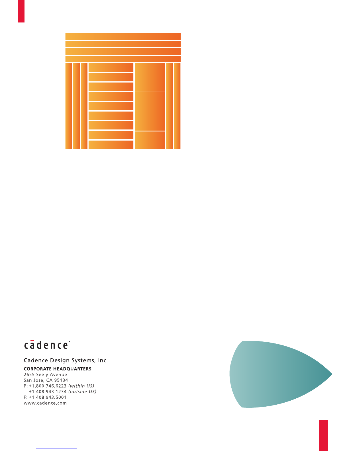
Low-Power Techniques
Multiple voltage thresholds, low-power clocking
multiple supply voltages, power shut-off
Design Environment
Infrastructure, process selection,
library qualification
Management
Planning, metrics, ECO
Design
Creation
Architecture, RTL, CPF,
synthesis, DFT
Verification
Functional,
implementation
power-grid sign-off
Physical
Implementation
Prototyping, parasitics,
floorplanning, timing
and SI closure
M
e
t
h
o
d
o
l
o
g
y
I
n
f
r
a
s
t
r
u
c
t
u
r
e
Segment
Representative
Design
I
P
CADENCE LOW-POWER
METHODOLOGY KIT
Meeting the power consumption and density requirements of
modern electronic devices means engineers must consider
power at all stages of the design process—from architecture
through implementation. If not done properly, however, adding
advanced power management to an already complex design
process significantly increases project costs and risks. The
Cadence Low-Power Methodology Kit enables design and
implementation teams to streamline the adoption of low-power
techniques, optimize their usage, and get predictable results
INTRODUCTION
Ever-increasing device integration, as
well as the need for advanced mobile
applications, is driving the need to reduce
power consumption across a wide range of
design types (wireless, networking, and
consumer). Reducing power usage not only
helps improve battery life in mobile devices
but also improves manufacturability at
smaller device geometries, and reduces
overall system and packaging costs.
Using traditional design techniques to target
low-power designs leads to a complex,
manual, unpredictable and highly error-prone
flow. Achieving meaningful power reductions
requires more than this “bolt on” approach of
adding new capabilities into existing flows.
Meaningful power reduction is only achieved
by taking a holistic approach to low-power
design from architectural choices all the way
through final physical implementation and
signoff. Verification throughout all stages is
critical since advanced power management
techniques have significant functional impact
on the design.
with minimal risk.
CADENCE LOW-POWER
METHODOLOGY KIT
The Cadence Low-Power Methodology Kit
provides users with a complete front to
back methodology for low-power
implementation and verification. It
combines industry-leading Cadence lowpower technology from the Incisive and
Encounter platforms, with a single power
specification format (CPF) and proven
methodologies.
The kit is more than just methodology. It
captures best practices in the form of
executable flows, as well as detailed
checklists that ensure a high level of
automation and a clean handoff between
different tasks and groups within the
design team. The kit is highly modularized
Page 2
• Detailed low-power methodology
Multiple Threshold Voltage
Low Power Clocking
Multiple Supply Voltages (MSV)
Power Shut Off (PSO)
Library Qualification
Process Selection
Library Qualification
Process Selection
Infrastructure
Architecture Trade-off Low Power
Functional
Verification
Low Power
Implementation
Verification
Power Grid
Sign-off
RTL Design
CPF Creation
Low Power Synthesis
Power Aware DFT
Power Planning
Low Power Floorplanning
Timing and SI Closure
Prototyping and Parasitics
Correlation
guide, covering all aspects of lowpower implementation
• Reference flow implementations with
step-by-step walkthroughs
• Detailed documentation of the SRD and
reference flow
• Detailed flow checklists, and trade-off
analysis
• Expert consulting designed to map the
verified and demonstrated methodologies
to a specific customer design
The Low-Power Methodology Kit utilizes
and integrates with the following
technologies (not included)
to allow for incremental adoption and to
allow teams to focus on what is most
critical for the design.
All flows are demonstrated on the
Segment Representative Design (SRD)—a
real world 802.11 based design—that
integrates multiple IP blocks from ARM,
ChipIdea, Wipro, TSMC and Virage.
The kit also includes expert applicability
consulting to ensure teams can realize
immediate benefits by adapting the kit
contents to their own design and design
environment.
BENEFITS
• Enables teams with limited experience
in implementing advanced low-power
techniques to adopt them in their
design with significantly reduced risk
• Provides significant productivity
improvements through supplied
infrastucture
• Restores schedule predictability through
application of proven processes
• Avoids common problems in low-power
design through expert knowledge and
best practices
• Optimizes flows and tradeoff analysis to
ensure technology is applied to give the best
results and improve overall quality of silicon
• Reduces overall packaging and system
cost by allowing for expanded
application of low-power techniques
KIT COMPOSITION AND
INTEGRATION
The Cadence Low-Power Methodology Kit
includes the following;
• Wireless segment representative design
(SRD), including all required views for
RTL design, physical implementation,
and verification (including testbench)
• Cadence Logic Design Team Solution
• Incisive Plan-To-Closure Methodology
• Incisive Enterprise Family
• Incisive Formal Verifier
• Encounter RTL Compiler
• Encounter Test
• First Encounter
• SoC Encounter
• Encounter Conformal EC
• Encounter Conformal LP
• Voltage Storm
© 2007 Cadence Design Systems, Inc. All rights reserved. Cadence is a registere d tradema rk
and the Cadence logo is a trademark of Cadence Design Systems, Inc.
7477 0507 KM/MVC/JA/PDF
For more information
contact Cadence sales at:
+1.408.943.1234
or log on to:
www.cadence.com/
contact_us
 Loading...