

Page 1

DATASHEET
CADENCE LITHO
PHYSICAL ANALYZER
Full-Chip, Model-Based Design Manufacturability Checking
and Contour Shape Prediction
A comprehensive model-based design manufacturability
checker, Cadence® Litho Physical Analyzer detects
manufacturability issues missed by traditional DRC check
in a fraction of the time required by solutions based
on OPC and lithography simulation. Silicon-proven and
foundry-endorsed, it quickly and accurately accounts for
systematic manufacturing variations on all critical layers,
helping designers improve yield during physical design
implementation.
CADENCE LITHO
PHYSICAL ANALYZER
At 65 nanometers and below, lithography,
etch, and mask systematic manufacturing
variations surpass random variations as
the prime limiters to catastrophic and
parametric yield loss. The interaction
of manufacturing shapes within the
optical proximity halo and the spatially
partially-coherent lithography projection
systems creates highly non-linear
systematic variations at different process
conditions that cannot be captured
by rules or pattern matching. These
systematic shape variations, dependent
on specific layout shape context, result
in predictable catastrophic errors such
as necking (opens) and bridging (shorts).
Furthermore, the litho-induced systematic
shape variations of interconnect and gate
have a non-linear impact on electrical
parameters such as timing, leakage
power, and signal integrity.
Figure 1: Cadence Litho Physical Analyzer use model
Page 2
Cadence Litho Physical Analyzer helps
designers solve these systematic designfor-manufacturing (DFM) challenges.
It is a full-chip, model-based design
manufacturability checker that designers
can use to detect lithography hotspots
based on fast and accurate silicon contour
prediction across the process window. It
creates fixing guidelines to help designers
or design tools correct these hotspots.
These predicted silicon contours can be
used for further electrical DFM analysis
with Cadence Litho Electrical Analyzer,
enabling designers to improve parametric
yield and chip performance by accurately
determining the impact of systematic
manufacturing variations during design.
BENEFITS
• Detects yield-limiting variability
hotspots based on foundry-certified
technology files
• Helps designers improve printability and
yield with fixing guidelines
• Checks cells in seconds / full chips in
hours with proprietary formulation that
allows fast and accurate silicon contour
prediction across the process window
• Integrates with most commonly used
design flows
• Offers fast runtimes and a
designer-friendly use model
• Compatible with existing design farms
for easy adoption by design teams
• Integrates with Cadence Litho
Electrical Analyzer
FEATURES
MODEL-BASED MANUFACTURING
SHAPE PREDICTION
Traditional approaches to deal with
manufacturing variations are no longer
adequate. Design rule checking (DRC)
alone does not prevent catastrophic yield
loss due to systematic shape variations;
additionally, DRC rules to address growing
DFM issues become prohibitive in number
and complexity. Post-GDSII OPC uncovers
printability problems that frequently
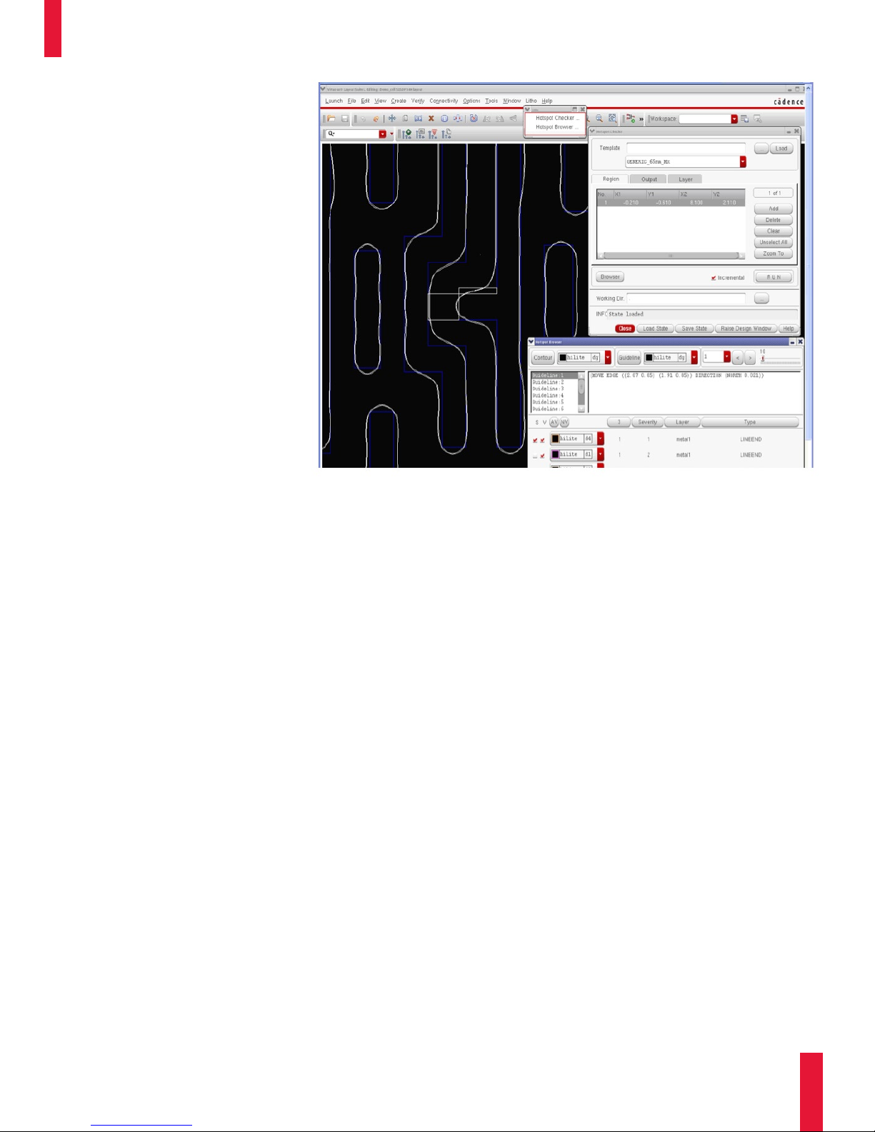
Figure 2: Litho Physical Analyzer hotspot browser Layout Editor
require actual design changes when there
is limited freedom after tapeout, making
design closure unpredictable. Running
post-GDSII OPC tools during layout is not
feasible, because it takes days for every
layer to run a typical design through OPC.
Designers can restrict their design style
in an attempt to improve yield, but
this method limits the use of leadingedge processes that optimize area
and performance. Only model-based
predictive approaches (that are not based
on moving post-GDSII OPC tools to the
designer’s desk) are fast enough to let
designers uncover hotspots during design
implementation and make real-time
design adjustments to eliminate them.
Cadence Litho Physical Analyzer is a
full-chip, model-based design manufacturability checker—silicon-proven and
endorsed by all major foundry platforms—
that designers can use to find and fix
hotspots and predict contours across
process conditions. It uses a patentpending, model-based, non-linear optical
transformation algorithm that allows
designers to quickly and accurately detect
potential manufacturing failures during
physical design that would otherwise be
found after tapeout in mask or silicon.
The compact models encapsulate all
necessary RET, OPC, mask, etch, and
lithography effects on both device and
interconnect, and predict accurate
contours for the entire chip from drawn
layout in a matter of hours. Cadence
Litho Physical Analyzer is typically an
order of magnitude faster than other
model-based tools.
SOPHISTICATED HOTSPOT
DETECTION AND CORRECTION
GUIDELINES
Litho Physical Analyzer identifies hotspots
based on fab-designated criteria or litho
yield sensitivity (LYS) metrics. It sorts
hotpots by type and criticality, and prechecked blocks can be excluded by name,
area, or marker layer. The non-linear
optical transformation algorithm also
allows generation of automatic fixing
guidelines that are input into the user’s
choice of physical design tools, such as
Cadence Virtuoso® Layout Suite and
www.c a den c e.c om
CAD EN CE L ITH O PHYS ICA L ANALY ZE R
2
Page 3

Cadence Chip Optimizer. Litho Physical
Analyzer integrates with current library,
IP, custom analog, and cell-based digital
physical design flows.
DESIGNER FRIENDLY
With a usage model similar to DRC, Litho
Physical Analyzer works from layout and
fab technology file input to produce a fullchip report that flags DFM hotspots such
as opens and shorts, contact coverage,
gate variability, and line-end pullback in the
original layout. It also provides engineering
change order (ECO) guidelines. Litho
Physical Analyzer guides designers to make
changes only when there is a problem
due to process-design interaction. The
results and recommendations can be easily
exported to most layout editors and/or
place-and-route tools.
Litho Physical Analyzer provides an
interface to Virtuoso Layout Editor,
enabling designers to browse hotspots
and guidelines and perform incremental
check directly from the layout window.
For cell-based designers, Cadence Chip
Optimizer uses Litho Physical Analyzer’s
hotspot and guideline results to automatically correct hotspots while maintaining
timing and DRC.
COMPREHENSIVE
FOUNDRY SUPPORT
Litho Physical Analyzer’s unique
formulation, which makes it accurate
and OPC-tool independent, eases and
speeds its adoption by all major foundry
platforms and IDMs. Litho Physical
Analyzer is used by major foundries
and their customers to systematically
detect hotspots on designs prior
to manufacturing.
Figure 3: Litho Physical hotspot browser in Cadence Chip Optimizer
SPECIFICATIONS
FOUNDRY SUPPORT
• Certified and supported by leading
foundries and IDMs
• Flow-tested and qualified with foundry
DFM data kits (DDKs)
FORMAT SUPPORT
• Design input: GDSII, LEF/DEF
• Design output: GDS, HIF, DLD (contour
database for Cadence Litho Electrical
Analyzer)
PLATFORMS
• Linux (32-bit, 64-bit)
CADENCE SERVICES
AND SUPPORT
• Cadence application engineers can
answer your technical questions by
telephone, email, or Internet—they can
also provide technical assistance and
custom training
• Cadence certified instructors teach
more than 70 courses and bring their
real-world experience into
the classroom
• More than 25 Internet Learning
Series (iLS) online courses allow you
the flexibility of training at your own
computer via the Internet
• SourceLink® online customer support
gives you answers to your technical
questions—24 hours a day, 7 days
a week—including the latest in
quarterly software rollups, product
change release information, technical
documentation, solutions, software
updates, and more
www.c a den c e.c om
CAD EN CE L ITH O PHYS ICA L ANALY ZE R
3
Page 4

© 2008 Cadence Design Systems, Inc. All rights reserved. Cadence and V irtuoso a re regist ered trad emarks an d the Cad ence logo is a trademark of Cadence
Design Systems, Inc. All others are properties of their respective hol ders.
20410 04/08 MK/FLD/CS/PDF
For more information,
Email us at
info@cadence.com
or visit
www.cadence.com
 Loading...